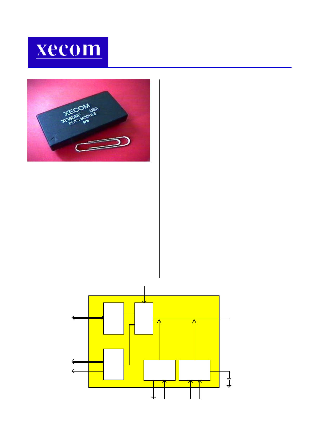
XECOM XEISDNP Datasheet

XEISDNP
Single Module ISDN Analog Telephone
(POTS) Equipment Interface
Description
The XEISDNP is a multichip module designed
to interconnect analog telephone equipment such
as a handset, a Group 3 Fax machine, or an
analog modem to an ISDN Terminal Adapter. The
device provides all the functions needed to
support conventional analog subscriber equipment including voice/fax data CODEC, DTMF
tone detector, RING signal generator and telephone line power feed. It provides a simple,
compact solution for designers who wish to integrate an ISDN digital interface into their designs
but also protect their user’s investment in their
existing POTS (Plain Old Telephone Service)
equipment.
The XEISDNP is designed to interface with the
XECOM XEISDNU Single Module ISDN Terminal
Adapter.
Features
• Small size: 2.75" x 1.38" x 0.42"
• Adds POTS function to XECOM XEISDNU
• Supports standard analog telephones, Group 3
FAX machines, and analog modems
• Provides all Central Office functions to analog
telephone equipment
• Uses GCI (IOM-2) or IDL standard communication bus to exchange voice/fax/data between
its on board CODEC and ISDN Terminal
Adapter
• Pin configurable to Mu-law or A-law PCM
coding
• Programmable for B1 or B2 channel of the
ISDN Basic Rate interface
• Uses standard data bus to access DTMF
codes from the ISDN TA
• Built-in 150V DC inverter to support RING
signal generation
• Built in power supply provides the telephone
handset with 30 to 50 mA current
RING GeneratorDC Power supply
10uF/250V
+
To telephone set
or FAX machine
CODEC
Voice/FAX
for
Data
DTMF
Decoder
GCI or IDL Bus
Three state
DTMF ready
DTMF output
Off Hook Power CTRL RING CTRL
Voice/FAX/Modem signal path (Analog)
ROUTE
SWITCH
Route CTRL

Page 2 XEISDNP
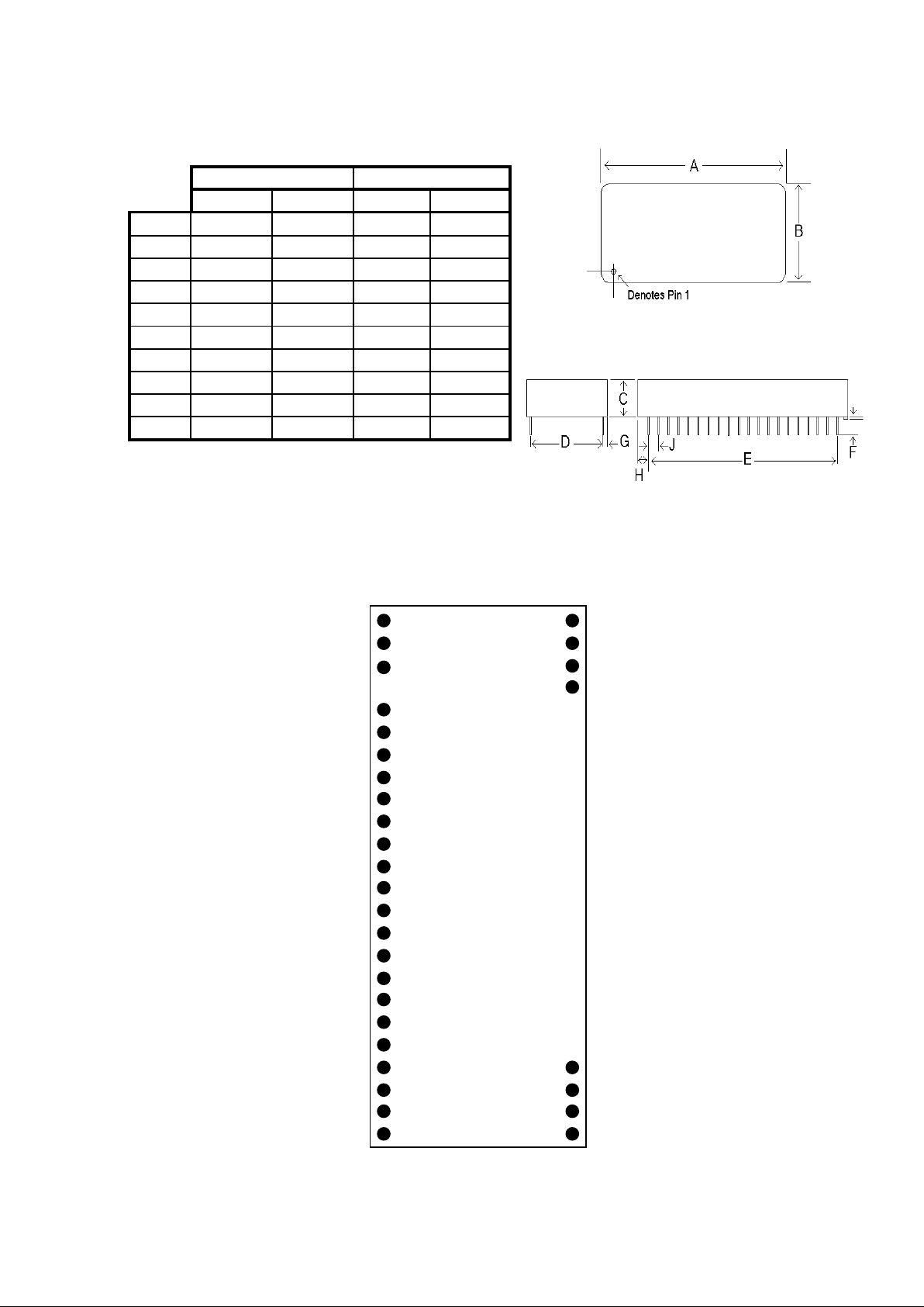
Mechanical Specifications
INCHES METRIC (MM)
MIN MAX MIN MAX
A
2.740 2.760 69.60 70.10
B
1.370 1.390 34.80 35.31
C
0.420 0.430 10.67 10.92
D
1.190 1.210 30.23 30.73
E
2.290 2.310 58.17 58.67
F
0.125 0.200 3.18 5.08
G
0.080 0.100 2.03 2.54
H
0.215 0.235 5.46 5.97
I
0.090 0.110 2.29 2.79
J
0.020 0.025 0.51 0.64
(Total pin count is 24 per side view.)
Pin Configuration
(Blank pin location indicates no pin installed)
TTIP
RING
DC_OUT
NC
DR/RXDIN
DT/TXD1
FST/CD1N
FSR/TXD3
NC
NC
OH
DTMF_RDY
RING_EN
RING_DC
PWR_CTRL
ROUTE_CT
/PDI/DREQ
D4
D5
D6
D7
-12V
GND
++5V
GND
B_M_CLK/RCLK
GND
GND
Mu/A
NC
+12V
1
2
3
4
5
6
7
8
9
10
11
12
13
14
15
16
17
18
19
20
21
22
23
24
48
47
46
45
44
43
42
41
40
39
38
37
36
35
34
33
32
31
30
29
28
27
26
25

XEISDNP Page 3
Pin Descriptions
Name Pin # Direction Description
TIP 1 I/O Connect to POTS equipment
RING 2 I/O Connect to POTS equipment
DC_OUT 3 Output Test pin for the 150V DC supply for RING signal. Bypass to GND
with 10uF/250V capacitor.
NP 4, 29-44 No pin installed
NC 5,10,11,26 No connection allowed
DR/RXDIN 6 Input Data Receive for IDL or GCI
DT/TXD1 7 Output Data Transmit for IDL or GCI
FST/CDIN 8 Input Frame Synchronize Transmission: This pin accepts an 8KHz
clock that synchronizes the output of the serial PCM data at the
DT pin.
FSR/TXD3
(B2/B1)
9 Input When an ISDN mode (IDL or GCI) has been selected with
BCLKR, this pin selects either B1 (logic 0) or B2 (logic 1) as the
active data channel.
NC 10,11 No connection allowed
OH 12 Output On/Off hook status of POTS equipment
DTMF_RDY 13 Output Signal to inform controller a DTMF tone has been detected
RING_EN 14 Input Control to cycle on and off theRING voltage when DC_EN is
active.
DC_EN 15 Input Control signal to enable 150 VDC generation for RING signal.
This pin should be held high from before the first RING ENable
until the phone set goes off hook or the caller hangs up.
PWR_CTRL 16 Input Control signal for powering up POTS telephone set.
ROUTE_CTRL 17 Input Control pin for voice signal switching inside the module.
/PDI 18 Input Power down mode control.
D4 - D7 19-22 Output Connect to controller main data bus low byte, lines D4 - D7;
carries DTMF code.
-12V 23 -12V DC power supply
GND 24,28,45,47 Ground
+12V 25 +12V DC power supply
Mu/A 27 Input Connect to logic 1 (+5V) selects A law and logic 0 (GND) selects
Mu law
B_M_CLK
/RCLK
(IDL/GCI)
46 When this pin is held at a logic 1, FST, BCLKT, DT and DR
become IDL mode. When this pin is held at a logic 0, FST,
BCLKT, DT and DR become GCI mode.
VCC 48 +5V DC power supply
 Loading...