XECOM XE9601 Datasheet

Xecom, Inc. XE9601
9600 BPS Data Modem Module
XE9601
08-97
Description
Xecom's XE9601 provides high-speed data
transfer in a compact component. The XE9601
is a complete modem not just a modem chip. It
includes the telephone interface and all required
RAM and ROM. The XE9601's internal
telephone interface permits Xecom to offer user
transferable FCC Part 68 registration on the
XE9601. The XE9601 connects to the host
through a TTL level serial interface and to the
telephone network through a user-supplied RJ11
jack.
Xecom's XE9601, XE1401, XE3301 and
XE2401 share a common pin configuration.
This permits Xecom customers to select the
appropriate data rate from 2400 to 33,600 bps.
Features
• Small Size; 2.75 " x 1.38" x 0.55"
• Modem Protocols: CCITT V.32, V.22bis,
V.22, V.21; Bell 212A and 103
• Pin compatible with Xecom's XE2401
• User Transferrable FCC Part 68
Registration
• Modem control with "AT" commands
• Modem link speed to 9600 bps
• Low power, single +5V supply
Operating Power 1.0 W (Typ.)
Idle Power 125 mW (Typ.)
Sleep mode: 50 mW (Typ.)
xecom
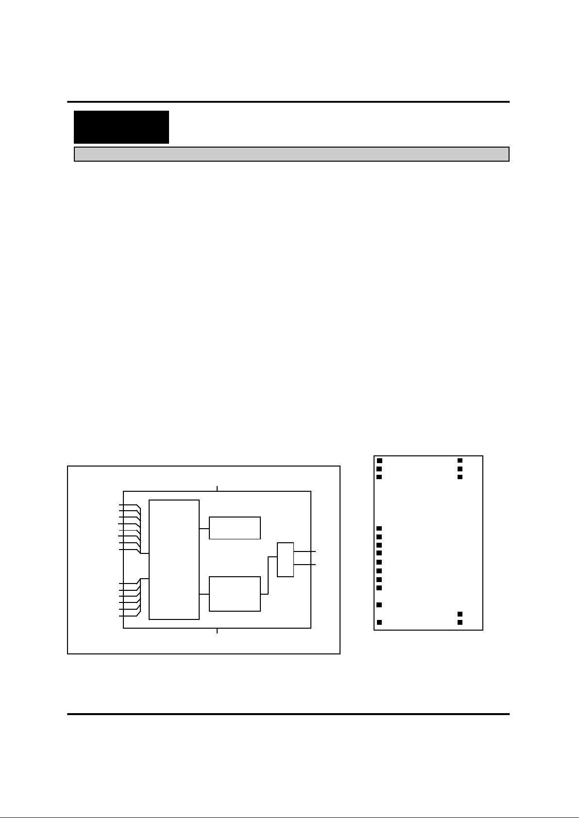
PIN CONFIGURATION
RESET
N/C
RXD
/DTR
/AA
/CTS
OH
TXD
/RTS
NC
/RI
TIP
RING
AUX
I/O
ANALOG
FRONT END
DAA
TIP
RING
V
cc
GND
CONTROLLER
MEMORY
/RTS
/DTR
/CTS
/DSR
TXD
RXD
/DCD
/RI
RESET
OH
AR
AMP
/HS
/AA
RS232
I/O
VCC
/DSR
/DCD
AMP
GND
Block Diagram
1
2
3
9
10
11
12
13
14
15
16
18
20
40
39
38
22
21

Xecom, Inc. (2) XE9601
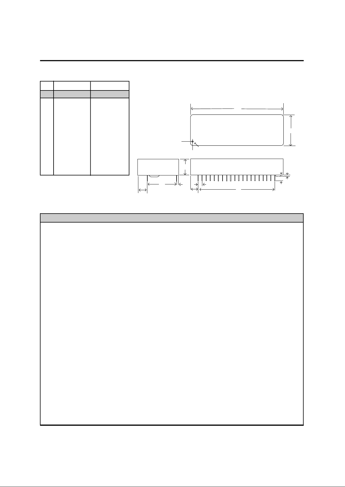
Mechanical Specifications - XE9601
A
B
Denotes Pin 1
C
D
G
J
H
E
F
K
L
A 2.74 2.760 69.60 70.10
B 1.370 1.390 34.80 35.31
C 0.490 0.510 12.45 12.95
D 0.890 0.910 22.61 23.11
E 1.890 1.910 48.01 48.51
F 0.175 0.250 4.41 6.35
G 0.080 0.100 2.03 2.54
H 0.415 0.435 10.54 11.05
J 0.090 0.110 2.29 2.79
K 0.020 0.040 0.51 1.02
L 0.380 0.400 9.65 10.16
Pins = 0.025 inch square pin
All pins tin-plated
INCHES METRIC(MM)
PIN MIN MAX MIN MAX
1 RESET I Hardware reset pin, Input, active High, TTL. A high on Pin 1 initiates a hardware reset.
An external reset is not required or recommended. The Reset pulse must be a minimum
of 200 milliseconds long.
2 N/C No Connection
3 RXD O Received Data, Output, TTL. Serial data output to the host. A logic "high" represents a
"mark" and a logic "low" represents a "space".
9 \DTR I Data Terminal Ready, Input, active Low, TTL. "&D" sets the function of DTR. The
default, &D2, requires the host to assert DTR to permit a modem link. The modem
drops the call in progress if DTR is revoked and will not connect until DTR is reasserted.
10 \AA O Auto-Answer, Output, active Low, TTL. A low on \AA indicates the modem is configured
to automatically answer an incoming call.
11 \CTS O Clear to Send, Output, active LO, TTL/CMOS. This pin indicates the modem is able to
transfer data.
12 OH O Off-Hook, Output, active High. OH indicates the modem's hookswitch relay is closed.
Hookswitch closure connects the modem to the telephone line.
13 TXD I Transmit Data, Input, TTL. Serial data input from the host. A logic "high" represents a
"mark" and a low represents a"space", TTL.
14 \RTS I Request to Send, input, active LO, TTL. The XE9601 does not use RTS.
15 NC --- No Internal Connection
16 \RI O Ring Indicator, Output, active LO, TTL. When low indicates the modem is receiving a ring
signal.
18 TIP — Tip connection to the phone line(RJ11 pin3) from the internal DAA. The XE9601 is not
sensitive to the battery voltage polarity across Tip and Ring.
20 RING — Ring connection to the phone line(RJ11 pin4) from the internal DAA.
PIN NAME I/O DESCRIPTION
Pin Descriptions

Xecom, Inc. (3) XE9601
21 GND — Ground (0 volts)
22 AMP O Audio output function is set by L & M commands and the value in register S22. This
output can drive a minimum load of 300 ohms.
38 \DCD O Data Carrier Detect, output, active LO, TTL/CMOS. &C sets the DCD function. In the
default condition, AT&C1, DCD indicates the presense of a carrier signal on the
telephone line.
39 \DSR O Data Set Ready, output, active LO, TTL/CMOS. &S sets the DSR function. In the default
condition, AT&S0, DSR is forced true.
40 Vcc — +5 Volts
PIN NAME I/O DESCRIPTION
Pin Descriptions (continued)
Tip
Ring
L1
L2
C1
C2
J1
VCC
Reset
TXD
RXD
+5 Volts
50K
.2 ufd
250 ufd
.05 ufd
10 ohms
8 ohm .5 W
Speaker
AMP
4 3
Line
GND
LM386
/RI
/RTS
/CTS
/DTR
/DSR
/DCD
OH
XE9601
16C450
UART
/DSR
/DCD
SIN
/DTR
/CTS
SOUT
/RTS
/RI
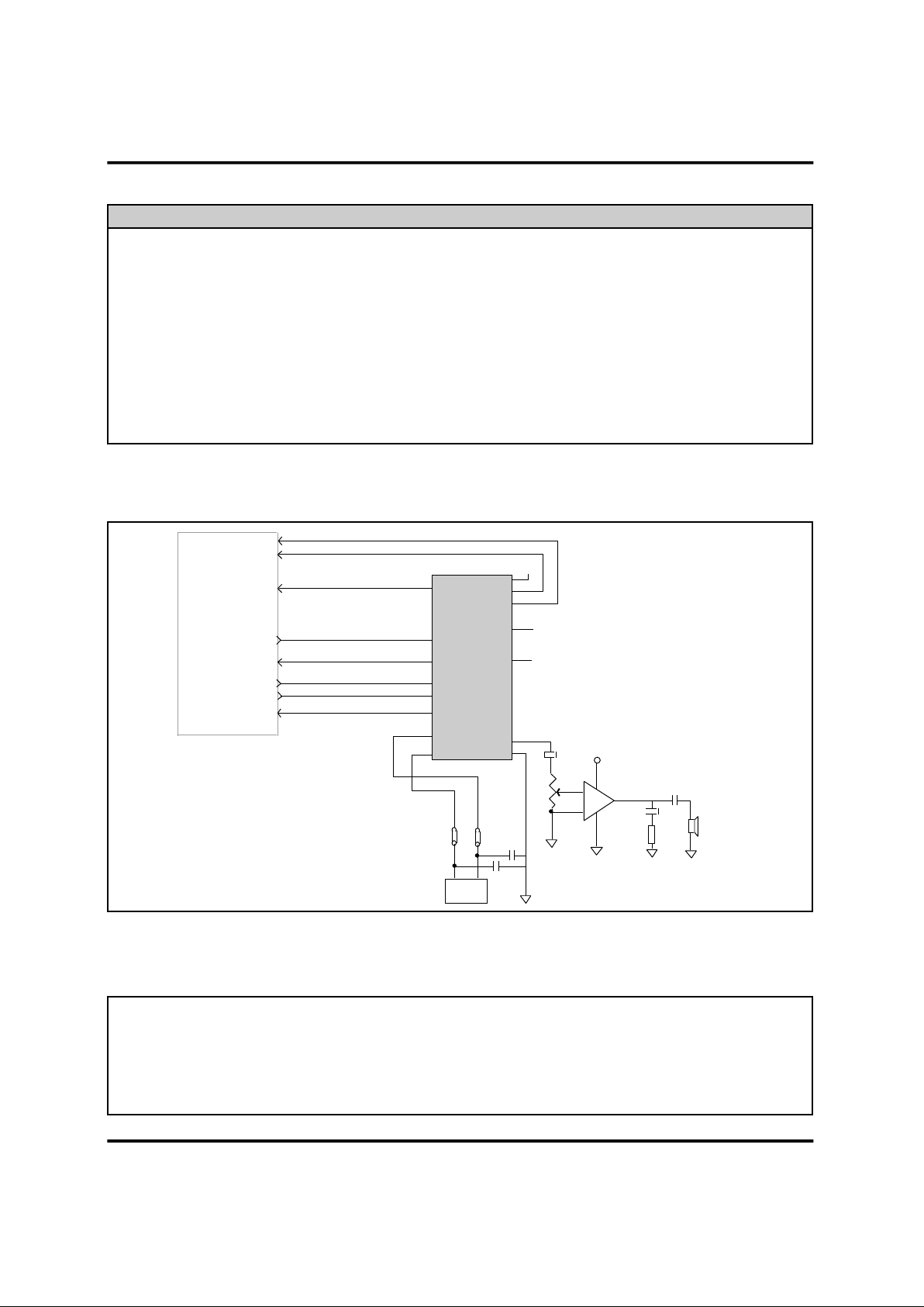
Modem Applications Schematic
Note: RJ11 Pin assignments reference a 6-pin connector. Tip and Ring are the center pins of all RJ11
jacks.
Recommended Parts
Reference Designation Description Recommended Part Number
L1, L2 Ferrite Beads TDK CB30-1812
C1, C2 Capacitors Sprague 30GAT47, 470 pfd, 3000 Volts
J1 RJ11 Jack Stewart SS6446NF
 Loading...