XECOM XE5224FD, XE5224DM Datasheet

Description:
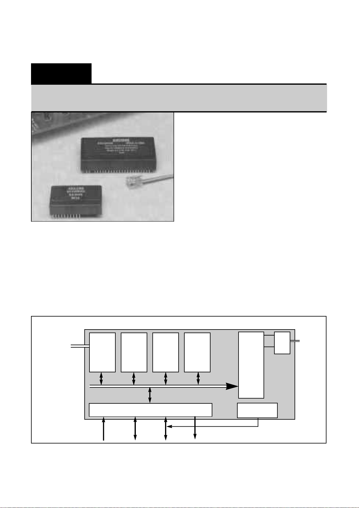
The Blackjack Tele-Controller is a rugged, miniature
controller with an integrated modem. Xecom based the
Tele-Controller on an 80C552 micro-controller. It provides
32 Kbytes each of ROM and RAM, 128 Kbytes of Flash
memory, 26 I/O lines and the modem. The XE5224DM
includes a 2400 bit per second data modem; The XE5224FD
adds send and receive fax . Firmware embedded in the
Tele-Controller provides development tools which allow
manipulation of both program and data memory.
Features:
* Small size: 2.75" x 1.38" x 0.50"
* Philips 80C552 micro-controller, at 14.7456 MHz;
* 26 I/O lines Includes:
Two 8-bit Digital I/O Ports;
Eight I/O lines available as inputs to 10 bit A/D;
Two PWM outputs;
* I/O Compatible with Opto 22/Grayhill series modules;
* 32 Kbyte Pre-programmed internal ROM ;
* 32 Kbyte SRAM for data storage;
* 128 Kbyte Flash memory for program and data storage;
* Real Time Calendar/Clock (External battery backup)
* 2400 bps data modem, XE5224DM or 2400 bps modem
with send & receive fax , XE5224FD;
* Typical Power:
Controller active, Modem idle: +5 Volts @ 55 milliamps;
Controller and Modem active: +5 Volts @ 95 milliamps;
* Serial Port for RS232 or RS485 communications;
* Development Kit available;
* Sturdy, encapsulated construction seals circuits from
harsh environments;
* Industrial Temperature Range available;
XE5224DM & XE5224FD
10-03-95
xecom
Blackjack Tele-Controller
80C552 based controller with 2400 bps data modem (send/receive fax optional)
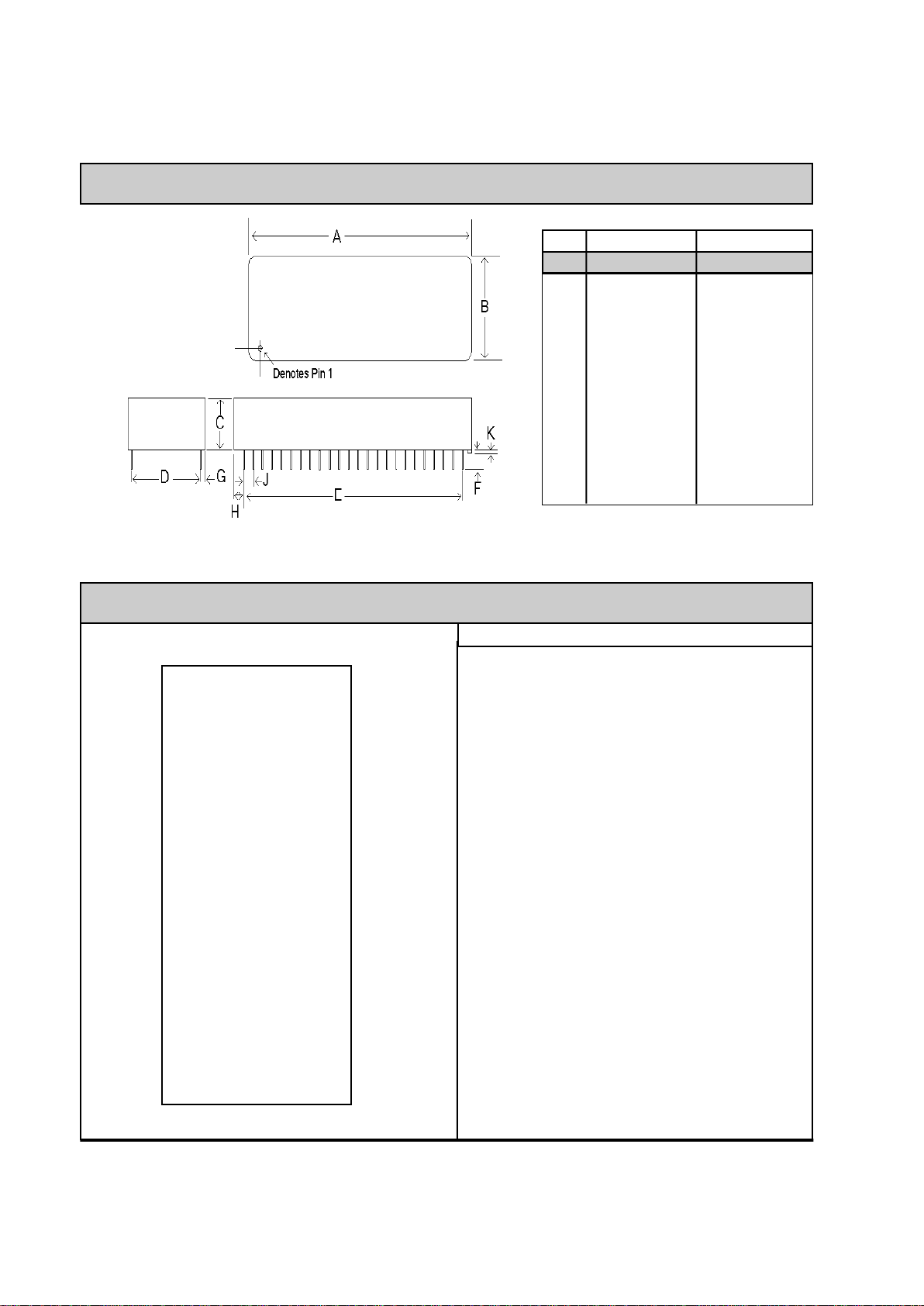
Tele-Controller Block Diagram
Modem
DAA
To
Telephone
Line
80C552
Micro-
controller
32 KByte
SRAM
32 Kbyte
ROM
128 Kbyte
Flash-
Memory
8 Analog/Digital 8 Digital 8 Digital 2 Channels
Input Channels I/O Channels I/O Channels PWM Output
Real-Time
Calendar/Clock
To RS232
or RS485

1 TIP One of the signals forming the two-
wire connection to the telephone line.
The Tele-Controller is not sensitive to
the polarity of the battery voltage on
the telephone line.
2 RING The second wire of the two-wire
connection to the telephone line.
3 N/P No Pin
4 OH Off Hook is an active high output from
the Tele-Controller. A high indicates
the internal modem has seized the
telephone line.
5 SPKR SPKR is the audio output from the
Tele-Controller. It permits the user to
monitor the activity on the telephone
line by connecting a speaker. The
load on SPKR must be at least 300
ohms.
6 /SLEEP SLEEP is an active low output from
the Tele-Controller. A low indicates
the modem within the Tele-Controller
is operating on reduced power in the
"sleep" mode.
7 N/C No connection
XECOM (2) XE5224DM & XE5224FD
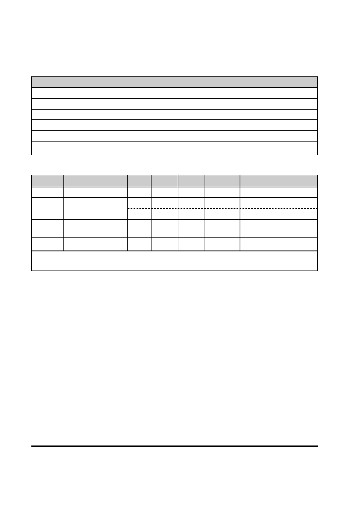
Mechanical Specifications
DIM MIN MAX MIN MAX
A 2.740 2.760 69.60 70.10
B 1.370 1.390 34.80 35.31
C 0.500 0.510 12.70 12.95
D 1.190 1.210 30.23 30.73
E 1.890 1.910 48.01 48.51
F 0.125 0.200 03.18 05.08
G 0.080 0.100 02.03 02.54
H 0.415 0.435 10.54 11.05
J 0.090 0.110 02.29 02.79
K 0.020 0.025 00.51 00.64
INCHES METRIC (MM)
Pin Configuration & Descriptions
1 48
2 Tele-Controller 47
3 46
4 45
5 44
6 43
7 42
8 41
9 40
10 39
11 38
12 37
13 36
14 35
15 34
16 33
17 32
18 31
19 30
20 29
21 28
22 27
23 26
24 25
TIP
RING
N/P
OH
SPKR
/SLEEP
N/C
V.bat
RXD
TXD
RESET
/EW
/INT0
T0
CNFG0
CNFG1
CNFG2
DIO0
DIO1
DIO2
DIO3
DIO4
DIO5
GND
VCC (5V)
DIO15
DIO14
DIO13
DIO12
DIO11
DIO10
DIO9
DIO8
DIO7
DIO6
DA1
DA0
A.VCC
ADI.7
ADI.6
ADI.5
ADI.4
ADI.3
ADI.2
ADI.1
ADI.0
STADC
A. GND
PIN SIGNAL DESCRIPTION

8 V.bat V.bat provides backup power for the
real time clock. Battery voltage must
be at least 3 volts. A "Super Cap,"
NEC FYH0H473Z or equivalent, may
be used in place of a battery.
9 RXD RXD is the serial data input to the
Tele-Controller. A Mark or Logic 1 is a
TTL low; Space is a TTL high.
10 TXD TXD is the serial data output from the
Tele-Controller. A Mark or Logic 1 is
a TTL low; Space is a TTL high.
11 Reset Reset is an active high input to the
Tele-Controller. A high on Reset
initiates a hardware reset . This pin
acts as a Reset ouptut when the TeleController's watchdog timer expires.
12 /EW This active low input enables the
Tele-Controller's watchdog timer and
disables Sleep mode. When not used
this pin must be tied to VCC.
13 /INT0 This active low input acts as an
external interrupt to the TeleController.
14 T0 This active high input provides the
trigger for timer 0.
15 CNFG0 CNFG0 selects Tele-Controller
development or application mode. A
high selects application mode; a low
selects development mode.
16-17CNFG1-2 These inputs select the memory
address configuration of the ROM and
Flash memory. See the charts on
Pages 5 and 6 of this data sheet for
details on how these signals interact.
18-23 DIO0-5 Digital Input/Output Port 1 bits 0-5.
These signals are part of an 8-bit
digital I/O port. If the real-time clock is
to be used, bits 0-2 are needed to
support it. Port 1 alternate functions
include:
bit 0-3 - Capture inputs for timer T2
bit 4 - T2 event input
bit 5 - T2 Timer reset
24 GND GND provides digital ground to the
Tele-Controller.
25 A.GND A.GND provides analog ground for the
Analog inputs to the Tele-Controller.
26 STADC This active high input intiates an
analog to digital conversion. The
analog to digital conversion may also
be started through software.
27-34 ADI.0-7 8-channel Analog or Digital Input port.
This input port can be used as an
input port for digital data, or as inputs
to the analog to digital convertor.
35 A.VCC +5 Volt power for the analog inputs to
the Tele-Controller.
36-37 DA0-1 Pulse Width Modulation Outputs 1 and
2.
38-39 DIO6-7 Digital Input/Output Port 1 bits 6-7.
Port 1 alternate functions include:
bit 6 - I2C bus Serial Port Clock Line
bit 7 - I2C bus Serial Port Data Line
40-47 DIO8-15 Quasi bi-directional Digital
Input/Output Port 2 bits 0-7.
48 VCC +5 Volt power for the Tele-Controller.
XE5224DM & XE5224FD (3) XECOM
PIN SIGNAL DESCRIPTION PIN SIGNAL DESCRIPTION
Pin Descriptions (continued)

XECOM (4) XE5224DM & XE5224FD
ABSOLUTE MAXIMUM RATINGS*
Electrical Specifications
* The modem in the XE5224DM or XE5224FD will automatically enter sleep mode if no activity is detected on the
TXD, DTR, or RI lines for 5 seconds. In sleep mode the modem typically draws less than 10 milliAmps.
SUPPLY VOLTAGE - Vcc +6.5 Volts
DC INPUT VOLTAGE -0.5 Volts to +6.5 Volts
STORAGE TEMPERATURE RANGE -25° C TO +100° C
LEAD TEMPERATURE (Soldering, 2 sec per wave) 260° C
OPERATING TEMPERATURE RANGE 0 TO 70° C (-40 to +85° C available by special order)
*Exceeding these values may result in permanent damage to the device.
Symbol Parameter Min Typ Max Units Comments
Vcc Supply Voltage 4.75 5.0 5.25 Volts
Icc Vcc Supply Current 55 milliAmps Modem in sleep mode *
95 milliAmps Modem On-Line
V.Bat Battery Voltage 3.0 Volts Real-Time Clock Battery
Backup
I.Bat Battery Current Draw 0.2 3.0 microAmps
Power Supply Characteristics(Vcc = 5v ± 5%)

XE5224DM & XE5224FD (5) XECOM
Tele-Controller Memory Configuration
Memory Structure:
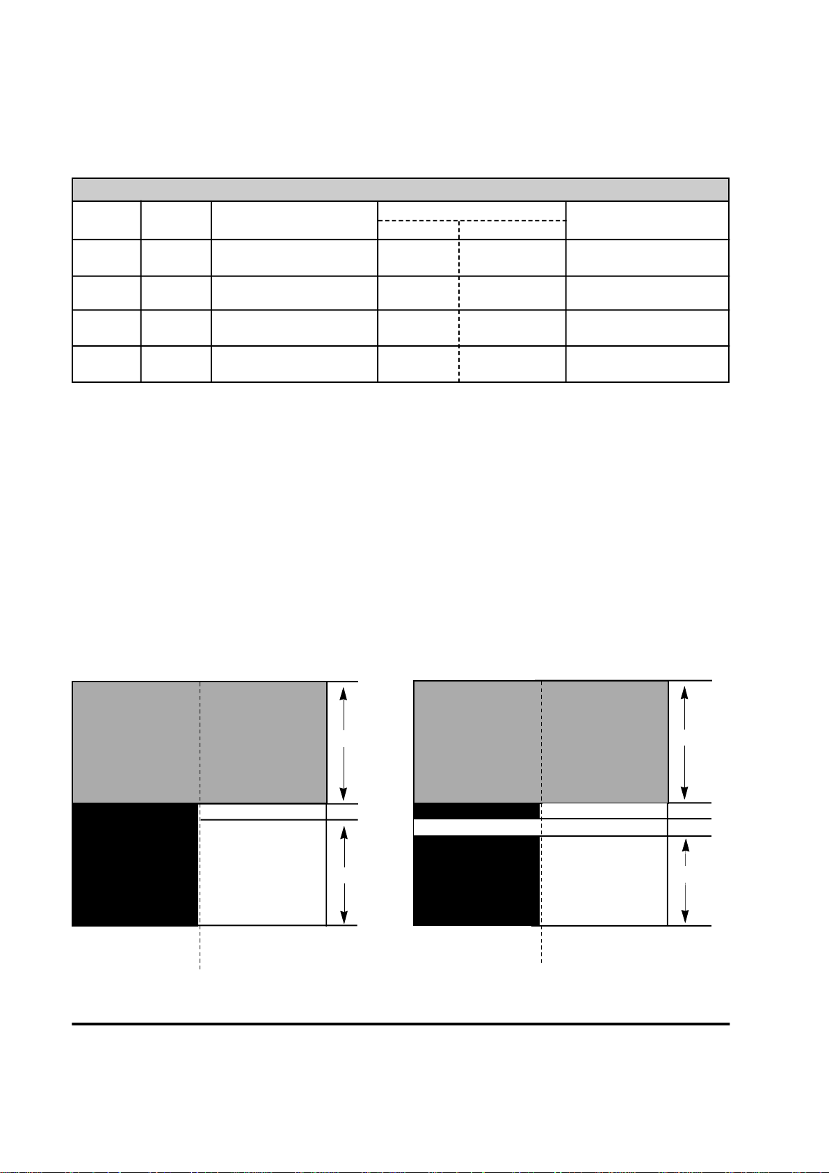
Xecom based the memory structure of the TeleController on the 8051 micro-controller. The lower
32 Kbyte memory addresses include separate
program and data storage. Program and data
storage overlap in the upper 32 Kbytes of memory.
The XE5224DM and XE5224FD Tele-Controllers
have 32 Kbytes of ROM, 32 Kbytes of RAM and
128 Kbytes of Flash memory. ROM contains the
code for Tele-Controller operation and software
design tools; RAM provides space for data storage
by the application program; the 128 Kbytes of Flash
memory can store data and/or application programs.
Flash memory is divided into four, 32 Kbyte pages.
Memory mapping permits shuffling ROM and Flash
memories within the standard 8051 memory
structure. Reconfiguring the Tele-Controller's
memory creates two modes of operation. In
development mode the code in ROM runs the
system. In application mode the application stored
in Flash memory operates the system.
Memory Mapping:
The Tele-Controller insures maximum flexibility with
a configurable memory mapping scheme. Three
external configuration pins select how the memory is
to be used. These three configuration pins, CNFG0,
CNFG1, and CNFG2, can be controlled by output
pins of the XE5224 or by board-mounted jumpers or
switches.
Development Mode:
Develoment mode uses the lower 32 Kbytes of
embedded ROM as program memory. ROM
addresses are 0 to 7FFFF. The lower 32 Kbytes of
data memory are dedicated to RAM except for the
small portion reserved for I/O lines. RAM provides
the Data memory for addresses 0 to 7EFF.
Addresses 7F00 to 7FFF serve peripheral I/O lines.
The upper 32 Kbytes of memory, addresses 8000 to
FFFF, access one of the four pages of Flash
memory. The CNFG1 and CNFG2 configuration
lines selects which page of Flash memory is
addressed. Table 1 shows Tele-Controller memory
mapping in development mode.
Application Mode:
In the application mode a page of Flash memory
serves as the lower 32 Kbytes of program memory.
This page of Flash memory is write protected. As
in the development mode, RAM provides the Data
storage in addresses 0 to 7EFF. Addresses 7F00 to
7FFF are provided for peripheral I/O lines.
The upper 32 Kbytes of memory, addresses 8000 to
FFFF, access page 1 or 3 of Flash memory. If the
application program is stored in either of these
pages, the user may choose to write protect this
page of memory as well. CNFG1 and CNFG2
configuration lines select Flash memory pages and
write protection as shown in Table 2 on the following
page.
Program Memory Data Memory Program/Data
CNFG2 CNFG1 0 - 7FFF 0 - 7EFF 7F00 - 7FFF 8000 - FFFF
0 0 ROM RAM Peripheral I/Os Flash Memory, Page 0
0 1 ROM RAM Peripheral I/Os Flash memory, Page 1
1 0 ROM RAM Peripheral I/Os Flash memory, Page 2
1 1 ROM RAM Peripheral I/Os Flash memory, Page 3
Table 1 Development Mode Memory Mapping (CNFG0=0)

XECOM (6) XE5224DM & XE5224FD
Tele-Controller Memory Configuration continued
Program Memory Data Memory Program/Data
CNFG2 CNFG1 0 - 7FFF 0 -7EFF0 7F00 - 7FFF 8000 - FFFF
0 0 Flash Memory, Page 0 RAM Peripheral I/Os Flash Memory, Page 1
(write protected)
0 1 Flash Memory, Page 0 RAM Peripheral I/Os Flash Memory, Page 1
(write protected) (write protected)
1 0 Flash Memory, Page 2 RAM Peripheral I/Os Flash Memory, Page 3
(write protected)
1 1 Flash Memory, Page 2 RAM Peripheral I/Os Flash Memory, Page 3
(write protected) (write protected)
Table 2 Application Mode Memory Mapping (CFG0=1)
Overlapped Memory:
Data and Program memory share the upper half of
the available memory, addresses 8000 to FFFF.
This area can be accessed as either Program or
Data memory. When downloading Program code
into the XE5224, the code must be stored as Data in
addresses 8000 to FFFF. When the download is
complete, you can access this code as Program
memory because of the memory overlap.
Flash memory may store both user data and the
application program; however, because all pages of
Flash memory are physically located in one device,
you cannot simultaneously read and write from
Flash memory. When the application program must
manipulate stored data, a portion of RAM must be
used as program memory. Memory locations
locations 7E00 to 7EFF overlap RAM and Flash
memory in the Application mode. Reserve these
memory locations for subroutines which require
manipulation of the stored data.
SRAM
(32K)
Program Data
Memory Memory
EPROM
(32K)
Development Mode
8000 - FFFF
Program & Data
Memory Overlap
(32K)
Flash Memory Page 1, 2, 3 or 4
0 - 7EFF
Reserved for Peripheral I/0
SRAM
(32K)
Program Data
Memory Memory
Flash Memory
Page 0 or 2
(32K)
Application Mode
8000 - FFFF
Program & Data
Memory Overlap
(32K)
Flash Memory Page 1 or 3
0 - 7DFF
Reserved for Peripheral I/0
RAM Overlap Addresses 7E00 to 7EFF
Memory Overlap

ROM:
Tele-Controller ROM holds the TC-Monitor and
Tele-Monitor programs to assist in application
development. These programs operate only in
Development mode. These design tools permit the
user to down-load his application program to Flash
memory from either the embedded modem or Serial
Port, edit Flash memory contents, run Analog/Digital
conversions, set and display the Real-Time Clock,
and execute the application program. TC-Monitor
and Tele-Monitor operations are described in detail
elsewhere in this data sheet.
RAM:
32 Kbytes of RAM are primarily used for data
storage by the application program. The
addressable range is from 0 to 7EFF. Addresses
7E00 to 7EFF overlap with program memory in the
Application mode. These locations should be used
for subroutines which need to access data stored in
Flash memory. Addresses 7F00 to 7FFF are
reserved for peripheral I/O use in both Development
and Application mode.
Flash:
Flash memory provides 128 Kbytes of non-volatile
storage for data and/or application programs. Flash
memory is divided into four, 32 Kbyte pages to fit in
the 8051 memory structure. The 128 Kbytes of
Flash memory are contained in one memory chip
within the XE5224.
In Development mode Flash memory is addressed
as the upper 32 Kbytes of overlapped memory,
addresses 8000 to FFFF. The CNFG1 and CNFG2
control lines determine which page of Flash memory
is being addressed.
In Application mode program code may be stored in
any page or pages of Flash memory. Data may be
stored only in Flash memory pages 1 and 3. Again
CNFG1 and CNFG2 control the configuration of
Flash memory. Pages of Flash Memory used for
program storage are write protected.
XE5224DM & XE5224FD (7) XECOM
Tele-Controller Memory Configuration continued
 Loading...