XECOM XE1212C Datasheet

XECOM XE1212C
1200bps Modem Module with Parallel Host Interface
XE1212C
6/97
xecom
Features
•
Small Size -2.28" x 1.0" x 0.5"
• FCC Part 68 Registered
• 212A/103 and CCITTV.22/V.21 Compatible
• Industry Standard "AT" Command Set
• Parallel Interface Emulates 8250B UART
• Call Progress Monitoring
• DTMF and Pulse Dialing
• Software Controlled Audio Output
• Modem Configuration storage in NVRAM
• +5 Volt Power Only
Typical Operating Power 200 mW
Automatic Sleep mode when idle reduces power
consumption to only 50 mW.
Description
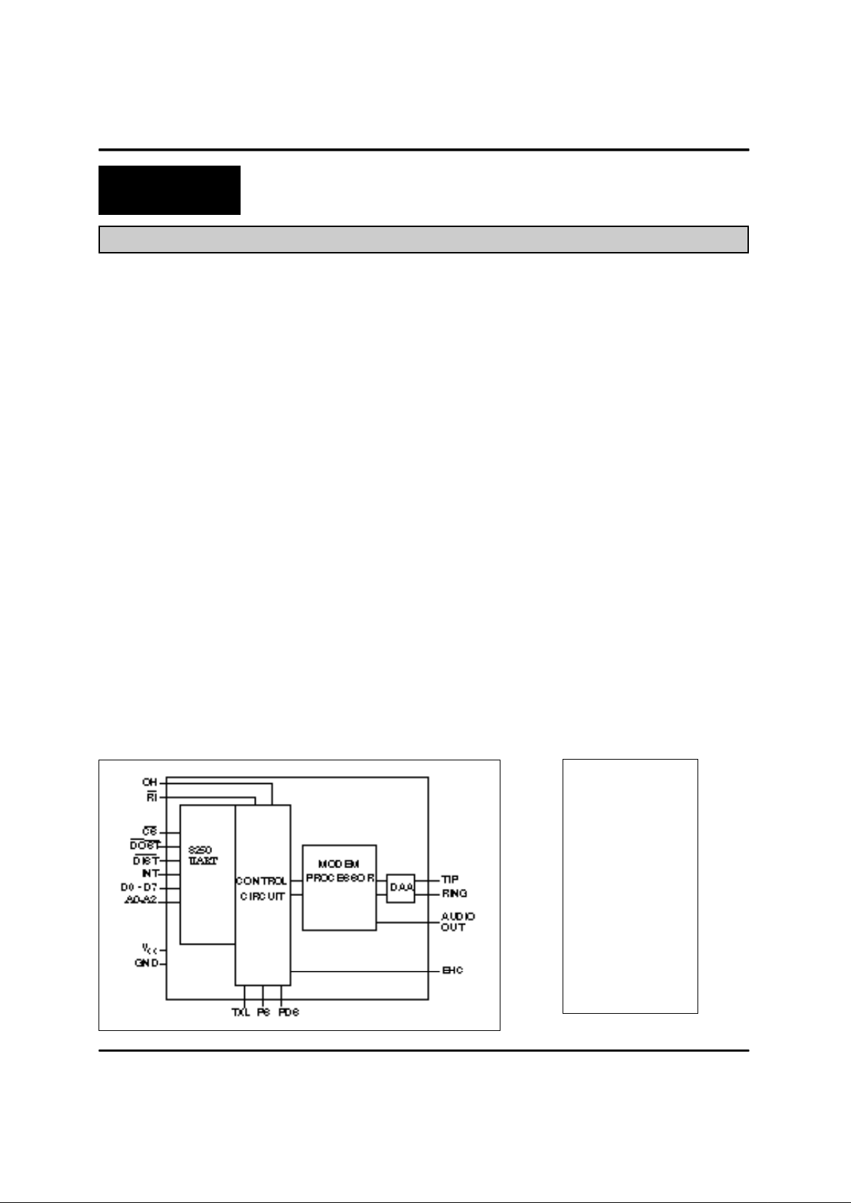
The XE1212C is a complete 1200/300 bps
Modem in a compact, component form factor. It
contains all circuitry necessary for complete
modem functionality, including an FCC Part 68
Registered Data Access Arrangement (DAA) for
direct connection to the telephone line, and a
parallel 8250B UART interface for direct operation
with the IBM-PC, XT or AT system bus. It
operates from the industry standard 'AT'
command set. The XE1212C contains all signal
processing functions, including the modulators
and demodulators for both PSK and FSK
operation, and analog filters.
The XE1212C includes the capability for call
progress monitoring and DTMF tone generation
as well as the guard tones handling required for
CCITT V.22/V.21 communications. It operates in
the asynchronous mode and provides analog
loopback, digital loopback and remote digital
loopback functions for testing.
Block Diagram
1 • 40
2
3
4 37
5
6
7
8
9
10
11
12
13 28
14 27
15 26
16 25
17 24
18 23
19 22
20 21
N/C
GND
Vcc
RI\
N/C
N/C
N/C
N/C
OH
N/C
N/C
AUDIO
INT
A0
A1
A2
CS\
DOST\
DIST\
EHC
TIP
RING
D0
D1
D2
D3
D4
D5
D6
D7
PIN CONFIGURATION

XECOM (2) XE1212C
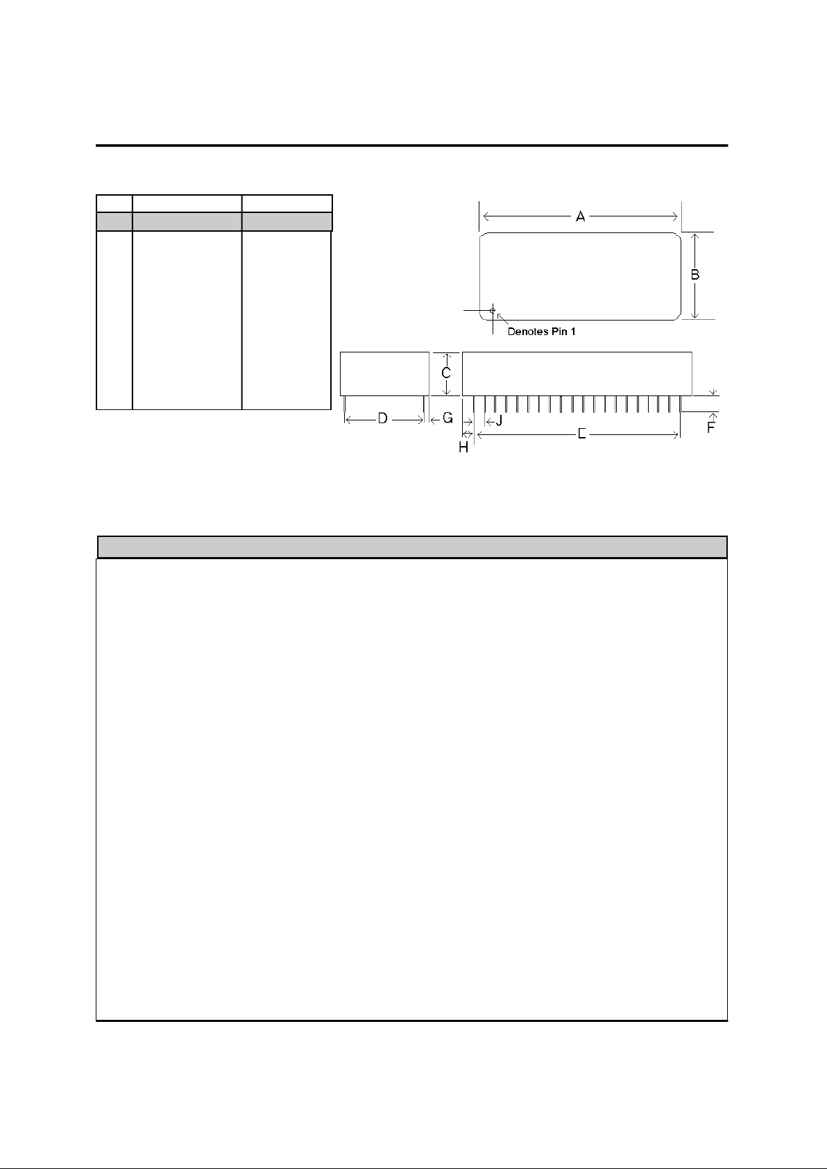
Mechanical Specifications
Pins = 0.020" X 0.014"
All pins tin-plated
Recommended hole size = 0.045"
A 2.255 2.305 57.2 58.6
B 0.985 1.015 25.0 25.8
C 0.490 0.510 12.4 13.0
D 0.890 0.910 22.6 23.1
E 1.890 1.910 48.0 48.5
F 0.125 0.200 3.1 5.1
G 0.040 0.060 1.0 1.5
H 0.180 0.200 4.5 5.1
J 0.090 0.110 2.3 2.8
Inches Milimeters
Min Max Min Max
PIN NAME DESCRIPTION
Pin Descriptions
1 N/C No Connect.
2 GND Ground Reference (0 volts).
3 VCC Positive Supply Voltage (+5 volts).
4 \RI Ring Indication. A low level on this status line indicates the presence of the ring cycle on
Tip and Ring. This line is normally used for test/status only.
5,6,7,8 N/C No Connect
9 OH This signal allows the user to monitor the status of the hookswitch relay in the XE1212C.
When the signal on OH is high, the relay is closed, and the XE1212Csiezes the telephone
line. During rotary dialing, this line is pulsed at a rate of 10 pulses per second.
10,11 N/C No Connect
12 AUDIO A programmable attenuator that can drive a load impedance of 300 ohms is provided on
this pin to allow monitoring of the telephone line signal through an external speaker. The L
and M commands adjust speaker volume and control when the audio signal will be
presented. The Audio Output in conjunction with an external audio amplifier (such as an
LM386) can drive a low impedance speaker.
13 INT The Interrupt Line goes high whenever any of the enabled interrupts in the Interrupt Enable
Register (IER) is active. The interrupts are Received Data Available, Transmitter Holding
Register Empty, Receiver Line Status and Modem Status. The Interrupt Line is reset upon
the appropriate interrupt servicing. This pin is forced to a Hi-Z state when bit 3 bit of the
modem control register (MCR) is low (power on state).
14-16 A0..A2 These 3 address inputs select a UART register during read or write operations as shown in
Table 1. The Divisor Latch Access Bit (DLAB) of the LCR register must be set high by the
system software to access the bit rate Divisor Latch (DLM) as shown in Table 2.

XECOM (3) XE1212C
17 \CS The XE1212C is selected when Chip Select is driven low. When high, the data bus lines
(D0..D7) will be in the high impedance state.
18 \DOST The CPU can write data or control words into a selected register of the XE1212C when
DOST and CS are low. Data is latched on the rising edge of the signal.
19 \DIST The CPU can read data or status from a selected register of the when DIST and CS are
low.
20 EHC External Handset Control. This pin is used to control an additional relay to connnect a
telephone handset to the telephone line. During data transmission, when the internal relay
in the DAA is closed (off hook), this pin is high. When the internal relay is open (on-hook),
this pin is low and may be used to close an external relay to connect the telephone handset
to the line.
21-28 D7-D0 This eight bit data bus provides bidirectional communications between the modem and
CPU. Data, Control words and Status information are transferred on these bus lines.
These are tri-state lines and have internal drive buffers eliminating the need for external
buffering between the CPU bus and the XE1212C.
37,40 RING/TIP These are the TIP and RING connections to the telephone line from the DAA. In order to
maintain the high voltage isolation provided by the DAA, traces from these pins to the
RJ11C Jack should have a minimum spacing of 100 mils between them and any other
traces on the board.
PIN NAME DESCRIPTION
Pin Descriptions
ABSOLUTE MAXIMUM RATINGS*
SUPPLY VOLTAGE - Vcc +6 Volts
DC INPUT VOLTAGE -0.6 Volts to (Vcc +0.6 Volts)
STORAGE TEMPERATURE RANGE -25° C TO +85° C
LEAD TEMPERATURE 260° C
(Soldering, 2 seconds per wave)
OPERATING TEMPERATURE RANGE 0 TO 70° C
*Exceeding these values may result in permanent damage to the device.

XECOM (4) XE1212C
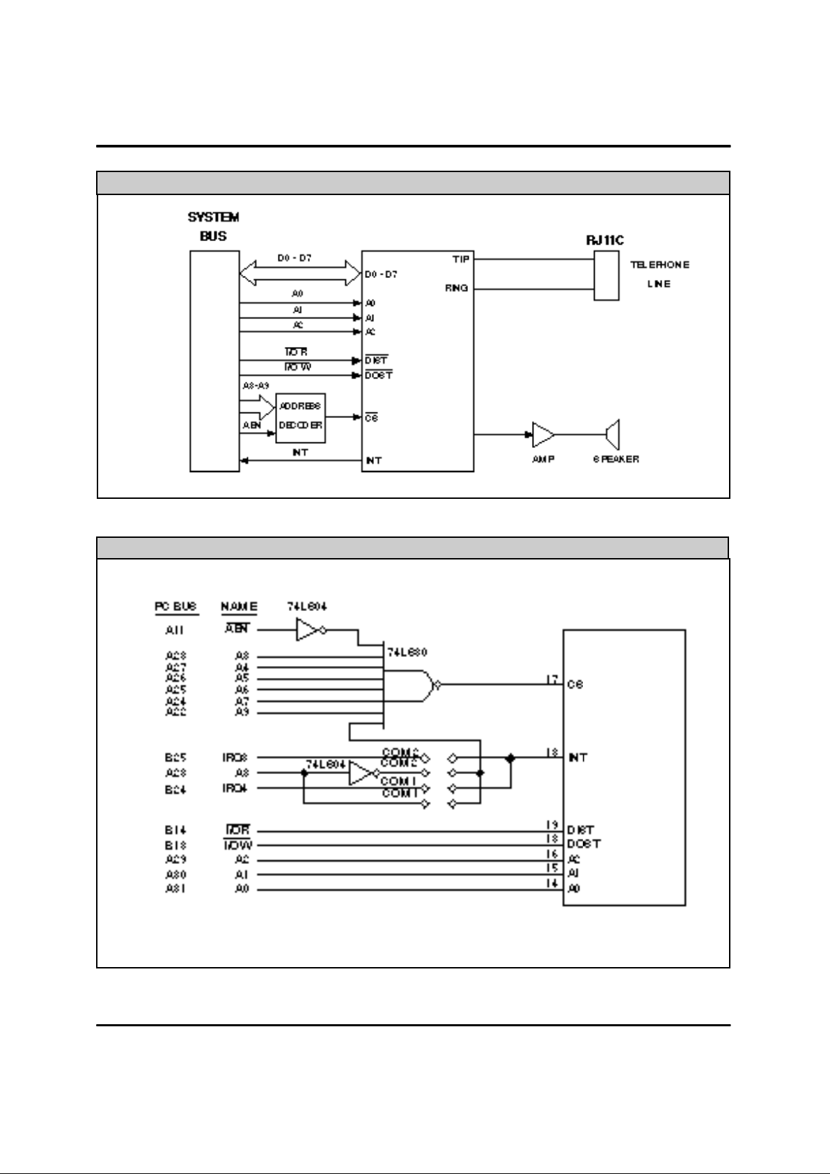
IBM-PC Bus Interface Address Decoder
XE1212C
Typical Connection Diagram
XE1212C

XECOM (5) XE1212C
0 0 1 2 3 4 5 6 0 1
(DLAB=0) (DLAB=0) (DLAB=0) (DLAB=1) (DLAB=1)
Transmit
Set Shift Ring
6 Data Bit Data Bit 0 0 Break 0 Register Indicator Bit 6 Bit 14
6 6 1=SB Empty (RI)
(TSRE)
Receiver Transmitter Interrupt Interrupt Line Modem Line Modem Divisor Divisor
Bit Buffer Holding Enable Indent. Control Control Status Status Latch Latch
No. Register Register Register Register Register Register Register Register (DLL) (DLM)
(RBR) (THR) (IER) (IIR) (LCR) (MCR) (LSR) (MSR)
Enable "0" if Word Length Data
0 Data Bit Data Bit RXD Interrupt Selection Terminal Data Delta Bit 0 Bit 8
0* 0* Available Pending Bit 0 Ready Ready CTS
Interrupt (DTR)
Enable
Transmitter Interrupt Word Length Request Overrun Delta
1 Data Bit Data Bit Holding Ident. Selection to Send Error DSR Bit 1 Bit 9
1 1 Reg. Empty Bit 0 Bit 1 (RTS) (OE)
Interrupt
Enable Trailing
Receiver Interrupt Stop Bits Output 1 Parity Edge
2 Data Bit Data Bit Line Status Ident. 0=1 SB Error Ring Bit 2 Bit 10
2 2 Interrupt Bit 1 1=2 SB (PE) Indicator
Enable Parity Framing Delta
3 Data Bit Data Bit Modem 0 Enable Output 2 Error Rx Line Bit 3 Bit 11
3 3 Status 1=PEN (FE) Signal
Interrupt Detect
4 Data Bit Data Bit 0 0 Even Parity Local Break Clear to Bit 4 Bit 12
4 4 Select Loopback Interrupt Send
1=EPS (CTS)
Stick Transmit
5 Data Bit Data Bit 0 0 Parity 0 Holding Data Set Bit 5 Bit 13
5 5 1=SP Register Ready
Empty (DSR)
(THRE)
Divisor Received
Latch Line
7 Data Bit Data Bit 0 0 Access 0 0 Signal Bit 7 Bit 15
7 7 Bit Detect
(DLAB)
UART Register Function Summary
Register Address
*Bit 0 is the least significant bit. It is the first bit serially transmitted or received.
 Loading...