WTE P6SMBJ User Manual

查询P6SMBJ13CA供应商查询P6SMBJ13CA供应商
WTE
POWER SEM ICOND UCTOR S
P6SMBJ SERIES
600W SURFACE MOUNT TRANSIENT VOLTAGE SUPPRESSORS
Features
!
Glass Passivated Die Construction
!
600W Peak Pulse Power Dissipation B
!
5.0V – 170V Standoff Voltage
!
Uni- and Bi-Directional Versions Available D
!
Excellent Clamping Capability A
!
Fast Response Time F
!
Plastic Case Material has UL Flammability
Classification Rating 94V-O C H G
Mechanical Data
!
Case: JEDEC DO-214AA Low Profile Molded Plastic
!
Terminals: Solder Plated, Solderable
per MIL-STD-750, Method 2026
!
Polarity: Cathode Band or Cathode Notch
!
Marking:
Unidirectional – Device Code and Cathode Band
Bidirectional – Device Code Only
!
Weight: 0.093 grams (approx.)
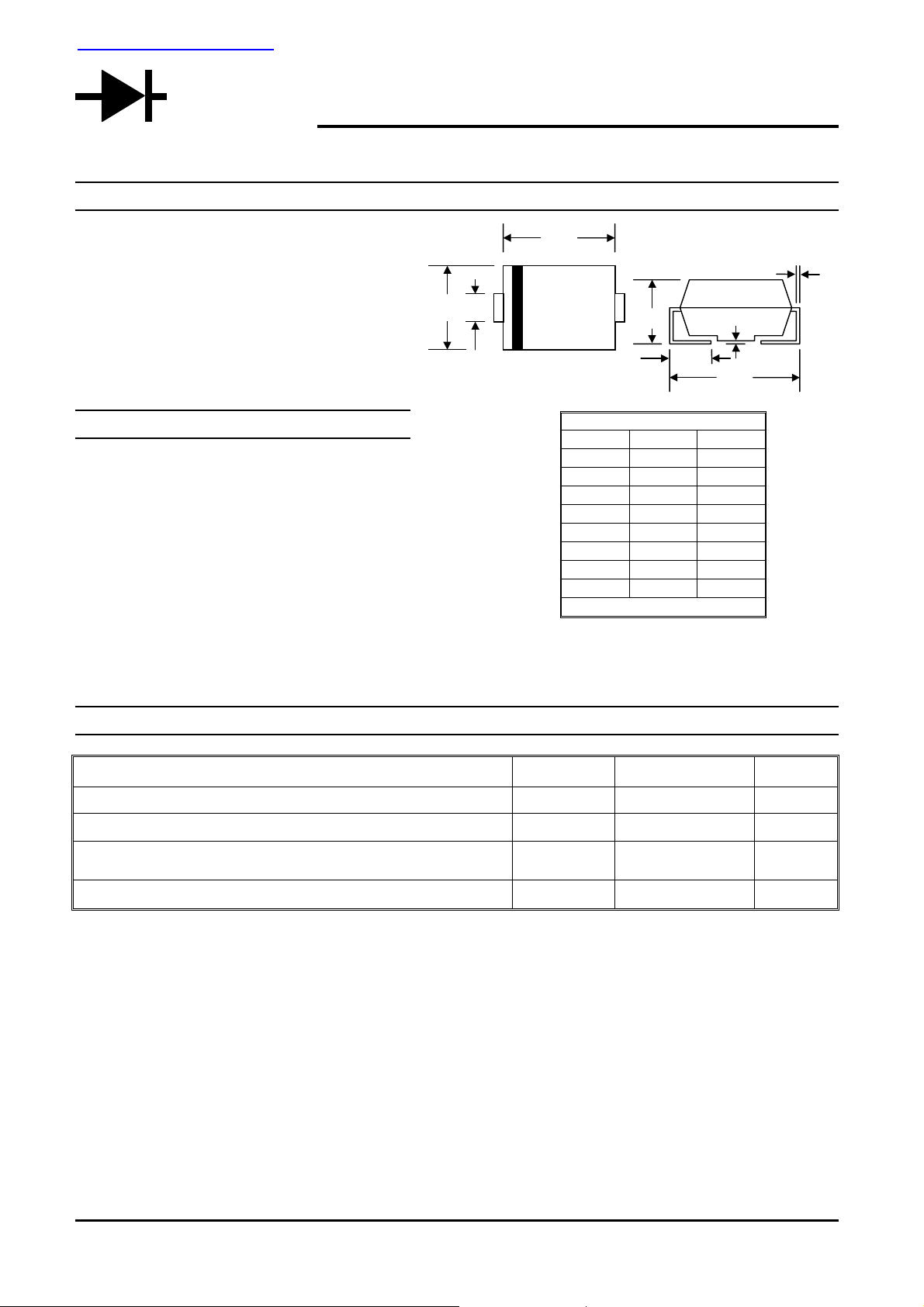
SMB/DO-214AA
Dim Min Max
A
B
C
D
E
F
G
H
All Dimensions in mm
3.30 3.94
4.06 4.70
1.91 2.11
0.152 0.305
5.08 5.59
2.13 2.44
0.051 0.203
0.76 1.27
E
“C” Suffix Designates Bi-directional Devices
“A” Suffix Designates 5% Tolerance Devices
No Suffix Designates 10% Tolerance Devices
Maximum Ratings and Electrical Characteristics
Characteristic Symbol Value Unit
Peak Pulse Power Dissipation 10/1000µS Waveform (Note 1, 2) Figure 3 P
Peak Pulse Current on 10/1000µS Waveform (Note 1) Figure 4 I
Peak Forward Surge Current 8.3ms Single Half Sine-Wave
Superimposed on Rated Load (JEDEC Method) (Note 2, 3)
Operating and Storage Temperature Range Tj, T
Note: 1. Non-repetitive current pulse, per Figure 4 and derated above TA = 25°C per Figure 1.
2. Mounted on 5.0mm
3. Measured on 8.3ms single half sine-wave or equivalent square wave, duty cycle = 4 pulses per minutes maximum.
2
(0.013mm thick) land areas.
@TA=25°C unless otherwise specified
PPM
FSM
I
PPM
STG
600 Minimum W
See Table 1 A
-55 to +150 °C
100 A
P6SMBJ SERIES 1 of 5 © 2002 Won-Top Electronics

100
75
10000
T = 25 Cj°
50
25
PEAK POWER OR CURRENT
PEAK PULSE DERATING IN % OF
0
10 X 1000 Waveform
as defined by REA
0 25 50 75 100 125 150 175 200
T , AMBIENT TEMPERATURE ( C)
A
°
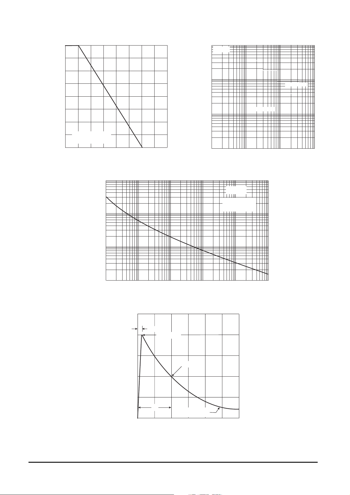
Fig. 1 Pulse Derating Curve
100
10
1.0
d
P , PEAK PULSE POWER (kW)
J
C , JUNCTION CAPACITANCE (pF)
1000
Stand-Off Voltage
100
10
1 10 100 1000
V , STANDOFF VOLTAGE (V)
WM
Fig. 2 Typical Junction Capacitance
T = 25 C
°
j
Non Repetitive
Pulse Waveform
Zero Bias
0.1
0.1 1.0
Ppp
I , PEAK PULSE CURRENT (%I )
10 100
t PULSE WIDTH ( s)
p
µ
Fig. 3 Pulse Rating Curve
t = 10 s
µ
100
r
Peak Value I
pp
Half Value I /2
pp
50
t
p
0
10 X 1000 Waveform
as defined by R.E.A.
012
t, TIME (ms)
Fig. 4 Pulse Waveform
1000 10000
3
P6SMBJ SERIES 2 of 5 © 2002 Won-Top Electronics
 Loading...