

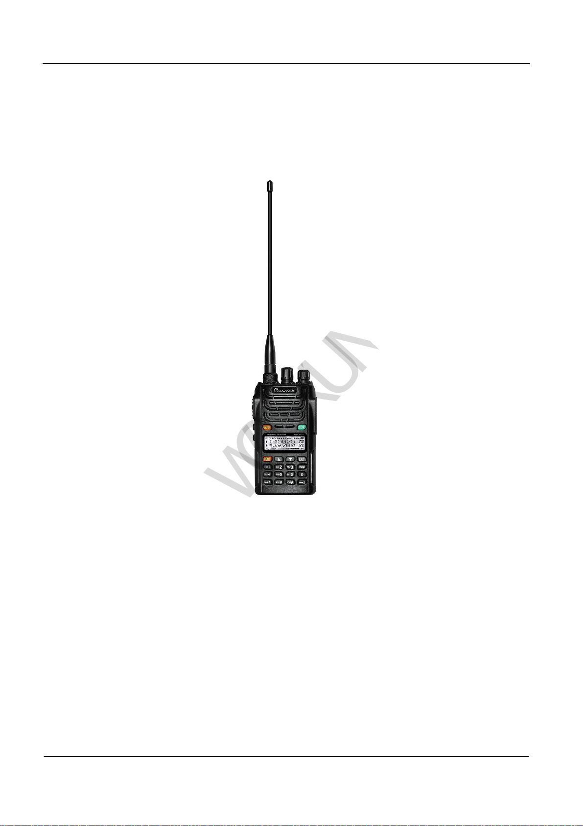
QUANZHOU WOUXUN ELECTRONICS CO., LTD Model: KG-UVD1
WOUXUN
Service Manual
Model: KG-UVD1
Version: KG-UVD1-0905-V1
QUANZHOU WOUXUN ELECTRONICS CO., LTD
Version: KG-UVD1-0905-V1 Page 1 of 43
QUANZHOU WOUXUN ELECTRONICS CO., LTD Model: KG-UVD1
WOUXUN
KG-UVD1 Dual-Band Maintenance Manual
Introduction
The Scope for the Manual
This manual is for the technicians who know well about the communication and have some experiences of
maintenance. All necessary information of maintenance and actual published date are included in this manual.
If there is any change after publishing, we will complement it by “Maintenance Aviso” or “Manual Revision”
according to the requirements.
Personal Safety
● Please pay attention to the below proceedings for your safety:
Don’t transmit before you carefully check all plugs for TX Frequency, or any of the unfolded plugs doesn’t
connect to the relative ends.
● Please turn off the power, and don’t operate the equipment when you are near the electric detonator or on
flammability gas station.
●Only the qualified technicians can maintain the equipment.
Maintenance Service
In order to maintain the equipment easily and establish the complete maintenance system, we supply the information
including principium chart, printing circuitry chart and the settings of the equipment.
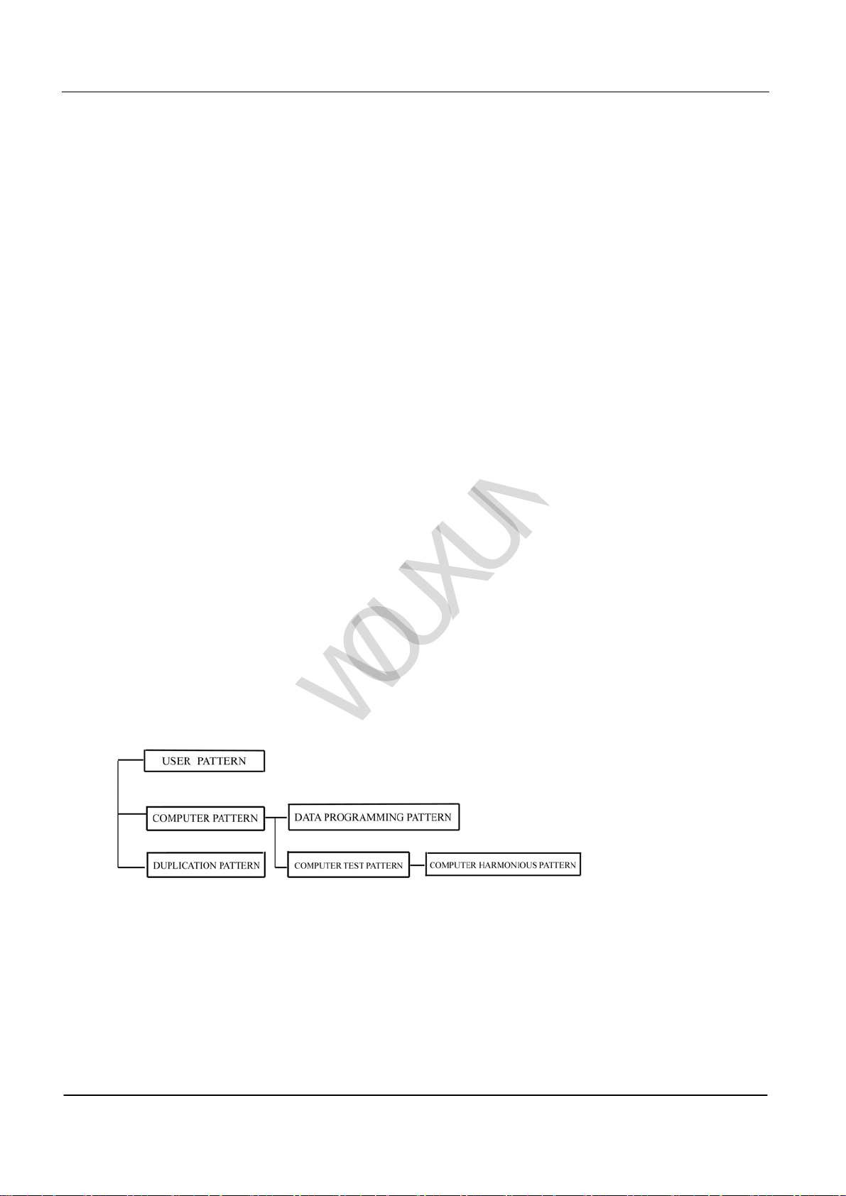
Mode Combination
1. Mode Combination
Version: KG-UVD1-0905-V1 Page 2 of 43
QUANZHOU WOUXUN ELECTRONICS CO., LTD Model: KG-UVD1
WOUXUN
2.Enter the Mode
3.Computer Mode
KG-UVD1 handheld transceiver programs by computer, the programming connection and the programming software
(KG-UVD1). The programming software can be used in the IBM computer or compatible machine.
Duplication Mode
1. “Duplication Mode” can copy the data of a handheld transceiver to another one.
The dealers can do this duplication without a personal computer.
2. Operating Method
①Connectting the duplicated source radio with waiting-duplicated target radio by cloning Line
(The waiting-duplicated target radio need to be putting through the power source)
Version: KG-UVD1-0905-V1 Page 3 of 43
QUANZHOU WOUXUN ELECTRONICS CO., LTD Model: KG-UVD1
WOUXUN
○2Pressing [MONI] key on duplicated source radio, the duplication starts.
When duplicating, the flickering red light means sending data. After duplicating successfully, the red light
extinguishes, and the source radio enters the standby mode. If the red light keeps flickering, it means the duplication
failed.
The green light flickers when the target radio duplicates. The duplication finishes when the green light extinguishes.
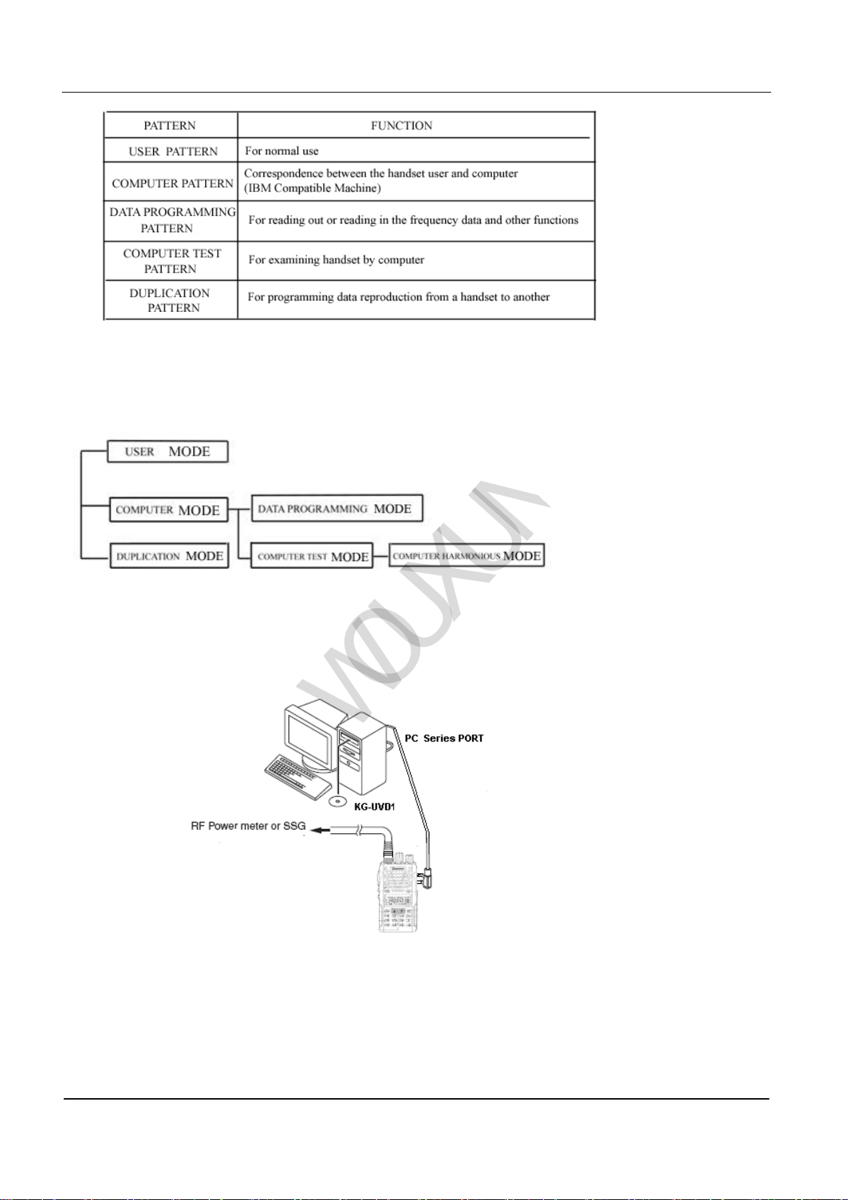
Assembling & Dissembling Chart
Disassembling Shell Chart Disassembling TX/RX Board Chart
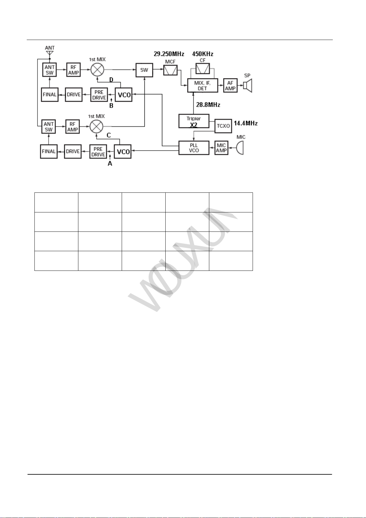
ⅠFrequency Structure
Version: KG-UVD1-0905-V1 Page 4 of 43
QUANZHOU WOUXUN ELECTRONICS CO., LTD Model: KG-UVD1
WOUXUN
Pic 1
Frequency
Structure
(1) 136~
(2) 136~
(3) 136~
Chart 1
Please refer the frequency of A.B.C.D points of PIC 1 on Chart 1.
st
intermediate frequency of this radio is 29.250MHz, the 2nd is 450KHz.
The 1
A C B D
174.995MHz
174.995MHz
174.995MHz
165.250~
204.245MHz
165.250~
204.245MHz
165.250~
204.245MHz
400~
470.995MHz
450~
520.995MHz
245~
245.995MHz
429.25~
500.245MHz
479.25~
550.245MHz
274.25~
275.245MHz
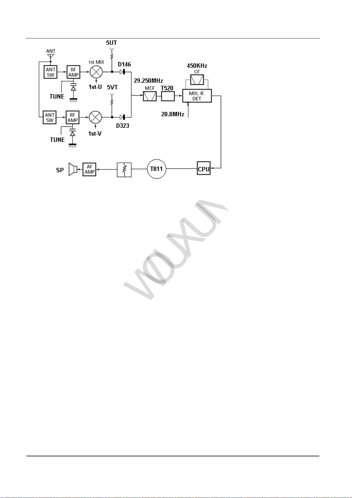
Ⅱ Receiving
(1) The front end of U Band (RF Amplifier)
The signal which is received from the antenna enters the transmission/receive change-over switch diode circuit
(D148, D137, D138 and D147), then goes through BPF (L191 and L192), and is enlarged by RF amplifier (T322).
The signal goes through the BPF(L185,L189,L187,L188), and then enters the mixing. These BPF (D142, D143,
D144, D145) is adjusted by the variable condenser. The input voltage by variable condenser is adjusted by the
outputting voltage by microprocessor (IC811).( See PIC 2)
(2)The front end of V Band(RF Amplifier)
The signal which is received from the antenna enters the transmission/receive change-over switch diode circuit
(D322,D315,D316 和 D443), then goes through BPF(L344 and L345), and is enlarged by RF amplifier (T324).The
signal goes through the BPF(L320,L342,L341 L340), and then enters the mixing. These BPF (D318
D319, D320,D321)adjusted by the variable condenser. The input voltage by variable condenser is adjusted by the
outputting voltage by microprocessor (IC811).( See PIC 2)
Version: KG-UVD1-0905-V1 Page 5 of 43
QUANZHOU WOUXUN ELECTRONICS CO., LTD Model: KG-UVD1
WOUXUN
图2 PIC2
(3) The 1st Mixer
The signals from the front end of U Band and the Rx LO prouduced by PLL electrocircuit creat the 1st immediate
frequency signal of 29.250MHz on T144 Mixing. The created signal is sent to the changeover on-off on U/V Band.
st
The signals from the front end of V Band and the Rx LO prouduced by PLL electrocircuit creat the 1
frequency signal of 29.250MHz on T323 Mixing. The created signal is sent to the changeover on-off on U/V Band.
The changeover on-off switches the signals according to the working state of U/V Band on microprocessor (IC811).
After switching, the signals are sent to MCF(FL515,FL516) (See PIC2)
(4)
The first signal from intermediate frequency eliminate the signals from adjacent channels through
MCF(FL515,FL516). The amplifier (T520) enlarges and enters the I-F system chip (U516). The I-F system chip
provides the second mixer, the second LO signal, limiting amplifier, orthogonal detector and RSSI (received signal
intensity indicator).The second mixer sends and mixes the first intermediate frequency signal and the second LO
signal of 28.8MHz, and then creates the second LO signal of 450kHz.
The second intermediate frequency signal keeps eliminating the signals of the adjacent channels by the chinaware
wave filter. The second signal through filter is enlarged by limiting amplifier and demodulated by orthogonal detector
with chinaware discriminator. The demodulated signal enters the tone circuit on microprocessor (IC811) and
processes.(See PIC2)
The enlarging circuit on Intermediate Frequency
immediate
(5)
Version: KG-UVD1-0905-V1 Page 6 of 43
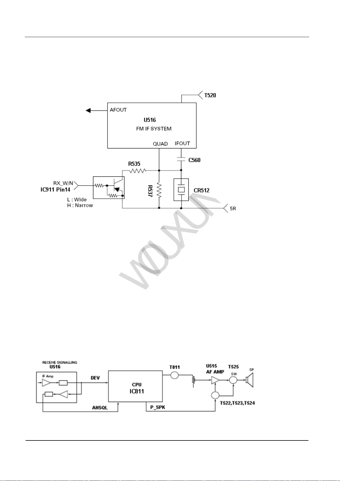
Wide/Narrow Switch Circuit
QUANZHOU WOUXUN ELECTRONICS CO., LTD Model: KG-UVD1
WOUXUN
We can set the bandwidth of all channels by turning on the Wide/Narrow switch.
th
The data from Wide (low level) and Narrow (high level) is outputted by the 14
T528 is connected when receiving the data from WIDE (low level).
T528 is disconnected when receiving the data from NARROW (high level).
T528 is connected/ disconnected by WIDE/NARROW data.The regular changing level from U516 detector is used to
maintain the constant output level on WIDE/NARROW signals. (See PIC3)
pin on microprocessors.
PIC3
)
(6
The demodulated signal is sent to the tone amplifier by T811 from the 25th feet tube of microprocessor (IC811),after
entering the tone circuit and being processed.
After being enlarged by the tone power amplifier, the signal is outputted to the loudhailer by AF volume control.
(See PIC 2)
(7)
A part of AF signals from FM IC (U516) enter IC again. The noise components are enlarged and revised by the filter,
and then creates the DC voltage corresponded to the noise level.
The DC signal is sent to the simulated port (Pin28) of microprocessor through FM IC. IC405 decides whether
outputs the sound from the speaker by testing the outputted voltage is higher or lower than the default value.
(See PIC4)
Tone Amplifier Circuit
Squelch
PIC4
Version: KG-UVD1-0905-V1 Page 7 of 43
QUANZHOU WOUXUN ELECTRONICS CO., LTD Model: KG-UVD1
WOUXUN
(8)
The signal from FM IC (U516) enters and is processed by microprocessor (IC811).(See PIC4)
Microprocessor (IC811)determin whether QT or DQT matches the setting value, and control the output of P-SPK
and loudhail by this result. (See PIC 4)
Receiving Signaling (QT/DQT)
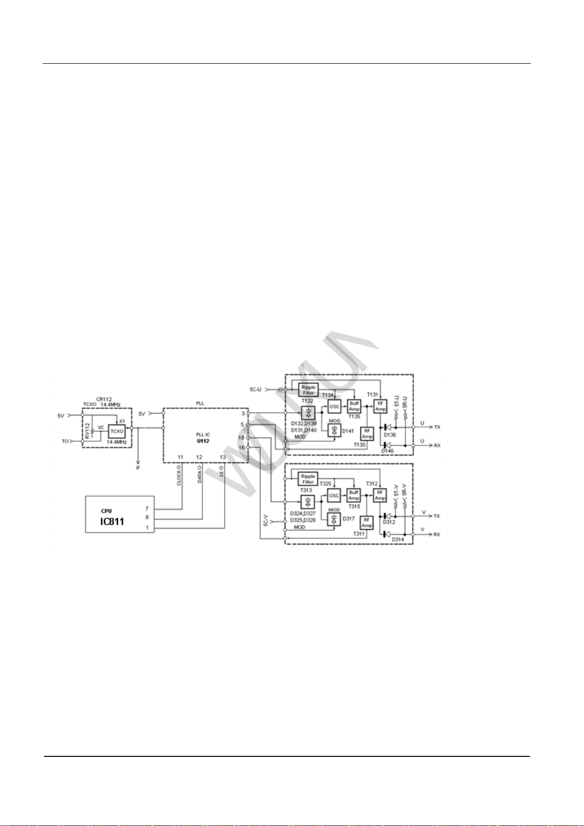
Ⅲ PLL Frequency Syntheses
PLL circuit produces the Rx LO for receiving and the RF signal for transmitting. This transceiver is adopted double
channel integrate circuit, which can simultaneously prod uce tw o different Rx LO and RF signal.
(1) PLL
The frequency step of PLL circuit is 5 or 6.25kHz.
The referring surge signal of 14.4MHz is divided frequency by a fixed arithmometer in U112. The signal from the
oscillator (VCO) is cushioned and enlarged by T130 and T311 separately, and is divided frequency by programmable
double modulation arithmometer separately in U112. In the U112 phase comparator, the frequency division processes
compare. After being filtered by the different lowpass, the two created signals separately are sent to the two
independent VCO controlling frequency of oscillator. See PIC 5
图5 PIC5
(2)VCO
cU Band VCO on the Transceiver
The frequency that is used in U Band on the transceiver is produced by T134 vibration when it is transmitting or
receiving frequency points.
Through the phase comparator will receive transportation to the VCO control voltage variable diode
(D132, D139, D131, D140) to control the oscillation frequency.Oscillation frequency of the signal by
the T135, T135 amplification levels, with the D136 and D135 were sent to the RF amplifiers and
receivers for the first points of the vibration frequency. See PIC5.
d V Band VCO on the Transceiver
The frequency that is used in V Band on the transceiver is produced by T325 vibration when it is transmitting or
Version: KG-UVD1-0905-V1 Page 8 of 43
QUANZHOU WOUXUN ELECTRONICS CO., LTD Model: KG-UVD1
WOUXUN
receiving frequency points.
Through the phase comparator will receive transportation to the VCO control voltage variable diode
(D324, D325, D327, D328) to control the oscillation frequency.Oscillation frequency of the signal by
the T135, T135 amplification levels, with the D136 and D135 were sent to the RF amplifiers and
receivers for the first points of the vibration frequency. See PIC5.
Ⅳ Transmitting Part System
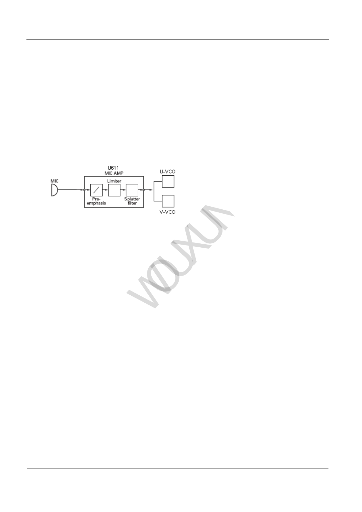
(1) Speaker Amplifier
The signal from speaker processes regulation of the maximum frequency deviation by tone processor (U611). And
then it is sent to VCO on U Band or V Band for modulating and inputting. See PIC 6
` PIC6
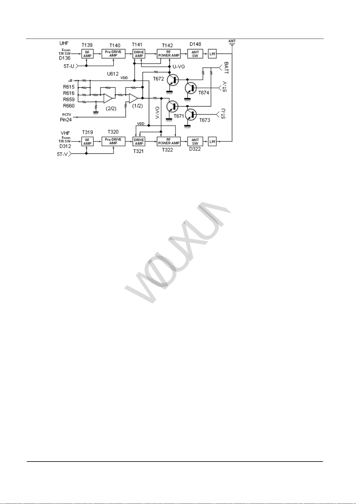
(2)Drives and Terminal Amplifier
This transceiver has two separation drives and terminal amplifiers on U Band and V Band.
cDrives and Terminal Amplifier on U Band
The signal from T/R Switch (D136 ON) is enlarged to 50mW by pre-drive amplifier (T139,T140) and drive amplifier
(T141). The output of drive amplifier is enlarged to 4.0W by the RF power amplifier (T142) (works as when low
power is 1W). The output of RF power amplifier is through the harmonic filter (LPF) and the antenna switch (D148),
and is sent to the terminal of the antenna .
See PIC 7
d Drives and Terminal Amplifier on V Band
The signal from T/R Switch (D312 ON) is enlarged to 50mW by pre-drive amplifier (T319,T320) and drive amplifier
(T322). The output of drive amplifier is enlarged to 4.0W by the RF power amplifier (T322) ((works as when low
power is 1W). The output of RF power amplifier is through the harmonic filter (LPF) and the antenna switch, and is
sent to the terminal of the antenna (D322).
See PIC 7
Version: KG-UVD1-0905-V1 Page 9 of 43
QUANZHOU WOUXUN ELECTRONICS CO., LTD Model: KG-UVD1
WOUXUN
PIC 7
(3)Automatic Power Control Circuit (APC)
APC circuit always monitor the circuit that is through the radio frequency RF amplifier (T142 or T322),and maintain
the stable electric current. The diversification of electronic current that is enlarged by radio frequency power
amplifier can cause the lower voltage of R615, R616, R659 and R660. The voltage is sent to difference amplifier
U612(2/2) U612(1/2), and compares the outputting voltage of IC101(2/2) with the reference voltage from IC405.
The output voltage of U612 (1/2) control the radio frequency RF amplifier, drive amplifier, VG of pre-drive amplifier
to keep the voltage consistent.
The changes of high/low power are realized by changing the reference voltage.
The two terminal amplifiers of this transceiver use the same APC circuit. So they are switched on the
output VG voltage from APC. When U Band transmitting, the VG voltage that sends APC to V Band
resists to ground short circuit. On the contrary, when V Band transmitting, the VG voltage that sends
APC to U Band resists to ground short circuit. See PIC7
(4)
QT/DQT
The DQT/QT data outputs from the CPU 23 base pins. The signal through the low pass CR filter, a partial signal
delivers TCXO CR112. Another part of signal and the tone signaling mix, then inputs separately to U or V Band of
VCO.
Coding Signaling
Ⅴ Electrical Power
10 electrical power of 5V is used in this transceiver.
They respectively provide to the microprocessor: 5V,5M
When connecting, 5M always keep outputting. Although 5M is the regular output,it is closed when turn off the
electrical power to prevent the microprocessor from malfunction.
5C-V is the public 5V on V Band,which keeps output on non-save mode.
5C-U is the public 5V on U Band,which keeps output on non-save mode.
5R-U is the receiving 5V on U Band,which keeps output during receiving.
Version: KG-UVD1-0905-V1 Page 10 of 43
QUANZHOU WOUXUN ELECTRONICS CO., LTD Model: KG-UVD1
WOUXUN
5T-U is the transmitting 5V on U Band,which keeps output during transmitting.
5R-V is the receiving 5V on V Band,which keeps output during receiving.
5T-V is the transmitting 5V on V Band,which keeps output during transmitting.
5R is the shard 5V by the intermediate frequency circuit. (U band and V band of receiving use in common the partial
power source.
The electrical power is used in enlarging the speaker (The shared partial electrical source on U Band and V Band)
There are another two overall electrical sources, BATT+ and BATT.
BATT+ is input electronic source. BATT is electronic source by controlled by power switch.
Ⅵ Controlled Electrical Circuit
The controlled circuit is made up of microprocessor(IC811) and exterior circuit.
It controls the TX-RX unit. The main functions of IC811 are as bellows:
(1) Transforming the transmitting and receiving states according to PTT input signal
(2) Numerating system,group, frequency and program data from the stored circuit
(3) Sending frequency data to PLL
(4) Controlling the open and close of squelch according to the output DC voltage from squelch circuit.
(5) Controlling the tone frequency mute according to the decoding data
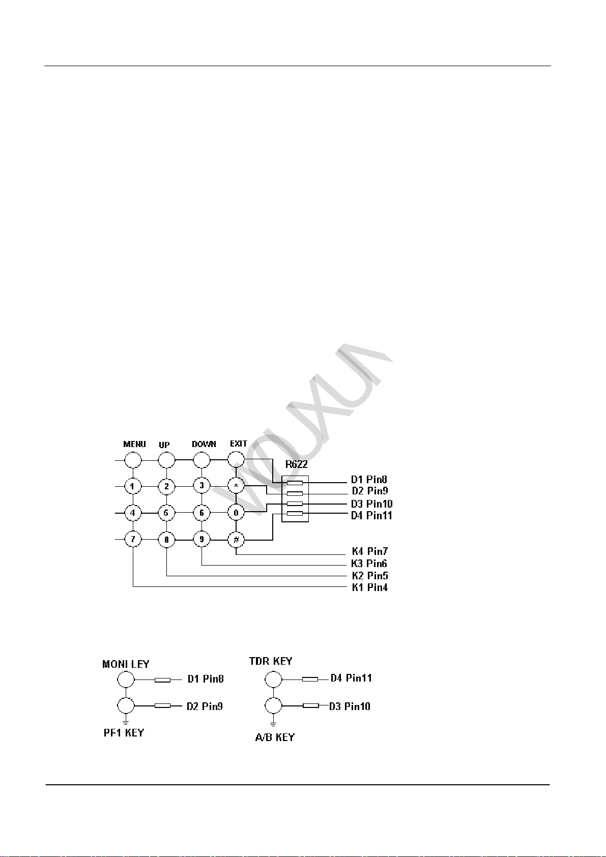
Ⅶ Keypad and display circuit
(1)Keyboard entry examination
K1,K2,K3,K4 are keypad fan-out,D1,D2,D3,D4 are keypad input end. They are managed after examining by
microprocessor (IC811). See PIC8
图8
图9
Version: KG-UVD1-0905-V1 Page 11 of 43
QUANZHOU WOUXUN ELECTRONICS CO., LTD Model: KG-UVD1
WOUXUN
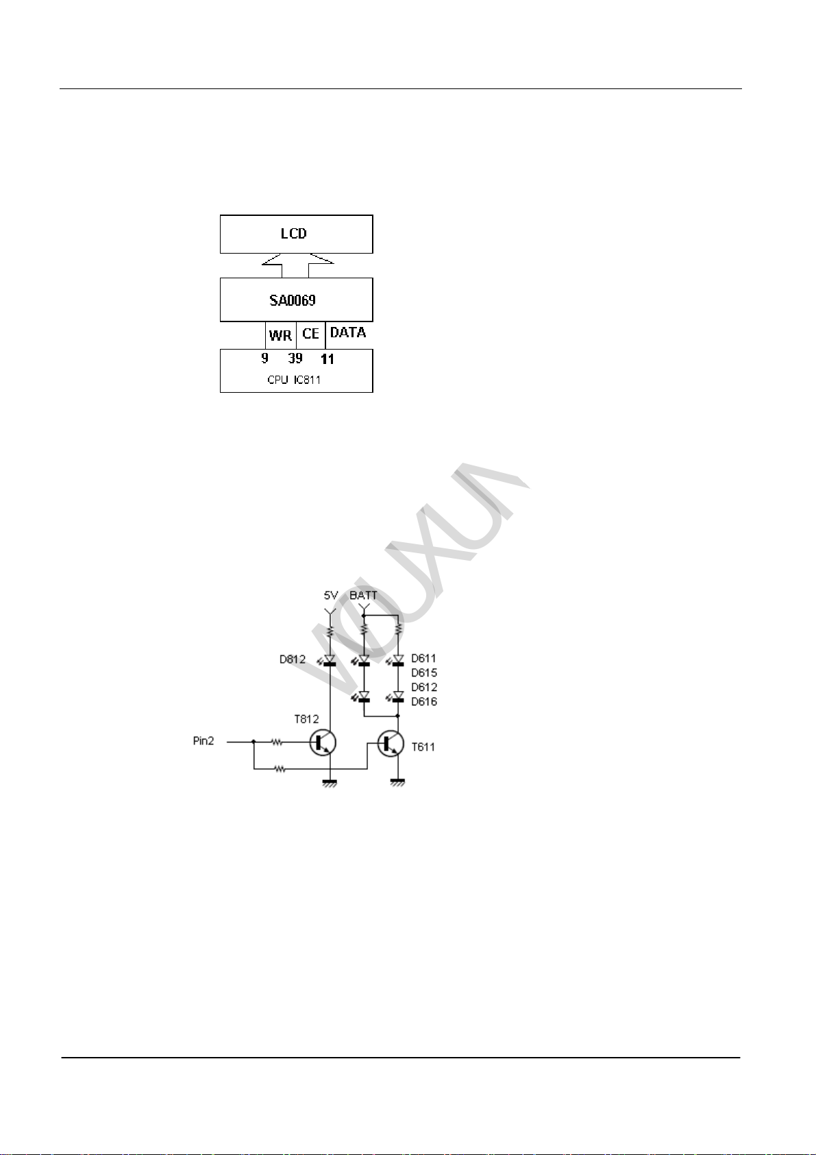
(2) Display Circuit
LCD demonstrated the information (IC811) controls the screen by the microprocessor (liquid crystal) to demonstrate
that the actuation integrated circuit causes the screen (liquid crystal) the monitor demonstration corresponding
information. See PIC 10
PIC10
(3)Backlight Circuit
The backlight of LCD and keypad is single-colored, which is controlled by the pin of microprocessor.
See PIC11
PIC11
(4)Illumination Circuit
The illumination circuit is controlled by the pin of the microprocessor(IC811). See PIC12
Version: KG-UVD1-0905-V1 Page 12 of 43
QUANZHOU WOUXUN ELECTRONICS CO., LTD Model: KG-UVD1
WOUXUN
PIC 12
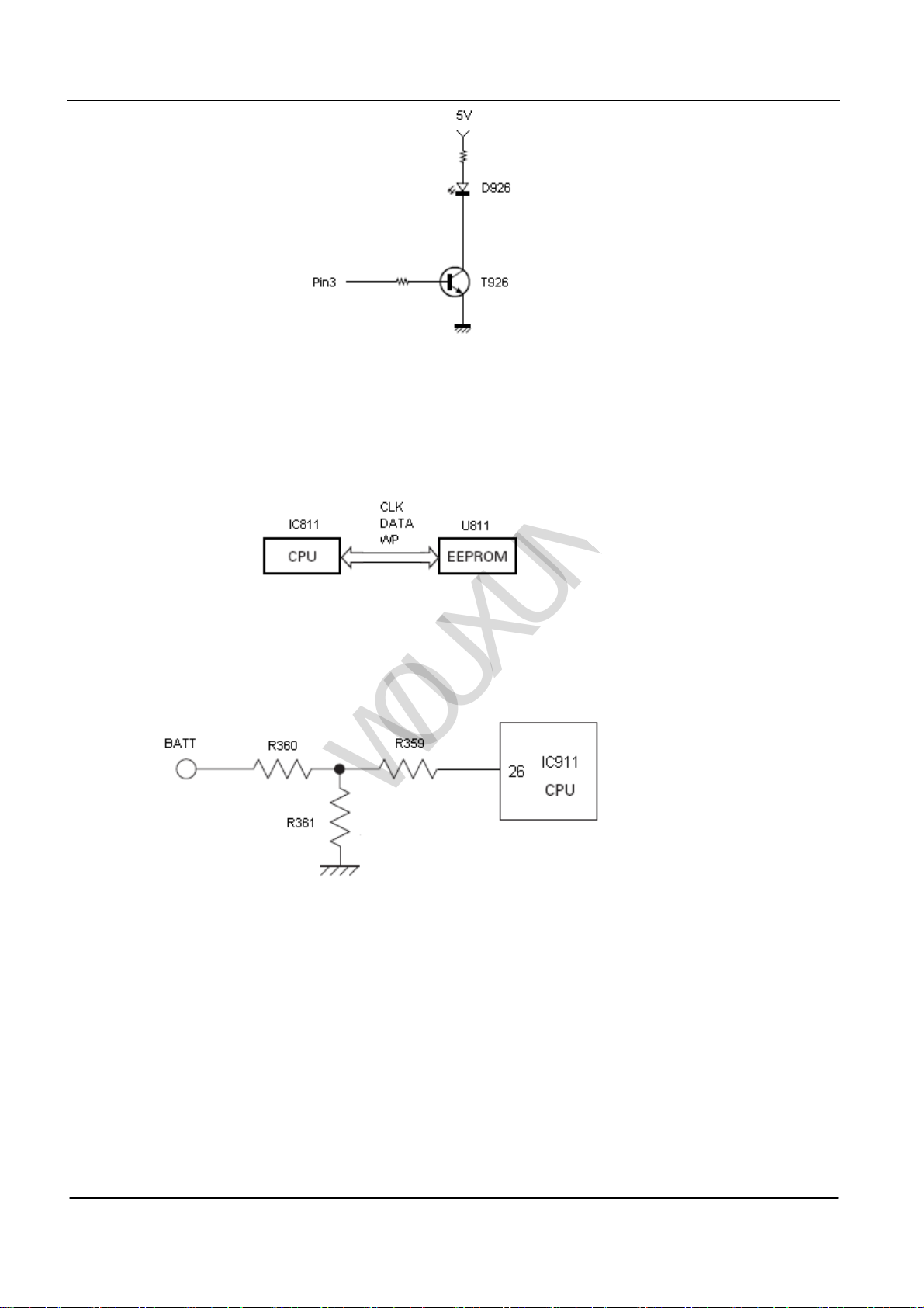
Ⅷ Memorizer Circuit
The memorizer circuit is made up of CCPU (IC811) and EEPROM (U811)
The capacitance is 64k bits, including the handset controlling program by CPU and the operation function data.
See PIC13
PIC 13
Ⅸ Batterypack Low Voltage Prompt
Monitoring the batterypack voltage by microprocessor. The transceiver will sound when the voltage is lower than the
alarm voltage. See PIC14
PIC 14
Ⅹ Programming Communication
The transceiver communicates data with PC through RXD TXD on earphone seat.
See PIC 15
Version: KG-UVD1-0905-V1 Page 13 of 43
 Loading...