

Page 1
Preliminary WS2801
3-Channel Constant Current
LED Driver With Programmable
PWM Outputs
Features Applications
• Supports both constant voltage and constant current drive mode
• Programmable constant LED drive current
• Wide constant output current range 5~150mA
• Build in PWM dimming scheme for each output channel,
supports free-run, especially suitable for low cost controller
application
• PWM free-run capability(refresh rate(2.5KHz)
• Build in buffers to cascading data and clock to the next driver
• Output polarity reverse function
• Support hot swap
• Maximum input clock frequency 25MHz
• Power supply voltage 3.3~5.5V
General Description
The WS2801 is a constant current LED driver. It is designed for indoor/ outdoor LED displays and decorative LED lighting system.
It is suitable for LED cascading applications. The WS2801ownes 3 output channels, each channel can drive a constant current up
to 30mA. WS2081 contains serial shift registers, data latches, output registers, band gap reference voltage generator, internal
oscillator, and programmable constant output current drivers. The serial data is read into the shift registers at the rise edge of the
external clock. The data and clock output buffers are designed for cascading another chip. The output polarity reverse function is
designed for driving high power LED by adapting the application circuitry. The WS2801 adopts the reliable 2-wire scheme, which
features low EMI transport, very strong anti-interference ability, and support hot-swap. The 2-wire control scheme can reduce the
system cost; it is very suitable for low cost LED decorative LED lighting systems.
WS2801 is available in both SOP-14 and DIP-14 packages, the operating temperature is -40~85℃
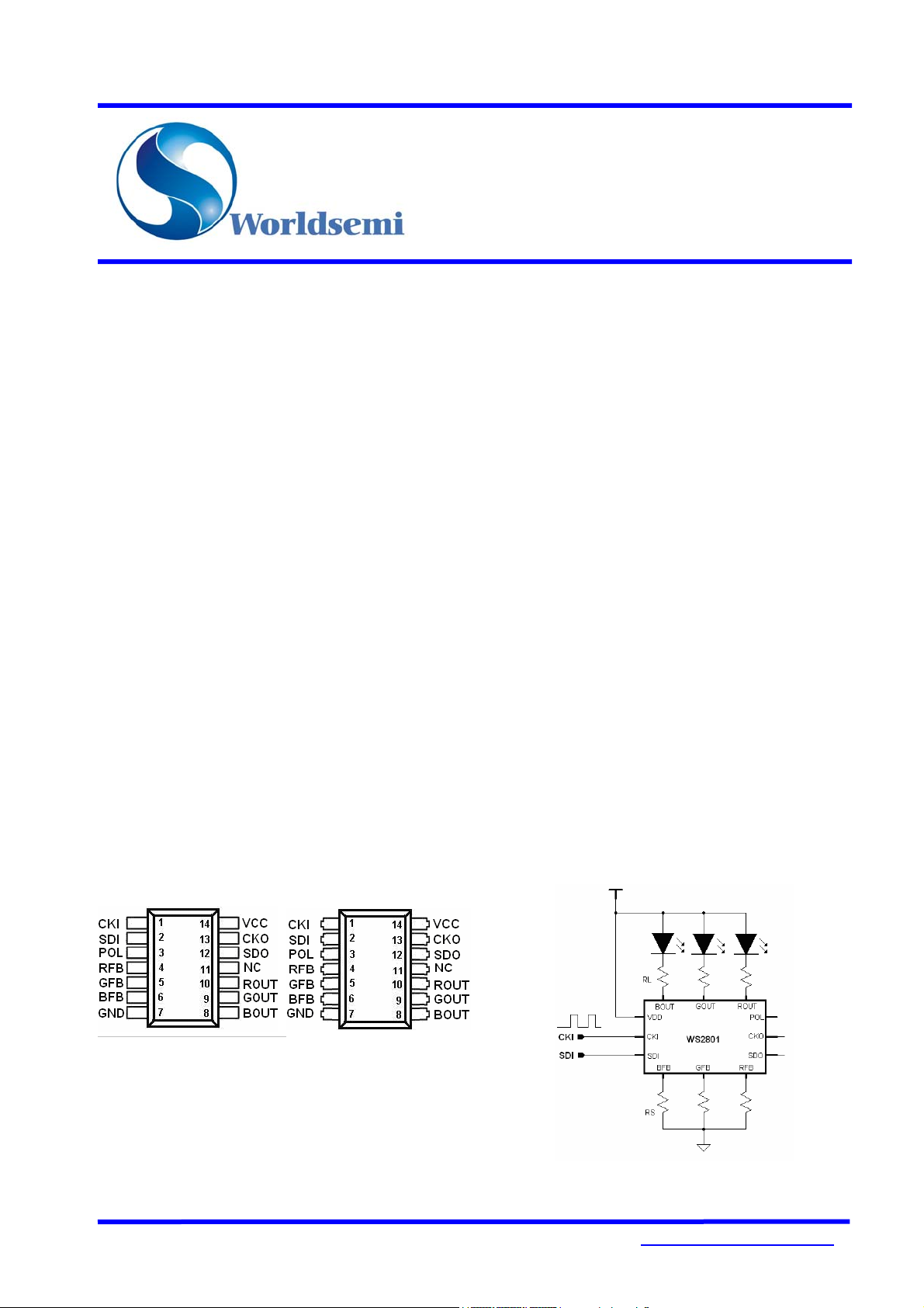
Pin Configurations
• LED decorative lighting
• Indoor/Outdoor LED video or massage display
• PWM signal generator
• LCD TV back lighting
Ty pical Application Circuit
Fig1.a SOP-14 package Fig1.b DIP-14 package
1 /15
WS-Preliminary-V0.3 http://www.world-semi.com
Page 2
Preliminary WS2801
3-Channel Constant Current
LED Driver With Programmable
PWM Outputs
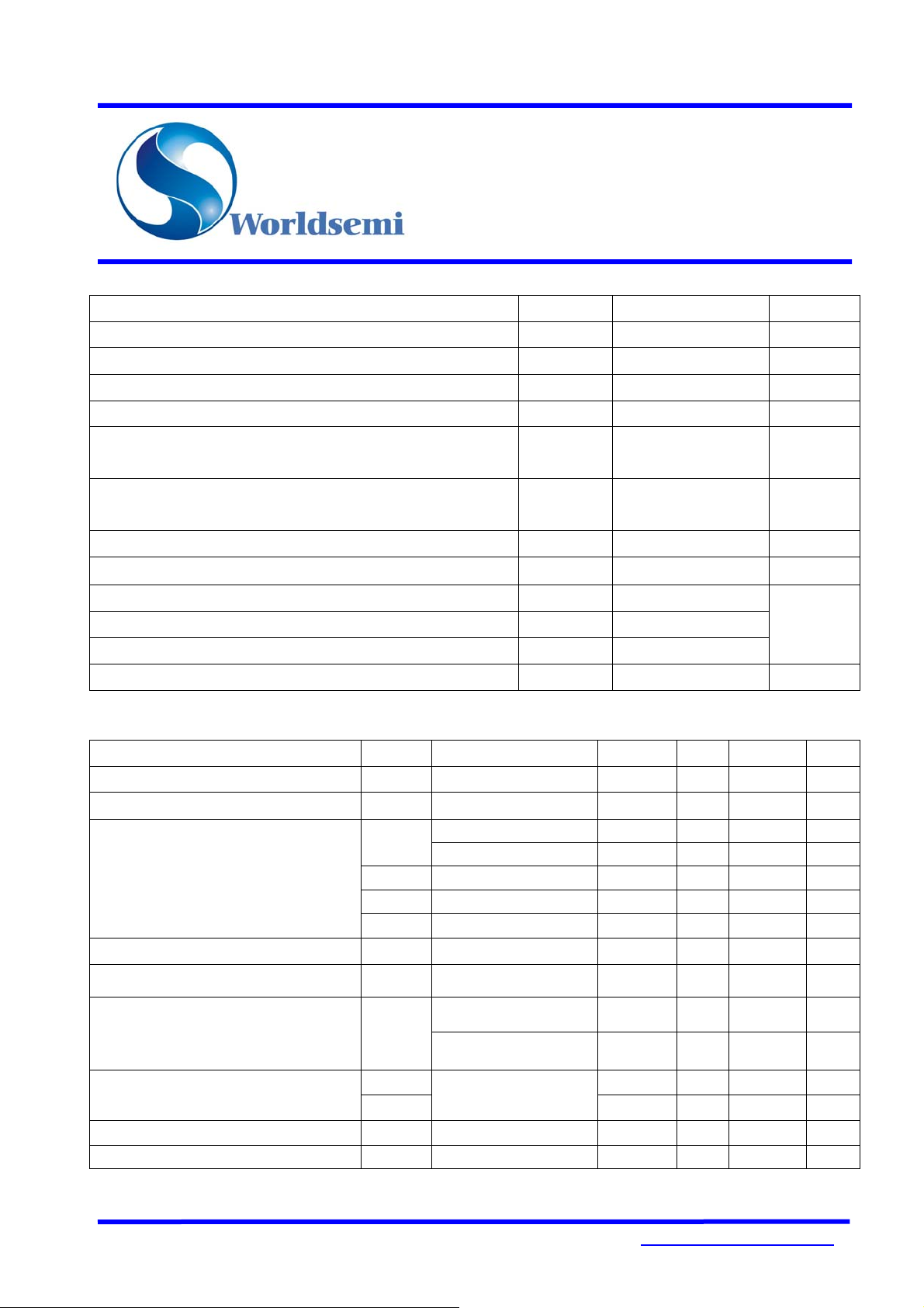
Absolute Maximum Ratings
Parameter Symbol Ratings Unit
Power Supply Voltage VCC -0.3 to 6V V
Input Voltage V
Output Voltage V
Output Pin Voltage V
Output Current
Constant Current Drive Mode
Constant Voltage Drive Mode
Output Current Deviation (Constant Current Driving Mode)
Between output channels
Between chips
Input Clock Frequency F
Maximum Power Dissipation P
OUT
XOUT
I
OUTCC
I
OUTCV
D
D
CLK
IN
IOI
IOE
D
Operating Junction Temperature Topr -40 to + 150
Storage Temperature Range Tstg -55 to + 150
Lead Temperature (Soldering, 10 seconds)
Tsolder 300
ESD susceptibility 4000 V
Note: If the voltage on the pins exceeds the maximum ratings may cause permanent damage to the device.
Electrical Characteristics (VCC=5V, TA= 25℃, unless otherwise specified.)
Parameter Symbol Conditions Min Typ Max Units
Power Supply Voltage Range V
Output Voltage VOUT IOUT=1uA -0.3 -- 7.0 V
I
outH
Output Current
Standby Supply Current
Minimum Constant Current Output Time I
I
outL
I
SOURCE
I
SINK
I
STB
OH
Input Current I
Input Voltage Level
V
V
Constant Current Feed Back Voltage V
Output Saturation Voltage V
XFB
SAT
3.3 -- 5.5 V
CC
Constant Current Output 5 -- 30 mA
Constant Voltage Output -- -- 50 mA
Output Cut Off -- 0.1 1 uA
Other Output -- 1 -- mA
Other Output -- -1 -- mA
B
R/G/BOUT Floating -- 1 1.5 mA
VIN=V
I
OUT
or VIL,
IH
=20mA
PIN:CKI,SDI
=VDD or GND
V
IN
IH
IL
IN
PIN:CKM,POL
=VDD or GND
V
IN
TA=-40~125℃
B R
R/G/BFB
=20Ω B
IOUT=20mA -- 0.4 0.6 V
-0.3 to VCC+0.3V V
-0.4 to 7V V
-0.3 to 7V V
0 to 50
mA
0 to 100
±1
%
±3
25 MHz
600 mW
℃
-- 14 -- uS
-- --
--
±10 ±20
±1
uA
uA
0.8*VDD -- VDD V
GND -- 0.2*VDD
0.582 0.6 0.618
V
V
2 /15
WS-Preliminary-V0.3 http://www.world-semi.com
Page 3
Preliminary WS2801
3-Channel Constant Current
LED Driver With Programmable
PWM Outputs
Output Voltage Regulation %dV
Line Regulation %dV
Pull High Resistance R
OUTVOUT
CC
INHIGH
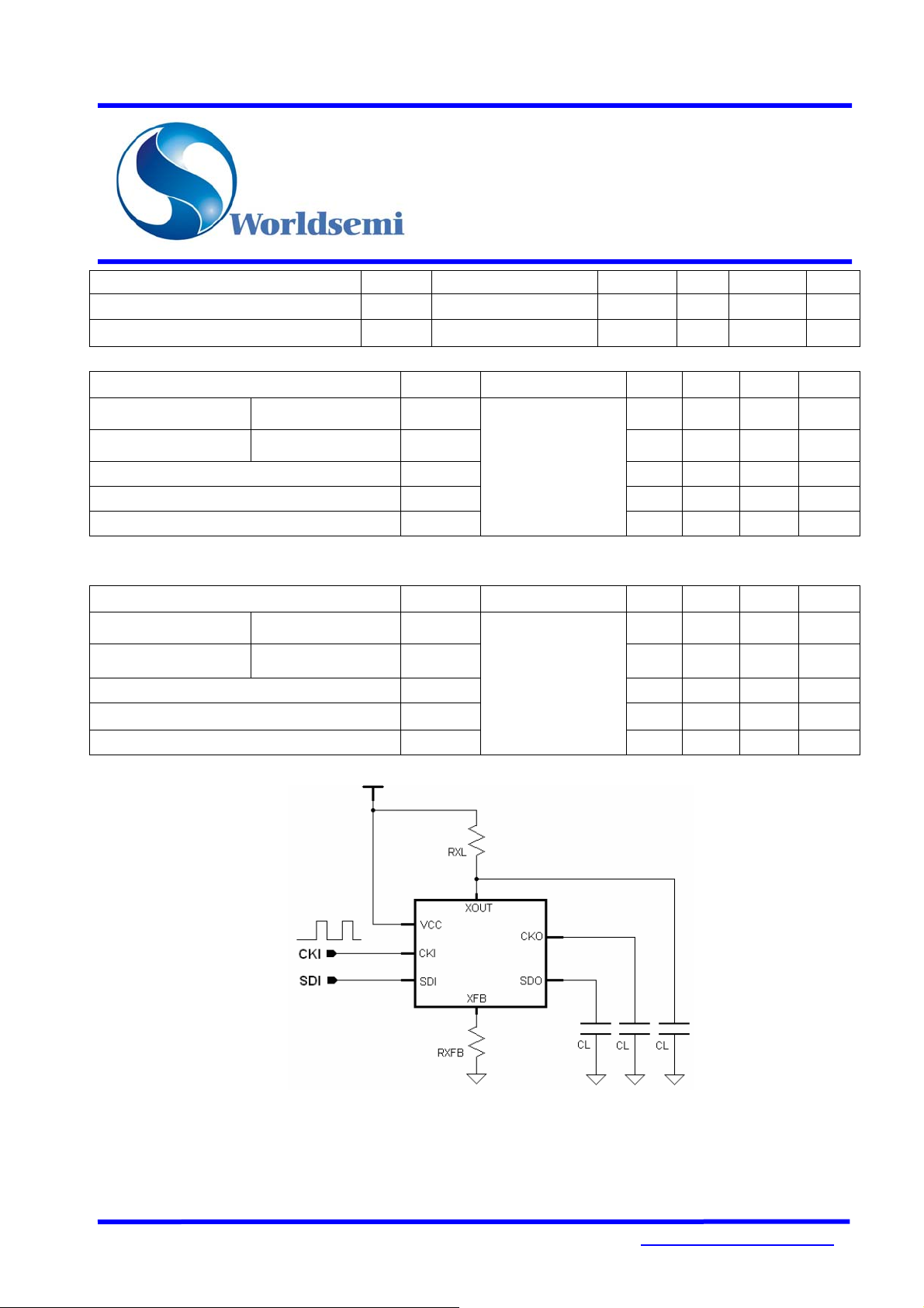
Switching Characteristics (VCC=5V, TA=25℃)
Parameter Symbol Conditions Min Typ Max Units
Propagation Delay
(‘L’ to ‘H’)
Propagation Delay
(‘L’ to ‘H’)
Output Current Rise Time
Maximum Turn ON and OFF time of Drive Current
Output Current Propagation
CKI-to-CKO
CKI-to-CKO
Switching Characteristics (VCC=3.3V, TA=25℃)
Parameter Symbol Conditions Min Typ Max Units
Propagation Delay
(‘L’ to ‘H’)
Propagation Delay
(‘L’ to ‘H’)
Output Current Rise Time
Output Current Fall Time
Output Current Propagation
CKI-to-CKO
CKI-to-CKO T
Circuit for Switching Characteristics Test
=0.9~4, R
VCC=4~5.5V --
R
POL
T
T
①T
T
①T
pLH
pHL
T
or
T
of
OP
pLH
pHL
T
or
T
of
OP
VIH=VCC
V
R
RL=180Ω
CL=30pF
VIH=VCC
V
R
RL=180Ω
CL=30pF
RGBFB
, R
CKM
=GND
IL
XFBs
=GND
IL
XFBs
=30Ω
=30
=30Ω
--
±0.1
±0.1
-- 30 -- KΩ
-- 8 -- ns
-- 8.6 -- ns
-- 50 -- ns
-- 50 -- ns
-- -- 3.3 mS
-- 9.0 -- ns
-- 13 -- ns
-- 50 --
-- 50 -- ns
-- -- 3.3 mS
-- %/V
-- %/V
Fig2, Circuit for switching characteristics test
Note:
① Reload the gray scale data at each end of the PWM cycle
3 /15
WS-Preliminary-V0.3 http://www.world-semi.com
Page 4
Preliminary WS2801
3-Channel Constant Current
LED Driver With Programmable
PWM Outputs
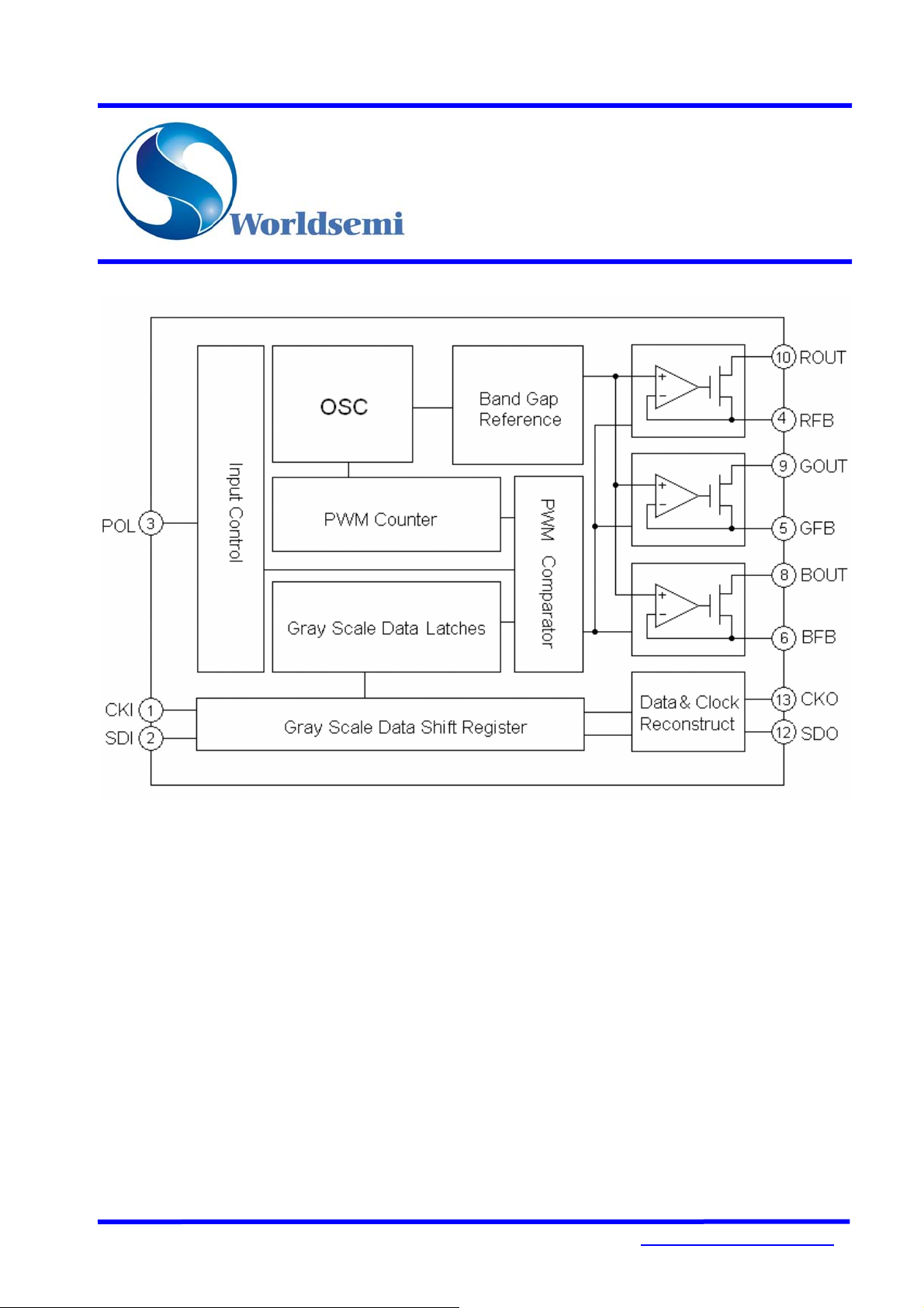
Typical Block Diagram
Fig3, Block Diagram of WS2801
4 /15
WS-Preliminary-V0.3 http://www.world-semi.com
Page 5
Preliminary WS2801
3-Channel Constant Current
LED Driver With Programmable
PWM Outputs
Pin Description
Pin Port Pin Name Pin Description
1
2 SDI Serial gray scale data input
3 POL
4 RFB
5 GFB
6 BFB
7 GND Ground
8 BOUT The output of the B channel
9 GOUT The output of the G channel
10 ROUT The output of the R channel
11 NC None connection
12 SDO The output of the serial gray scale data.
13 CKO The output of the buffered clock
14 VCC
Application Information
CKI Data clock input
Output polarity control. When this pin is pull to GND, the driver output will be
reversed; when floating or pulled high, the output polarity will not be reversed.
The feed back of the R channel, a resistor connected to this pin can set the
output constant current of the R channel
The feed back of the G channel, a resistor connected to this pin can set the
output constant current of the G channel
The feed back of the B channel, a resistor connected to this pin can set the
output constant current of the B channel
Power supply input, a capacitor can be connected from this pin to GND to
enhance the noise immunity.
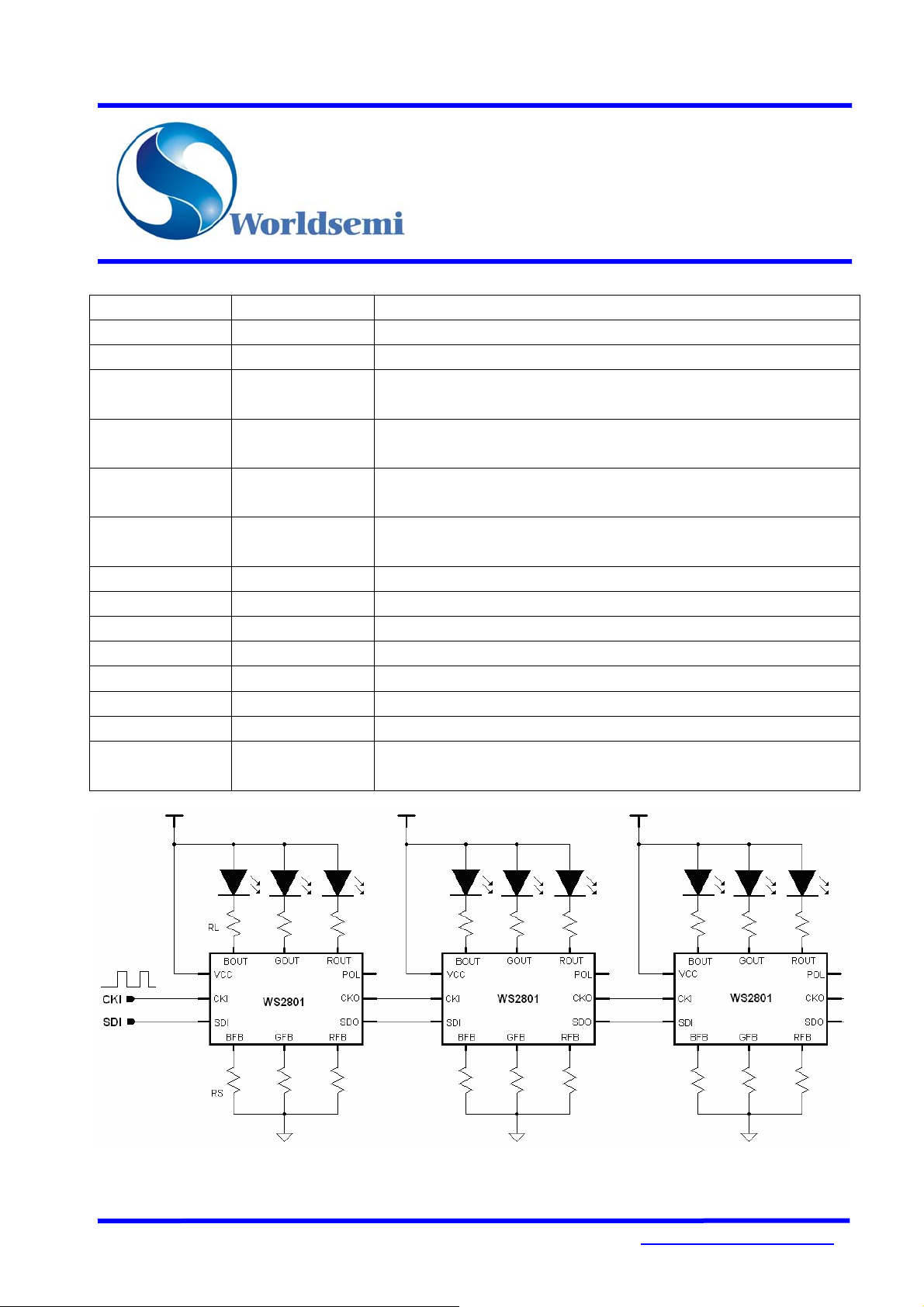
Fig4, The typical application circuit of WS2801
5 /15
WS-Preliminary-V0.3 http://www.world-semi.com
Page 6
Preliminary WS2801
B
3-Channel Constant Current
LED Driver With Programmable
PWM Outputs
Figures
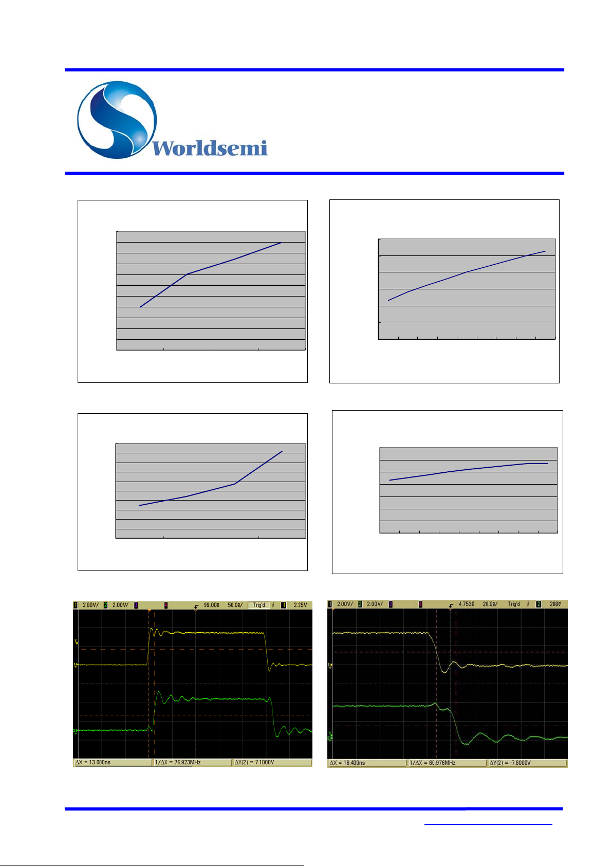
Iout vs. VCC
VFB vs temp
Iout(mA))
30.1
30.05
29.95
29.9
29.85
29.8
29.75
29.7
29.65
29.6
29.55
30
3455.5
VCC(V)
VF
0.63
0.62
0.61
0.6
0.59
0.58
0.57
-40 - 20 0 20 40 60 80 100 120
Output current vs. Temp (RFB=20Ω) Feed back voltage vs. temp.
IVCC vs. Temp.
IOUT(mA)
30.1
30.05
29.95
29.9
29.85
29.8
29.75
29.7
29.65
29.6
IOUT vs.VOUT
1400
30
1200
1000
800
600
IVCC(uA)
400
200
0
2345
VOUT(V)
-40 -20 0 20 40 60 80 100 120
Temp.
Temp.(℃)
Output current vs. output voltage I
vs. Temp.
VCC
6 /15
WS-Preliminary-V0.3 http://www.world-semi.com
Page 7
Preliminary WS2801
3-Channel Constant Current
LED Driver With Programmable
PWM Outputs
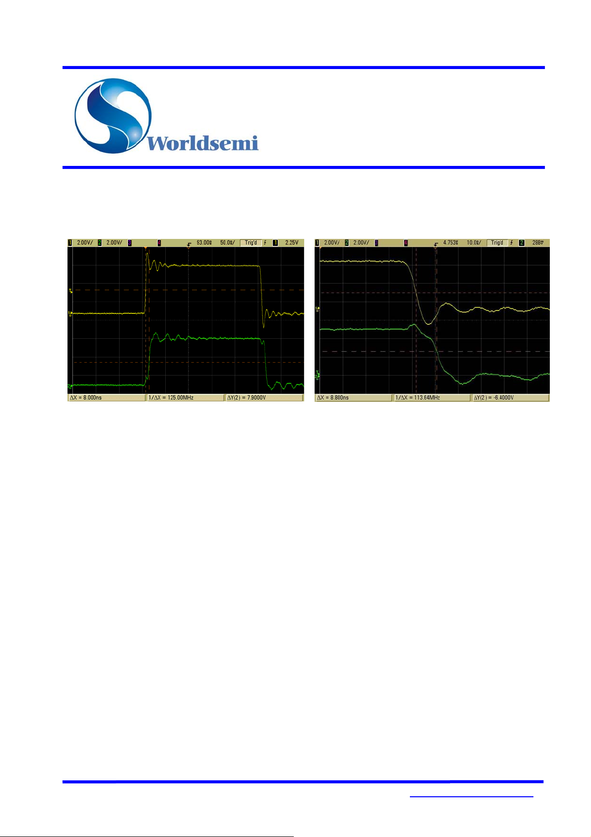
CKI to CKO delay time at rising edge(VCC=3.3V)
Channel1: CKI
Channel2: CKO
CKI to CKO delay time at falling edge(VCC=3.3V)
Channel1: CKI
Channel2: CKO
CKI to CKO delay time at rising edge(VCC=5V)
Channel1: CKI
Channel2: CKO
CKI to CKO delay time at falling edge(VCC=5V)
Channel1: CKI
Channel2: CKO
7 /15
WS-Preliminary-V0.3 http://www.world-semi.com
Page 8
Preliminary WS2801
3-Channel Constant Current
LED Driver With Programmable
PWM Outputs
Application note:
Higher Voltage Applications:
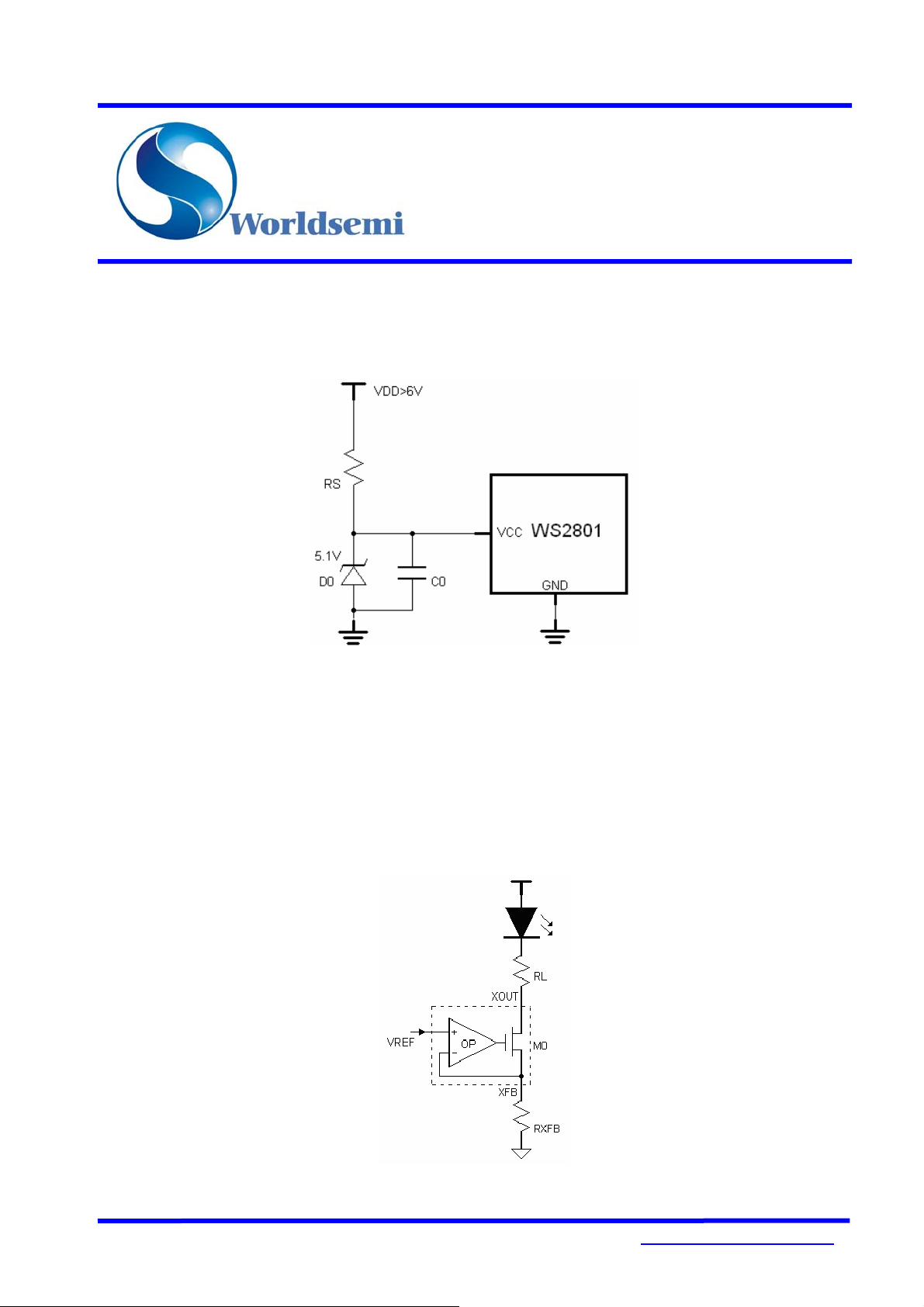
The power supply range of WS2801 is from 3.3 to 6V, when the input power supply voltage is higher than 6V, a zener diode D0
can be used to clamp the voltage to generate the power supply of the chip, see Fig 6.
Fig5, the power supply for high voltage application VDD>6V
As the WS2801 dissipates about 1.5mA current during normal operation, the current limit resistor RS should be about 2 or more
times of the current that dissipated in WS2801, if the power supply VDD=12V, then RS=2KΩ functions well. A capacitor C0 is
necessary to filter the noise on the generated power supply voltage for WS2801, and C0=1uF functions well for most of the
applications.
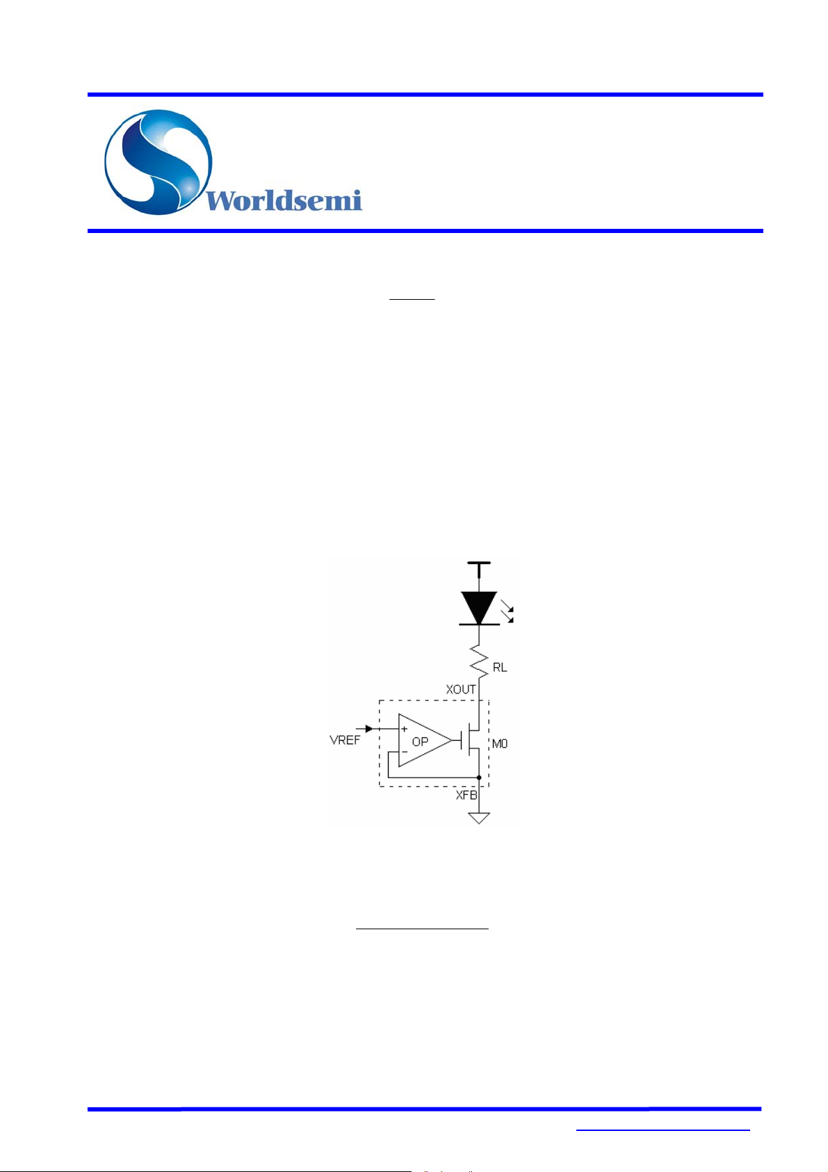
Constant Driving Current Mode
In WS2801, a high performance OpAmp is applied to control the pass element M0 to generate a constant output current to drive
the external LED strings. The output current of each channel can be set by adjusting the current feed back resistor connected at
the current feed back pin(R/G/BFB), see Fig7.
Fig6, The schematic of constant current drive mode
8 /15
WS-Preliminary-V0.3 http://www.world-semi.com
Page 9
Preliminary WS2801
−
−
3-Channel Constant Current
LED Driver With Programmable
PWM Output
The output constant current can be set by the following equation:
V
R
REF
---------------------------------------------------------------------------- (1)
XFB
is the current feed back resistor connected on R/G/BFB pin,
B
XFB
I =
XOUT
Where V
for example RXFB=30Ω to set IXOUT=20mA,则RXFB=30Ω.
To guarantee the normal operation of the constant current drive, the voltage on R/G/BOUT should be set between 1 to 1.5 V, and
then the drive can output a high precision current over whole operation range, meanwhile there would be not too much power
dissipated on WS2801.
Constant Voltage Driving Mode
WS2801 is a versatile LED driver, it does not only provide user constant current driving mode, but also constant voltage driving
mode, which is compatible with ZQL9712. The constant voltage driving mode (POL=’HIGH’ or floating) can drive the LEDs with
current up to 50mA. Connecting R/G/BFB directly to ground, then WS2801 can operate at constant voltage driving mode. See Fig
8.
=0.6V, which is the current setting reference voltage, R
REF
Fig7, The schematic of constant voltage driv ing mode
At constant voltage driving mode, the LED diving current can be set by adjusting RL; the RL can be derived by the following
equation:
VVV
=
R
L
Where RL is the current setting resistor, VDD is the LED power supply, VLED is the LED forward conducting voltage drop, VOUT is
the saturation voltage of the output driver(about 0.2~0.4V), ILED is the LED operating current, usually ILED≤20mA.
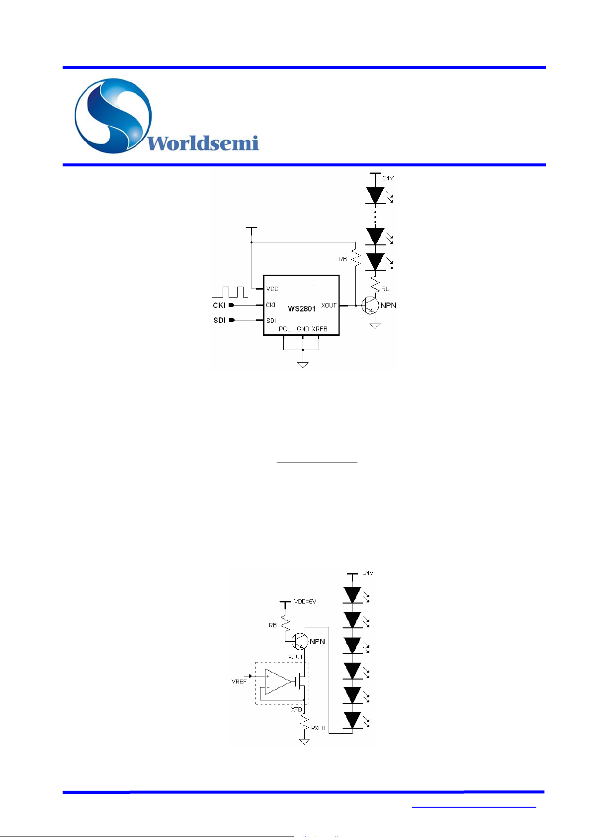
Constant Voltage Driving Mode with External Switches
WS2801 provides constant voltage driving mode with external switches to drive high brightness LED, and also realize the HB LED
256 gray scales control, when POL is pull to GND, WS2801 can operate at this driving mode, see Fig9.
I
LED
OUTLEDDD
---------------------------------------------------------------- (2)
9 / 15
WS-Preliminay-V0.3 http://www.world-semi.com
Page 10
Preliminary WS2801
−
−
3-Channel Constant Current
LED Driver With Programmable
PWM Output
Fig8, Constant Voltage Drivin g with External Power Switches.
This driving mode is mainly used in high input voltage, high LED driving current (ILED>300mA). Its operating principle is using the
external power NPN switches to driving the LED lamps. The LED driving current can be adjusted by the external current limiting
resistor RL, RL can be derived by the following equation:
VVV
CELEDDD
R
=
L
The external NPN transistor operates in saturation region, VCE is the saturation voltage, and VCE=0.5~0.8V, the base resistor
RB=2~5K.
Constant Current Driving Mode with External Switches
This driving mode makes WS2801 can drive the cascading LED lamps with extreme low cost, at this mode, POL=’HIGH’ or
floating, see Fig10.
I
LED
------------------------------------------------------------- (2)
Fig9, Constant current drive with external switches
10 / 15
WS-Preliminay-V0.3 http://www.world-semi.com
Page 11

Preliminary WS2801
−
[
[][][
3-Channel Constant Current
LED Driver With Programmable
PWM Output
This mode can be used to drive the LED strings under high input voltage (VIN>6V), the highest application voltage is determined
by the external NPN power switch. The current flows through the collector of the NPN transistor:
β
The current flow through the base is:
II =
XOUTNPNC
--------------------------------------------------------------- (4)
1β+
1
II =
B
XOUTNPN
β+
During normal operation, to avoid too much power dissipating on WS2801, the voltage at R/G/BOUT should be set around 1.2
volts; the value of RB can be derived by the following equation:
VV
I
XOUTDD
NPNB
=
R
B
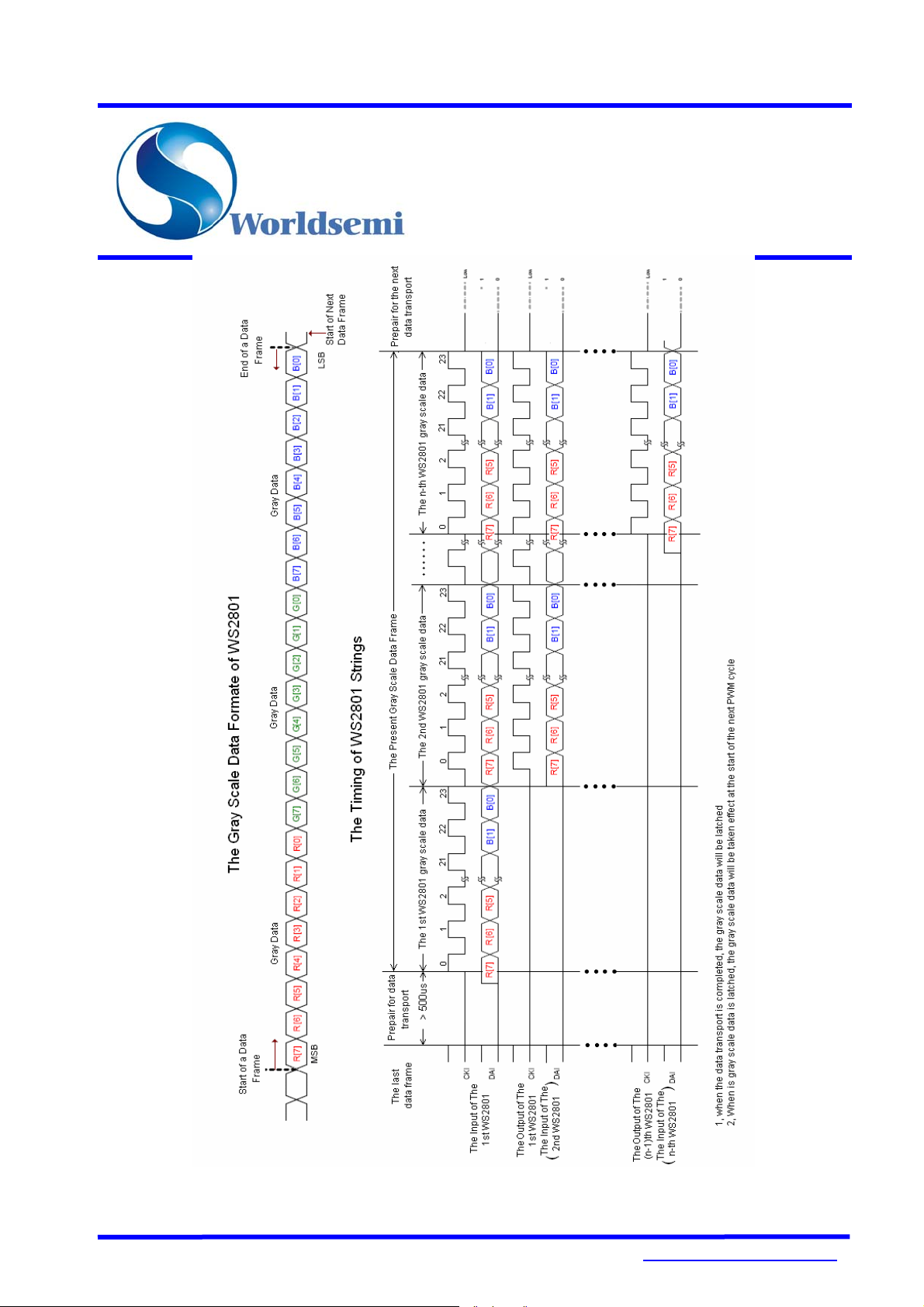
Gray Scale Data Word Format and Timing
CLK pin keeps low more than 500uS will make the WS2801 internal status register reset, and at this moment, the gray scale data
in the data shift registers will be latched. Now WS2801 is ready for gray scale data transport. When the WS2801 receives total 24
clock rising edges, the WS2801 enters relay mode, which relays the input signal got from CKI and SDI with very low distortion
(100pS typical) and very low delay time ( 8 ns typical). The data format and the timing diagram can be seen in Fig 11.
The gray scale data frame is comprised of 3 gray data words, each data word is composed of 8 gray scale data bits, total 24 bits.
The 8bit gray data can easily realize the linear 256 LED gray levels control.
During data transfer, the first bit is the data frame signal, then is the MSB of the ROUT channel, the last one transferred into the
data shift register is the LSB of the BOUT channel.
The duty cycle of the LED driving current can be calculated as:
D
XOUT
Where L[x]=”0” or “1”, which is R、 G 、 B[x], x=0,1,2……7 in the gray scale data. Gray scale data
0000 0000 is for the minimum 0 duty ratio, and 1111 1111 is f o r t h e maxim u m 255/256 duty ratio.
][][]
=
--------------------------------------------------------------- (5)
1
---------------------------------------------------------------------- (6)
][][]
256
1234567
02*12*22*32*42*52*62*7
LLLLLLLL
+++++++
----- (7)
11 / 15
WS-Preliminay-V0.3 http://www.world-semi.com
Page 12
Preliminary WS2801
3-Channel Constant Current
LED Driver With Programmable
PWM Output
Fig 10, WS2801 data format and timing
12 / 15
WS-Preliminay-V0.3 http://www.world-semi.com
Page 13

Preliminary WS2801
3-Channel Constant Current
LED Driver With Programmable
PWM Output
The Connection and Driving of Cascading Operation
The transmit the data over long distance by cascading, the WS2801 integrates push-pull output stage with strong driving
capability which enables the data and clock can be transmitted up to 6 meters at 2MHz clock frequency.
To prevent the reflection, it is necessary to connect a 50Ω resistor at the data input or output port for impedance match.
13 / 15
WS-Preliminay-V0.3 http://www.world-semi.com
Page 14
Preliminary WS2801
3-Channel Constant Current
LED Driver With Programmable
PWM Output
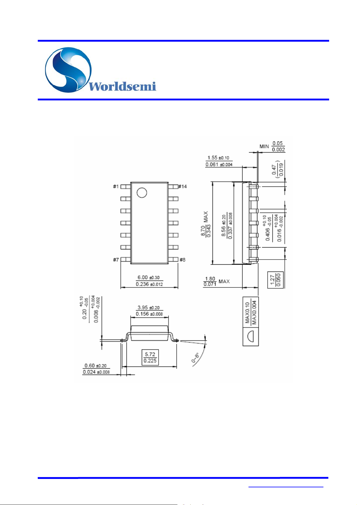
Package Information
SOP-14 Package (Unit: mm)
14 / 15
WS-Preliminay-V0.3 http://www.world-semi.com
Page 15
Preliminary WS2801
3-Channel Constant Current
LED Driver With Programmable
PWM Output
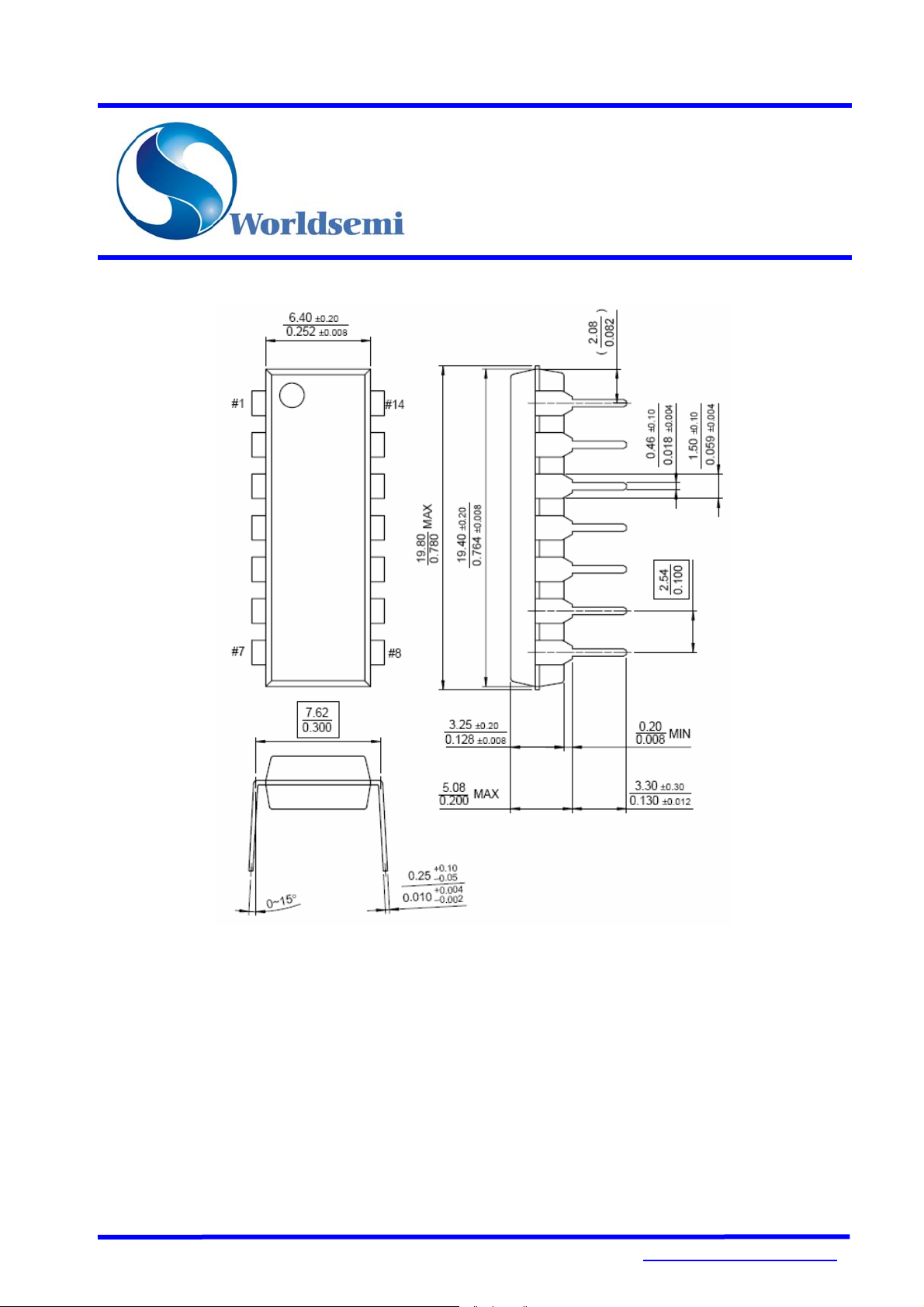
DIP-14 Package (Unit: mm)
IMPORTANT NOTICE
The information in this document has been carefully reviewed and is believed to be accurate.
Nonetheless, this document is subject to change without notice. World-Semi assumes no responsibility
for any inaccuracies that may be contained in this document, and makes no commitment to update or to
keep current the contained information, or to notify a person or organization of any update. World-semi
reserves the right to make changes, at any time, in order to improve reliability, function or design and to
attempt to supply the best product possible.
World Semiconductor, Inc
Nov. 2008
15 / 15
WS-Preliminay-V0.3 http://www.world-semi.com
Page 16

 Loading...