DESCRIPTION
The KH Series is ideally suited for volume use
in OEM applications such as remote control and
command, and keyless entry. Housed in a
compact SMD package, it combines a highlyoptimized RF transmitter with an on-board
encoder. When paired with a matching KH
Series receiver / decoder module, a reliable
wireless link is formed, capable of transferring
the status of 8 parallel inputs over distances in
excess of 300 feet. Ten tri-state address lines
provide 59,049 (3
10
) addresses for security and
uniqueness. No external RF components are
required (except an antenna), making
integration straightforward.
KH SERIES TRANSMITTER / ENCODER DATA GUIDE
WIRELESS MADE SIMPLE
®
Revised 10/12/06
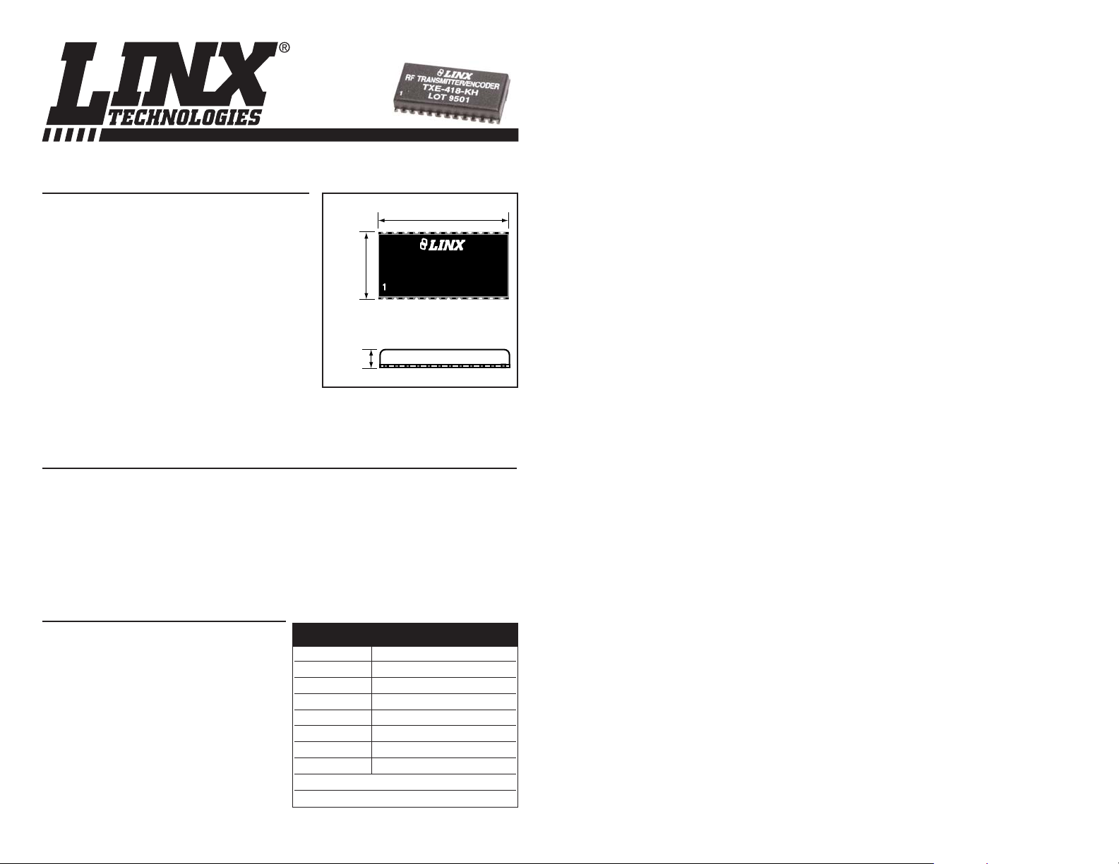
Figure 1: Package Dimensions
Remote Control / Command
Keyless Entry
Garage / Gate Openers
Lighting Control
Call Systems
Home / Industrial Automation
Fire / Security Alarms
Remote Status Monitoring
Wire Elimination
APPLICATIONS INCLUDE
Low cost
On-board encoder
8 parallel binary inputs
3
10
addresses for security and
uniqueness
No external RF components
required
Ultra-low power consumption
Compact SMD package
Stable SAW-based architecture
Adjustable output power
Transmit enable line
No production tuning
FEATURES
PART # DESCRIPTION
TXE-315-KH Transmitter 315MHz
TXE-418-KH Transmitter 418MHz
TXE-433-KH Transmitter 433MHz
RXD-315-KH Receiver 315MHz
RXD-418-KH Receiver 418MHz
RXD-433-KH Receiver 433MHz
EVAL-***-KH Basic Evaluation Kit
*** = 315, 418 (Standard), 433.92MHz.
Transmitters are supplied in tubes of 20 pcs.
ORDERING INFORMATION
TXE-315-KH
TXE-418-KH
TXE-433-KH
0.630"
RF TRANSMITTER/ENCODER
0.180"
1.220"
TXE-418-KH
LOT 2000

Page 3
Page 2
ELECTRICAL SPECIFICATIONS
*CAUTION*
This product incorporates numerous static-sensitive components.
Always wear an ESD wrist strap and observe proper ESD handling
procedures when working with this device. Failure to observe this
precaution may result in module damage or failure.
1. Current draw with 50% mark / space ratio.
2. Into a 50Ω load.
3. With 430Ω resistor on LADJ.
4. Characterized, but not tested.
Notes
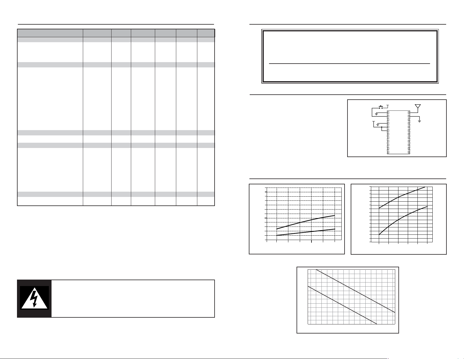
Table 1: KH Series Transmitter Electrical Specifications
Parameter Designation Min. Typical Max. Units Notes
POWER SUPPLY
Operating Voltage V
CC
2.7 – 5.2 VDC –
Supply Current I
CC
– 1.5 – mA 1,4
Power-Down Current I
PDN
– 1.0 – µA –
TRANSMITTER SECTION
Transmit Frequency Range: F
C
TXE-315-KH – 315 – MHz –
TXE-418-KH – 418 – MHz –
TXE-433-KH – 433.92 – MHz –
Center Frequency Accuracy – -75 – +75 kHz –
Output Power P
O
-4 +2 +4 dBm 2,3
Harmonic Emissions: P
H
TXE-315-KH -40 – – dBc –
TXE-418-KH -40 – – dBc –
TXE-433-KH -45 – – dBc –
ANTENNA PORT
RF Output Impedance R
OUT
–50–Ω 4
ENCODER SECTION
Data Length – – 26 bits 3x – – –
Average Data Duty Cycle – – 50% – – 4
Encoder Oscillator F
ENC
– 70 – kHz 4
Data Input:
Logic Low – 0.0 – 0.2 x V
CC
VDC 4
Logic High V
CC
x 0.8 – V
CC
VDC 4
Input Sink Current – 0.6 1.0 1.2 mA 4
ENVIRONMENTAL
Operating Temperature Range – -30 – +70
°C4
ABSOLUTE MAXIMUM RATINGS
Supply Voltage V
CC
-0.3 to +6.0 VDC
Any Input or Output Pin -0.3 to V
CC
VDC
Operating Temperature -30 to +70 °C
Storage Temperature -45 to +85 °C
Soldering Temperature +225°C for 10 seconds
*NOTE* Exceeding any of the limits of this section may lead to permanent
damage to the device. Furthermore, extended operation at these maximum
ratings may reduce the life of this device.
PERFORMANCE DATA
These performance parameters
are based on module operation at
25°C from a 3.0VDC supply unless
otherwise noted. Figure 2
illustrates the connections
necessary for testing and
operation. It is recommended all
ground pins be connected to the
ground plane.
Figure 2: Test / Basic Application Circuit
TYPICAL PERFORMANCE GRAPHS
Figure 3: Supply Current vs. Supply Voltage Figure 4: Output Power vs. Supply Voltage
Figure 5: Output Power vs. LADJ Resistor
3VDC
VCC
ANT
GND
24
23
A9
22
A8
21
A7
20
A6
19
A5
18
A4
17
A3
16
A2
15
A1
14
A0
13
1
GND/LVL
2
D0
D1
3
4
GND
5
VCC
6
TE
D2
7
8
D3
D4
9
D5
10
D6
11
D7
12
12
11
10
9
8
7
6
5
4
3
2
Supply Current (mA)
1
0
With LADJ tied to ground
With 430Ω resistor on LADJ
2.5
3.0
3.5
4.0 4.5
5.0
Supply Voltage (V)
+8
With LADJ tied to ground
+7
+6
+5
+4
+3
+2
+1
0
-1
-2
-3
-4
-5
-6
Output Power Into 50 ohms (dBm)
-7
With 430Ω resistor on LADJ
2.5
3.0
3.5
Supply Voltage (V)
4.0 4.5
5.0
+8
+7
+6
+5
+4
+3
+2
+1
0
-1
Output Power (dBm)
-2
-3
-4
51 100 150 200 240 300 360 430 510 560 620 680 750 820 910 1.1K
5V
3V
LADJ Pin Resistor Value (Ω)

Page 5Page 4
PIN ASSIGNMENTS
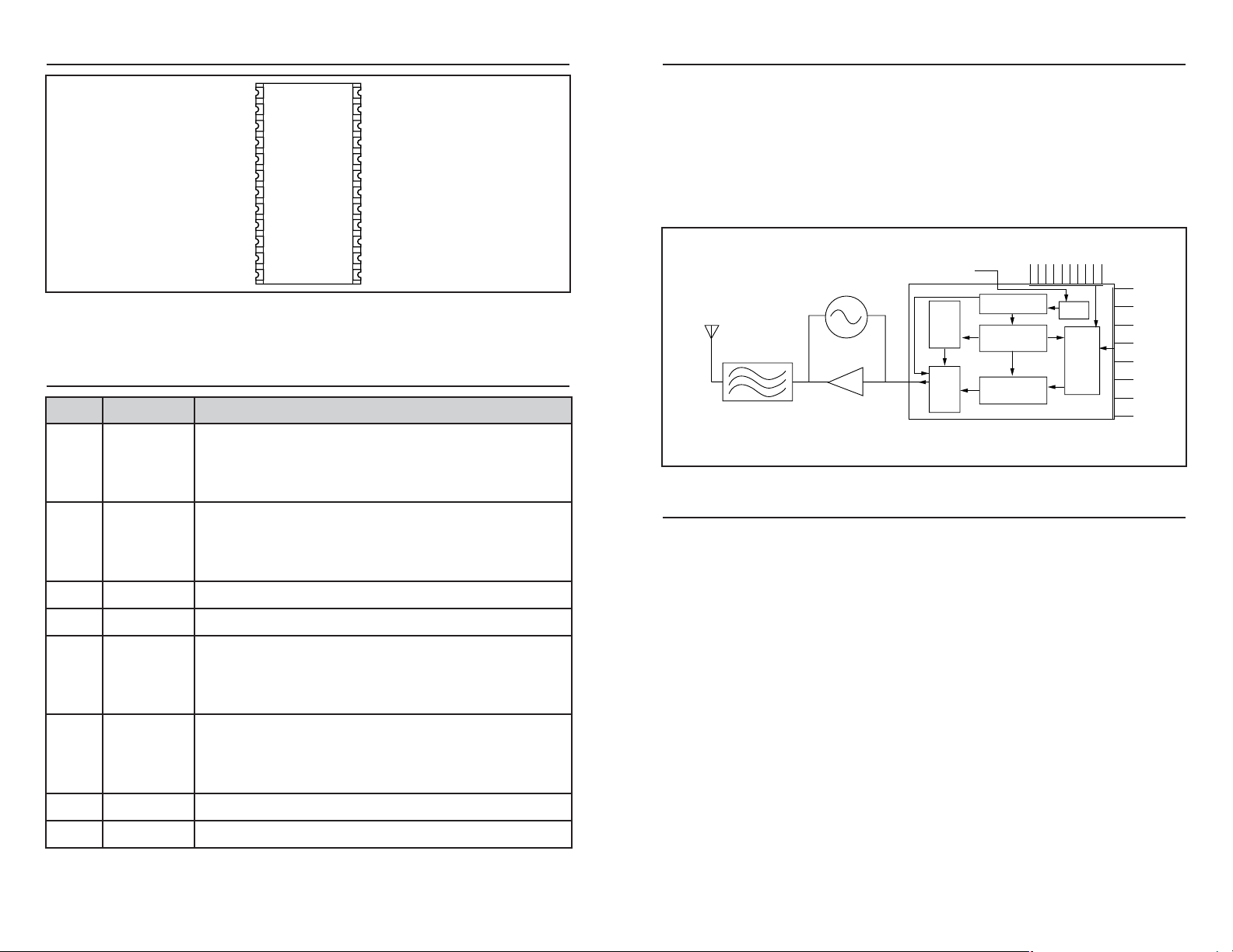
Figure 6: KH Series Transmitter Pinout (Top View)
Pin # Name Description
1 GND / LADJ
Level Adjust. This line can be used to adjust the output
power level of the transmitter. Connecting to GND will give
the highest output, while placing a resistor to GND will
lower the output level.
2, 3,
7-12
D0 - D1
Data Input Lines. When TE goes high, the module will
encode the state of these lines for transmission. Upon
receipt of a valid transmission, the receiver / decoder will
replicate these lines on its output lines.
4 GND Analog Ground
5
V
CC
Supply Voltage
6 TE
Transmit Enable Line. When this line goes high, the
module will encode the states of the address and data lines
into a packet and transmit the packet three times.
13-22 A0-A9
Address Lines. The state of these lines must match the
state of the receiver’s address lines in order for a
transmission to be accepted.
23 GND Analog Ground
24 ANT 50-ohm RF Output
PIN DESCRIPTIONS
MODULE DESCRIPTION
The KH Series transmitter / encoder module combines a high-performance
Surface Acoustic Wave (SAW) based transmitter with an on-board encoder.
When combined with a Linx KH Series receiver / decoder, a highly reliable RF
link capable of transferring control or command data over line-of-sight distances
in excess of 300 feet is formed. The module accepts up to 8 parallel inputs, such
as switches or contact closures, and provides ten tri-state address lines for
security and creation of 59,049 (310) unique transmitter / receiver relationships.
The KH’s compact surface-mount package integrates easily into existing designs
and is friendly to hand production or automated assembly.
THEORY OF OPERATION
The KH Series transmitter operation is straightforward. When the Transmit
Enable (TE) line is taken high, the on-board encoder IC is activated. The encoder
detects the logic states of the data and address lines. These states are formatted
into a 3-word transmission, which continues until the TE line is taken low. The
encoder creates a serial data packet that is used to modulate the transmitter.
The transmitter section is based on a simple, but highly-optimized, architecture
that achieves a high fundamental output power with low harmonic content. This
ensures that most approval standards can be met without external filter
components. The KH Series transmitter is exceptionally stable over variations in
time, temperature, and physical shock as a result of the precision SAW device
that is incorporated as the frequency reference.
The transmitted signal may be received by any Linx KH Series receiver / decoder
module or Linx LC or LR Series receiver combined with the appropriate decoder
IC. Once data is received, it is decoded using a decoder IC or custom
microcontroller. The transmitted address bits are checked against the address
settings of the receiving device. If a match is confirmed, the decoder’s outputs
are set to replicate the transmitter’s inputs.
Figure 7: KH Series Transmitter Block Diagram
LADJ/GND
1
D0
2
D1 A9
3
GND
4
VCC
5
TE
6
D2
7
817
D3
9
D4
10
D5
11
D6 A1
12 13
ANT
GND
A8
A7
A6
A5
A4
A3
A2
A0D7
24
23
22
21
20
19
18
16
15
14
Address Inputs
A0-A9
OSC
50Ω RF OUT
(ANT)
Keyed Output
SAW
Oscillator
TX Enable
Sync
Divider
Counter
Parallel
Inputs
D0-D7
GATE
TRI-Detect
Output Isolation
& Filter
RF Amplifier
Buffer
RF STAGE ENCODER STAGE

Page 7Page 6
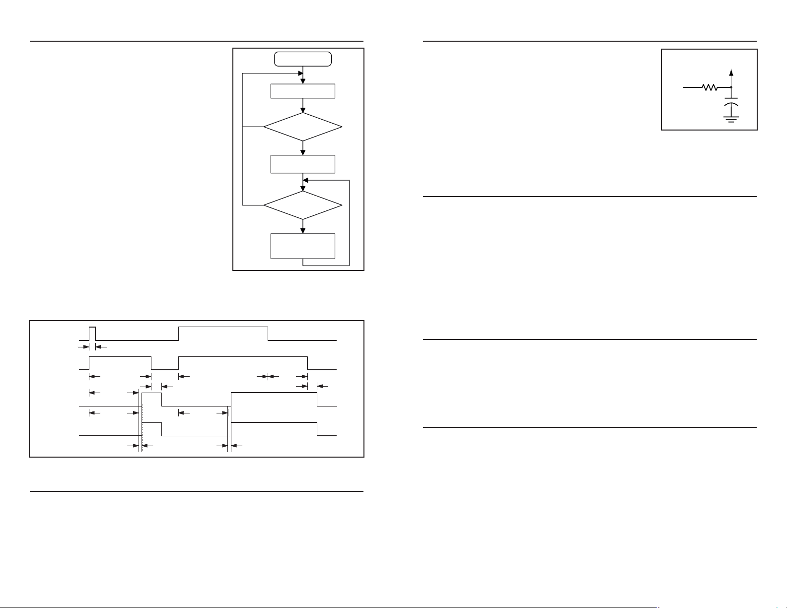
POWER SUPPLY REQUIREMENTS
The module does not have an internal voltage
regulator; therefore it requires a clean, well-regulated
power source. While it is preferable to power the unit
from a battery, it can also be operated from a power
supply as long as noise is less than 20mV. Power
supply noise can affect the transmitter modulation;
therefore, providing a clean power supply for the
module should be a high priority during design.
A 10Ω resistor in series with the supply followed by a
10µF tantalum capacitor from VCCto ground will help in cases where the quality
of supply power is poor. These values may need to be adjusted depending on
the noise present on the supply line.
DATA INPUTS
When the Transmit Enable (TE) line goes high, the states of the eight data input
lines are recorded and encoded for transmission. The data lines are tri-state,
which means that they can be high, low, or floating, though the decoder will
interpret the floating state as a low. This feature means that the data lines do not
require pull-up or pull-down resistors. The states of the data lines can be set by
switches, jumpers, microcontrollers, or hardwired on the PCB.
The encoder will send the states of the address and data lines three times. If the
TE line is still high, it will begin the cycle again. This means that the states of the
data lines are refreshed with each cycle, so the data lines can be changed
without having to pull TE low. There can be up to a 150mS lag in response as
the transmitter finishes one cycle then refreshes and starts over.
ENABLING TRANSMISSION
The module’s Transmit Enable (TE) line controls transmission status. When
taken high, the module initiates transmission, which continues until the line is
pulled low or power to the module is removed. In some cases this line will be
wired permanently to V
CC
and transmission controlled by switching VCCto the
module. This is particularly useful in applications where the module powers up
and sends a transmission only when a button is pressed on the remote.
USING LADJ
The LADJ line allows the transmitter’s output power to be easily adjusted for
range control, lower power consumption, or to meet legal requirements. This is
done by placing a resistor between GND and LADJ. When LADJ is connected
directly to GND, the output power will be at its maximum. Placing a resistor will
lower the output power by up to 7dB, as shown on Page 3 of this data guide.
This is very useful during FCC testing to compensate for antenna gain or other
product-specific issues that may cause the output power to exceed legal limits.
A variable resistor can be used so that the test lab can precicely adjust the output
power to the maximun level allowed by law. The resistor’s value can be noted
and a fixed resistor substituted for final testing. Even in designs where
attenuation is not anticipated, it is a good idea to place a resistor pad connected
to LADJ and GND so that it can be used if needed.
Figure 10: Supply Filter
ENCODER OPERATION
The KH Series transmitter internally utilizes
the HT640 encoder from Holtek. The
encoder begins a three-word transmission
cycle when the Transmission Enable line
(TE) is pulled high. This cycle will repeat
itself for as long as the TE line is held high.
Once TE falls low, the encoder output
completes its final cycle and then stops as
shown in the Encoder / Decoder Timing
diagram. When a transmission enable signal
is applied, the encoder scans and transmits
the status of the 10 bits of the address code
and the 8 bits of the data serially in the order
A0 to A9, D0 to D7.
The status of each address / data pin can be
individually preset to logic high, low, or
floating. The floating state on the data input
is interpreted as logic low by the decoders
since the decoder output only has two
states. The address pins are usually set to
transmit particular security codes by DIP
switches or PCB wiring, while the data is
selected using push buttons or electronic
switches. The floating state allows the KH transmitter to be used without pull-up
or pull-down resistors on the data and address input lines.
SETTING THE TRANSMITTER ADDRESS
The module provides ten tri-state address lines. This allows for the formation of
up to 59,049 (3
10
) unique transmitter-receiver relationships. Tri-state means that
the address lines have three distinct states: high, low, or floating. These pins
may be hardwired or configured via a microprocessor, DIP switch, or jumpers.
The receiver’s address line states must match the transmitter’s exactly for a
transmission to be recognized. If the transmitted address does not match the
receiver’s local address, then the receiver will take no action.
Figure 8: Encoder Flowchart
Check
Check
< 1 Word
3 Words
Transmitted Continuously
3 Words
1/2 Clock Time
Decoder
Data Out
Decoder VT
Encoder
Data Out
Encoder
Transmit
Enable
1/2 Clock Time
2 Words
214 Clocks
214 Clocks
Figure 9: Encoder / Decoder Timing Diagram
No
No
Power On
Standby Mode
Transmission
Enabled?
Yes
3 Data Words
Transmitted
Transmission
Still Enabled?
Yes
3 Data Words
Transmitted
Continuously
Vcc IN
10Ω
Vcc TO
MODULE
+
10μF
 Loading...