

WJ Company FP2189-PCB900S, FP2189-PCB2140S, FP2189-PCB1900S, FP2189 Datasheet

n
b
t
t
y
f
f
r
FP2189
1 Watt HFET
Product Features
• 50 – 4000 MHz
• Up to +31 dBm P1dB
• Up to +45 dBm Output IP3
• High Drain Efficiency
• 19 dB Gain @ 900 MHz
• MTBF >100 Years
• SOT-89 SMT Package
The Communications Edge TM
Preliminary Product Information
Product Description
The FP2189 is a high performance 1-Watt HFET
(Heterostructure FET) in a low-cost SOT-89 surfacemount package. This device works optimally at a drai
ias of +8 V and 250 mA to achieve +45 dBm outpu
IP3 performance and an output power of +31 dBm a
1-dB compression.
The device conforms to WJ Communications’ long
history of producing high reliability and qualit
components. The FP2189 has an associated MTBF o
greater than 100 years at a mounting temperature o
85°C. All devices are 100% RF & DC tested.
The product is targeted for use as driver amplifiers fo
wireless infrastructure where high performance and high
efficiency are required.
Functional Diagram
4
2
1 3
Function Pin No.
Input 1
Ground 2
Output/Bias 3
Ground 4
Specifications
DC Electrical Parameter Units Min Typ Max
Saturated Drain Current1, I
Transconductance, Gm mS
Pinch Off Voltage2, Vp V
mA 500
dss
350
-2.0
Parameters3 Units Min Typ Max
Frequency Range MHz 50 4000
Small Signal Gain, Gss dB
Output P1dB dBm
Output IP34 dBm
Thermal Resistance °C/W
1. I
is measured with Vgs = 0 V, Vds = 3 V.
dss
2. Pinch-off voltage is measured when Ids = 0.4 mA.
3. Test conditions unless otherwise noted: T = 25ºC, VDS = 8 V, IDQ = 250 mA, frequency = 900 MHz
in an application circuit with ZL = Z
4. 3OIP measured with two tones at an output power of +15 dBm/tone separated by 1 MHz. The
suppression on the largest IM3 product is used to calculate the 3OIP using a 2:1 rule.
LOPT
, ZS = Z
SOPT
.
15
+31
+45
30
Absolute Maximum Ratings
Parameters Rating
Operating Case Temperature
Storage Temperature
Maximum DC Power 4.0 W
RF Input Power (continuous) +20 dBm
Operation of this device above any of there parameters may cause permanent damage
-40 to +85 °C
-40 to +125 °C
Typical Parameters5
Parameter Units Typical
Frequency MHz 915 1960 2140
S21 dB
S11 dB
S22 dB
Output P1dB dBm
Output IP3 dBm
Noise Figure dB
Vdd V
6
I
mA
dq
Idd at P1dB mA
5. Typical parameters represent performance in an application circuit.
6. Idq is the quiescent drain current at small signal output levels. The
current may increase as the output power is increased near its
compression point.
19.1 15.2 13.8
-17 -16 -23
-10 -8 -9
+30.3 +30.8 +31.4
+44.3 +44.2 +45.5
4.2 3.5 4.5
+8 +8 +8
250 250 250
260 330 320
Ordering Information
Part No. Description
FP2189
FP2189-PCB900S 900 MHz Application Circuit
FP2189-PCB1900S 1900 MHz Application Circuit
FP2189-PCB2140S 2140 MHz Application Circuit
1-Watt HFET
(Available in Tape & Reel)
This document contains information on a new product.
WJ Communications, Inc • Phone 1-800-WJ1-4401 • FAX: 408-577-6620 • e-mail: sales@wj.com
Specifications and information are subject to change without notice
• Web site: www.wj.com
May 2002
FP2189
1 Watt HFET
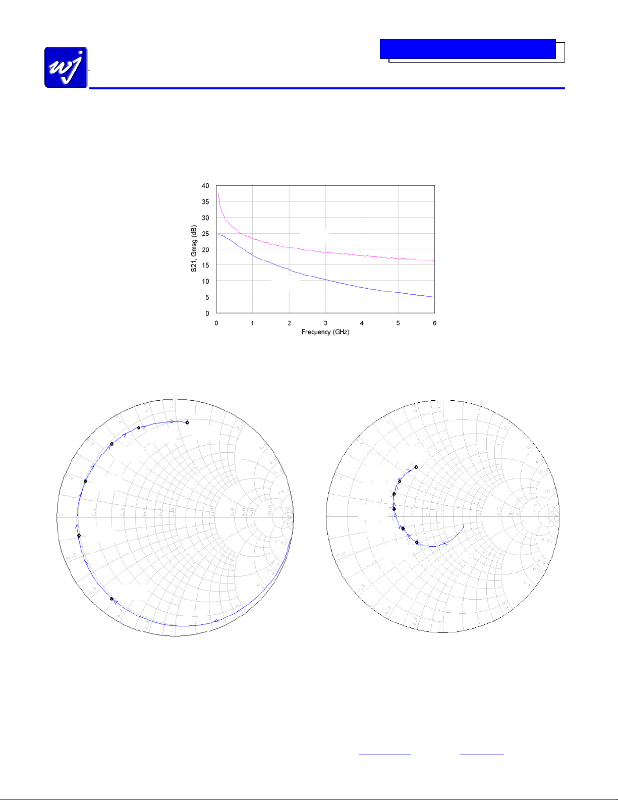
Typical Performance Data
S-Parameters (V
3 GHz
2 GHz
Note:
Measurements were made on the packaged device in a test fixture with 50 ohm input and output lines. The S-parameters
that are shown are the de-embedded data down to the device leads and represents typical performance of the device.
= 8 V, Ids = 250 mA, 25°C, Unmatched 50 ohm system)
ds
S11 vs Frequency
6 GHz
4 GHz
1 GHz
5 GHz
The Communications Edge TM
Preliminary Product Information
Gain, Maximum Stable Gain vs Frequency
G
msg
S21
S22 vs Frequency
6 GHz
5 GHz
4 GHz
3 GHz
2 GHz
1 GHz
This document contains information on a new product.
WJ Communications, Inc • Phone 1-800-WJ1-4401 • FAX: 408-577-6620 • e-mail: sales@wj.com
Specifications and information are subject to change without notice
• Web site: www.wj.com
May 2002
 Loading...