

WJ Company FP1189-PCB-900, FP1189-PCB-1900, FP1189 Datasheet
This document contains information on a new product.
Specifications and information are subject to change without notice
WJ Communications, Inc • Phone 1-800-WJ1-4401 • FAX: 408-577-6620 • e-mail: sales@wj.com
• Web site: www.wj.com
March 2002
The Communications Edge TM
Preliminary Product Information
FP1189
½ Watt HFET
Product Features
• DC – 4000 MHz
• +28 dBm P1dB
• +40 dBm Output IP3
• High Drain Efficiency
• 17 dB Gain @ 1900 MHz
• MTBF >100 Years
• SOT-89 SMT Package
Product Description
The FP1189 is a high performance ½-Watt HFET
(Heterostructure FET) in a low-cost SOT-89 surfacemount package. This device works optimally at a drai
n
b
ias of +8 V and 100 mA to achieve +40 dBm outpu
t
IP3 performance and an output power of +28 dBm a
t
1-dB compression.
The device conforms to WJ Communications’ long
history of producing high reliability and qualit
y
components. The FP1189 has an associated MTBF o
f
over 100 years at a mounting temperature of 85° C. All
devices are 100% RF & DC tested.
The product is targeted for use as driver amplifiers fo
r
wireless infrastructure where high performance and high
efficiency is required.
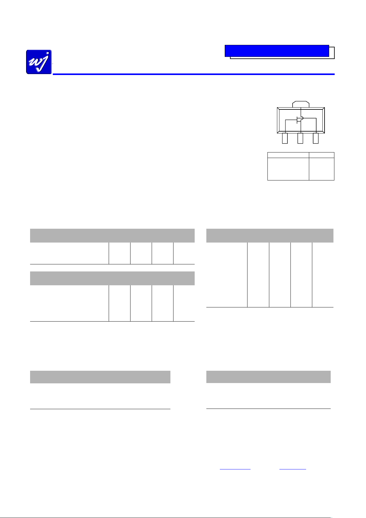
Functional Diagram
1 3
2
4
Function Pin No.
Input 1
Ground 2
Output/Bias 3
Ground 4
Specifications
DC Electrical Parameter Units Min Typ Max
Saturated Drain Current1, I
dss
mA 300
Transconductance, Gm mS
175
Pinch Off Voltage2, Vp V
-2.0
Parameters3 Units Min Typ Max
Frequency Range MHz DC 4000
Small Signal Gain, Gss dB
17
Output P1dB dBm
+28
Output IP34 dBm
+40
Thermal Resistance °C/W
70
1. I
dss
is measured with Vgs = 0 V, Vds = 3 V.
2. Pinch-off voltage is measured when Ids = 0.8 mA.
3. Test conditions unless otherwise noted: T = 25ºC, VDS = 8 V, IDQ = 100 mA, frequency = 1960 MHz
in an application circuit with ZL = Z
LOPT
, ZS = Z
SOPT
.
4. 3OIP measured with two tones at an output power of +15 dBm/tone separated by 1 MHz. The
suppression on the largest IM3 product is used to calculate the 3OIP using a 2:1 rule.
Absolute Maximum Ratings
Parameters Rating
Operating Case Temperature
-40 to +85 °C
Storage Temperature
-40 to +125 °C
Maximum DC Power 2 W
RF Input Power (continuous) +20 dBm
Operation of this device above any of there parameters may cause permanent damage
Typical Parameters
Parameter Units Typical
Frequency MHz 900 1960 2140
S21 dB
TBD
16.5 17
S11 dB
TBD
-23 -30
S22 dB
TBD
-6 -7
Output P1dB dBm
TBD
+28 +28
Output IP3 dBm
TBD
+40 +40
Noise Figure dB
TBD
3.8 3.9
Drain Voltage V
TBD
+8.0 +8.0
Drain Current mA
TBD
100 100
1. The drain current is the quiescent current at small signal output levels.
The current may increase as the output power is increased near its
compression point.
Ordering Information
Part No. Description
FP1189
½-Watt HFET
(Available in Tape & Reel)
FP1189-PCB-900 900 MHz Application Circuit
FP1189-PCB-1900 1900 MHz Application Circuit
This document contains information on a new product.
Specifications and information are subject to change without notice
WJ Communications, Inc • Phone 1-800-WJ1-4401 • FAX: 408-577-6620 • e-mail: sales@wj.com
• Web site: www.wj.com
March 2002
The Communications Edge TM
Preliminary Product Information
FP1189
½ Watt HFET
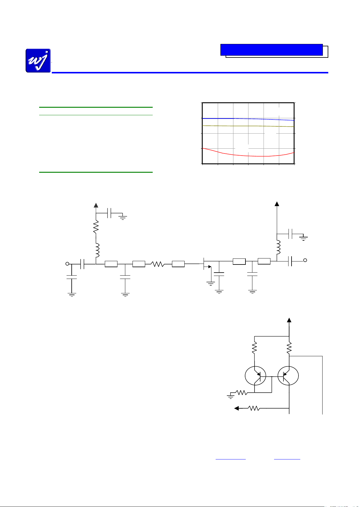
Application Circuit: 1960 MHz
R6
8.2 kΩ
Vdd = +8 V
Vgg = -4 V
UMT1N
6
1
5 2
4
3
Connected to Vdd
on App Circuit
Connected to Vgg
on App Circuit
R5
8.2 kΩ
R3
220 Ω
R4
2 Ω
1%
0603
Application Note
Special attention should be taken to properly bias up the HFETs. Power supply
sequencing is required to prevent the device from operating at 100% I
dss
for a prolonged
p
eriod of time and possibly causing damage to the device. It is recommended that for
the safest operation, the negative supply be “first on and last off.” With a negative gate
voltage present, the drain voltage can then be applied to the device. The gate voltage
can then be adjusted to have the device be used at the proper quiescent bias condition.
An optional temperature-compensation active-bias circuit is recommended for use with
the application circuit, which requires two standard voltage supplies +8V and -4V, an
d
is set for an optimal drain bias of +8V @ 100 mA. The circuit schematic, shown on the
right, uses dual PNP transistors to provide a constant drain current into the FET and also
eliminating the effects of pinchoff variation. Temperature compensation is achieved b
y
tracking the voltage variation with the temperature of the emitter-to-base junction of the
PNP transistors. Thus the transistor emitter voltage adjusts the voltage incident at the
gate of the FET so that the device draws a constant current, regardless of the
temperature. Two fixed voltage supplies are needed for operation. A Rohm dual
transistor, UMT1N, and a dual-chip resistor (8.2 kΩ) are recommended to minimize
board space and help decrease the current variability through R4 with the components
being matched to one another. The active-bias circuit can directly be attached to the
voltage supply ports in the circuit diagram as shown above (V
dd
and Vgg).
Vdd
+ 8 V @ 250 mA
FP1189
Sot-89
PIN 1
PIN 3
PIN 2,4
RF OUT
RF IN
L1
10 nH
C2
56 pF
Vgg
C3
2.2 pF
R1
20 Ω
C7
.018 µF
R2
5.1 Ω
L2
22 nH
C8
.018 µF
MLIN MLIN MLIN
MLIN
C5
0.6 pF
MLIN
C6
56 pF
C4
0.6 pF
C1
0.6 pF
Typical Specifications
Frequency 1960
S21 - Gain 16.5 dB
S11 - Input R.L. -23 dB
S22 - Output R.L. -6 dB
Output P1dB +28 dBm
Output IP3 +40 dBm
Noise Figure 3.8 dB
V
dd
+8.0 V
I
dd
1
100 mA
1 Idd is the quiescent current at small signal output levels. The current may increase
as the output power is increased near its compression point.
S-Pa rameters
-30
-20
-10
0
10
1930 1940 1950 1960 1970 1980 1990
Frequency (MHz)
S11, S22 (dB)
14
15
16
17
18
S21 (dB)
S21
S11
S22
 Loading...