

WJ Company FP101 Datasheet

WJ Communications, Inc. • Phone: 1-800-WJ1-4401 • FAX:408-577-6620 • e-mail:sales@wj.com • Web site: www.wj.com February 2002
FP101
Product Description
The FP101 is a high dynamic range FET packaged in a low cost surface mount package. The
combination of low noise figure and high IP3
at the same bias point makes it ideal for receiver and transmitter applications. The FP101
achieves +37 dBm OIP3 at a mounting temperature of 80˚C with an associated MTBF of
>100 years
3
.
All devices are 100% RF and DC tested. The
product is targeted for applications where high
linearity is required.
Product Features
•
50-3000 MHz Bandwidth
•
+37 dBm Output IP3
•
2.0 dB Noise Figure
•
13.5 dB Gain
•
+
26 dBm P1dB
•
MTBF >100 Years
•
SOT-89 SMT Package
Functional Diagram
4
123
Function Pin No.
Gate 1
Source 2
Drain 3
Source 4
High Dynamic Range FET
Specifications
DC Electrical Parameter Units Minimum Typical Maximum Condition
Saturated Drain Current, Idss mA 220 340 380 Vgs = 0 V
Transconductance, Gm mS 120
Pinch Off Voltage, Vp V -5.0 -3.7 Ids = 1.2 mA
RF Parameter Units Minimum Typical Maximum Condition
Small Signal Gain, Gss dB 11 13.5
Maximum Stable Gain, Gmsg dB 20.5
Third Order Output Intercept, OIP3 dBm 34 37
1 dB Compression Point, P1dB dBm 23 26
Noise Figure, NF dB 2.0
Test conditions unless otherwise noted:
1. RF and DC parameters measured under the following conditions unless otherwise noted.T = 22°C with Vds = 8 volts, Ids = 100 mA.Test frequency = 800 MHz, 50 ohm system.
2. OIP3 Measured with two tones at an output power of 2 dBm/tone separated by 10 MHz.The suppression on the largest IM3 product is used to calculate the OIP3 using a 2:1 rule.
3. MTBF calculated with channel temperature at 155˚C.
Recommended Maximum Ratings
Parameter Rating
Gate to Source Voltage -6.0 V
Drain to Source Voltage 9.0 V
Operating Case Temperature -40 to +80°C
Storage Temperature -55 to +125°C
RF Input Power (continuous) +12 dBm
Gate Current 6 mA
Maximum DC Power 0.9 W
Operation of this device above any of these parameters may cause permanent damage.
Ordering Information
Part No. Descr iption
FP101 High Dynamic Range FET
(Available in tape and reel)
The Communications Edge
™
Advanced Product Information
Actual Size
WJ Communications, Inc. • Phone: 1-800-WJ1-4401 • FAX:408-577-6620 • e-mail: sales@wj.com • Web site: www.wj.com February 2002
FP101
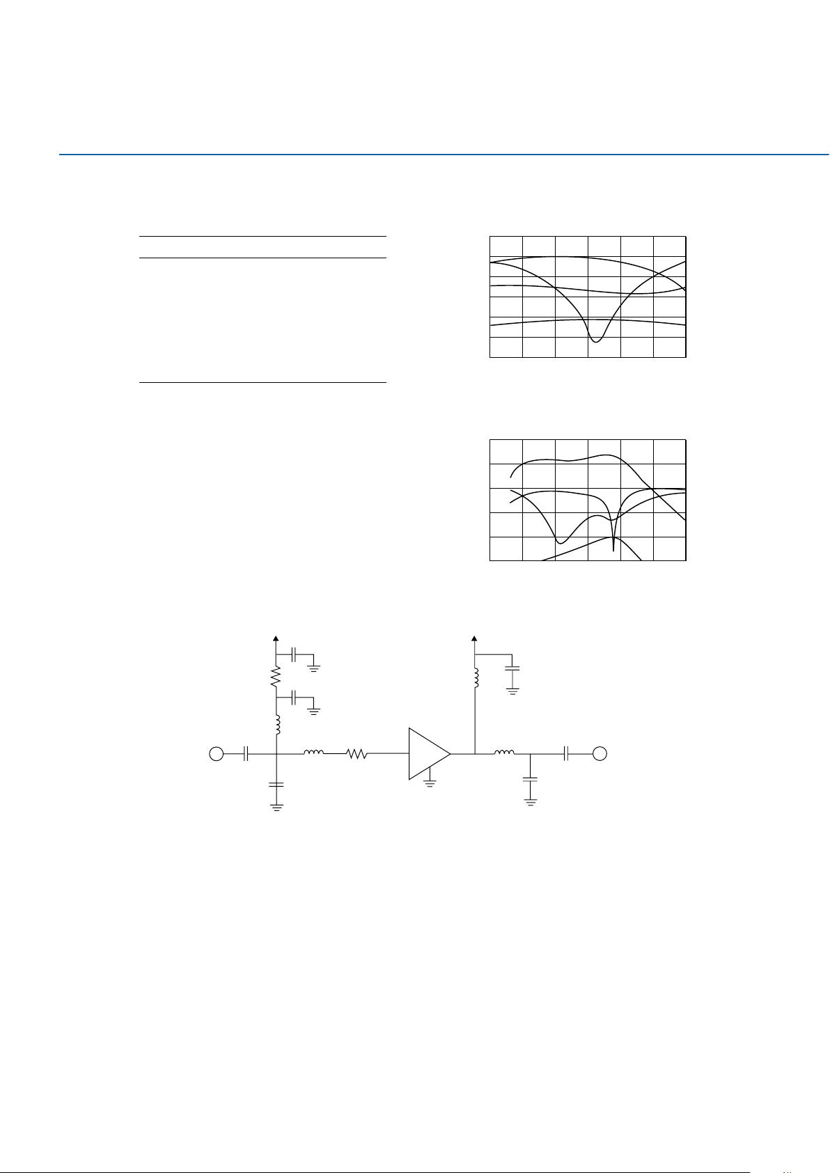
Application Circuit: 1800-1900 MHz
Frequency (MHz)
S21 (dB)
S11, S12, S22 (dB)
1700 1750 1800 1850 200019501900
S-Parameters
15
14
13
12
11
10
9
0
-5
-10
-15
-20
-25
-30
S21
S22
S11
S12
C6
68 pF
RF OUT
RF IN
C1
68 pF
C4
68 pF
C3
2.7 pF
L2
3.3 nH
L4
2.2 nH
C5
1.5 pF
L3
8.2 nH
R2
5.1 Ω
PIN 1 PIN 3
PIN 2,4
L1
18 nH
C2
68 pF
C2
0.018 µF
Vgs = 0.9 V
Vgs = +5 V
100mA
R1
51 Ω
FP101
3
Frequency (MHz)
(dB)
0 500 1000 1500 300025002000
Wideband S-Parameters
20
10
0
-10
-20
-30
S21
S12
S11
S22
Frequency 1850 MHz
S21 - Gain 13.9 dB
S11 - Input Return Loss 23.6 dB
S22 - Output Return Loss -13.5 dB
S12 - Isolation -20.9 dB
Output IP3
1
36.2 dBm
Output P1dB
4
23.3 dBm
Noise Figure 3.6 dB
Drain Bias 5 V @ 100 mA
Notes
1. OIP3 is measured with 2 tones at an output power of 10 dBm/tone
with 10 MHz spacing at 1850 MHz. The suppression on the largest
IM3 product is used to calculate OIP3 using a 2:1 slope rule. Test
parameters were taken at 25°C.
2. All components are 0603 size. Toko LL1608-FH chip inductors and
AVX ±0.1 pF tolerance capacitors (C3 and C5) were used in the
design. Other capacitor components are standard types. The overall
circuit size should be minimized as much as possible.
3. The FET should be mounted as shown in the FP101 datasheet.
4. The drain voltage can be increased up +8 V for increased output
power performance (higher P1dB). The gate voltage can be adjusted
so that the drain bias can be anywhere between 50 - 150 mA,
depending on the required performance using this device
5. More details are shown in WJ Application Note "FP101 PCS
Application Circuit"
Advanced Product Information
 Loading...