

WJ Company FH101 Datasheet
WJ Communications, Inc. • Phone: 1-800-WJ1-4401 • FAX: 408-577-6620 • e-mail: sales@wj.com • Web site: www.wj.com December2001
FH101
Product Description
The FH101 is a high dynamic range FET packaged in a low cost surface mount package. The
combination of low noise figure and high output IP3 at the same bias point makes it ideal for
receiver and transmitter applications. The FH101
achieves +36 dBm IP3 at a mounting temperature of 85˚C with an associated MTTF of >100
years. The package is a SOT-89. All devices are
100% RF & dc tested on a wafer.
The product is targeted for applications where
high linearity is required.
Product Features
•
36 dBm Output IP3
•
2.0 dB Noise Figure
•
18 dB Gain
•
18 dBm P1dB
•
DC-3 GHz Bandwidth
•
MTTF >100 Years
•
SOT-89 Surface Mount Package
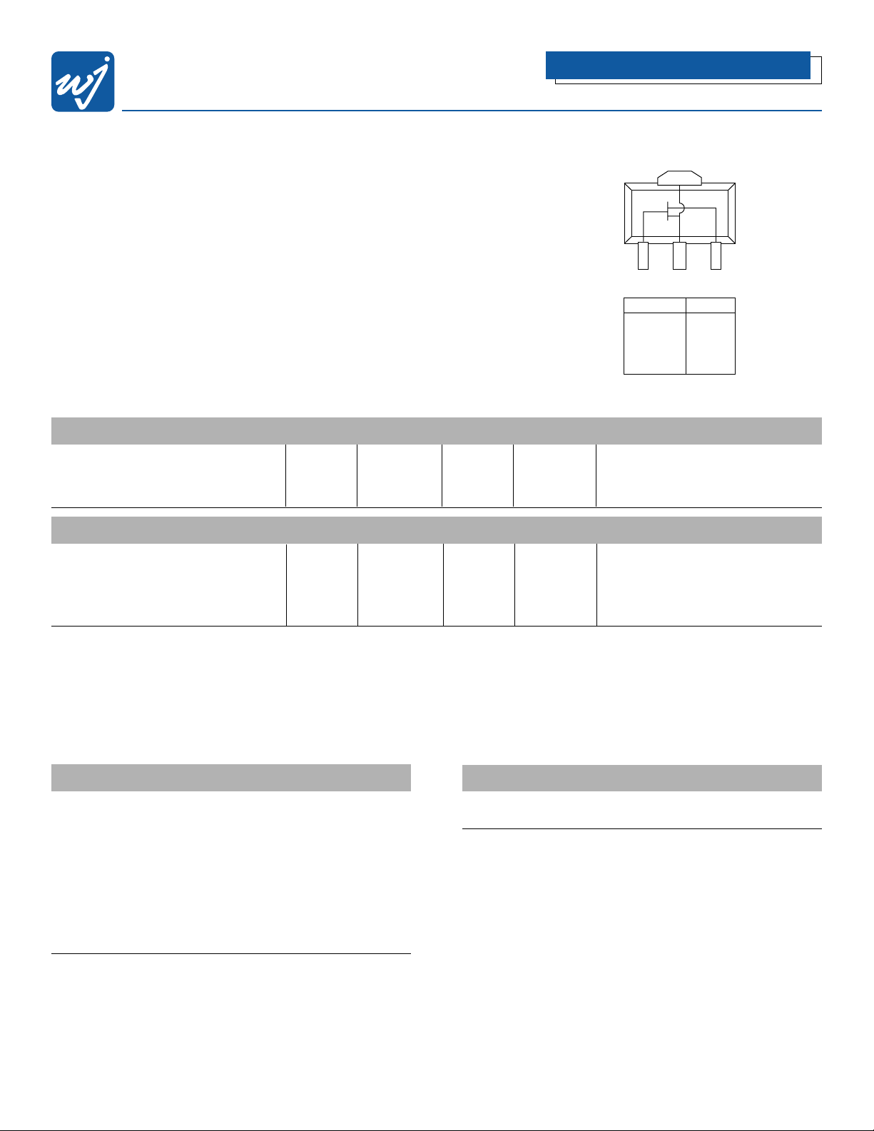
Functional Diagram
High Dynamic Range FET
Advanced Product Information
Specifications
DC Electrical Parameter Units Minimum Typical Maximum Condition
Saturated Drain Current, Idss mA 100 140 170 Vgs = 0V
Transconductance, Gm mS - 120 Pinch Off Voltage, Vp V -3.0 -1.5 - Ids = 0.6 mA
RF Parameter Units Minimum Typical Maximum Condition
Small Signal Gain, Gss dB 16 18 1 dB Compression Point, P1dB dBm - 18 -
Third Order Output Intercept, OIP3 dBm 32 36 -
Noise Figure, NF dB - 2.0 -
Notes:
1. DC parameters measured under the following conditions unless otherwise noted.
25°C with Vds = 5.0 volts
2. RF parameters measured under the following conditions unless otherwise noted.
25°C with Vds = 5.0 volts, Test frequency = 800 MHz, 50 ohm system.
3. 3OIP Measured with two tones at an output power of 5 dBm/tone separated by 10 MHz. The suppression on the largest IM3 product is used to calculate the 3OIP using a 2:1 slope r ule.
4. Device needs appropriate match to become unconditionally stable.
Ordering Information
Part No. Descr iption
FH101 High Dynamic Range FET
(Available in tape and reel)
The Communications Edge
™
Absolute Maximum Ratings
Parameter Rating Units
Drain to Source Voltage 8.0 Volt
Gate to Source Voltage -6.0 Volt
Gate Current 4.5 mA
Operating Case Temperature -40 to +85 °C
Storage Temperature -45 to +125 °C
Junction Temperature +155 °C
Thermal Resistance (θ
JC
) 85 °C/W
RF Input Power (continuous) +10 dBm
Operation of this device above any of these parameters may cause permanent damage.
4
123
Function Pin No.
Gate 1
Source 2
Drain 3
Source 4
 Loading...