

WJ Company FH1 Datasheet

WJ Communications, Inc. • Phone: 1-800-WJ1-4401 • FAX:408-577-6620 • e-mail:sales@wj.com • Web site: www.wj.com February 2002
FH1
Product Description
The FH1 is a high dynamic range FET packaged in a low cost surface mount package. The
combination of low noise figure and high output IP3 at the same bias point makes it ideal for
receiver and transmitter applications. The FH1
achieves +42 dBm OIP3 at a mounting temperature of 85˚C with an associated MTBF of
>100 years. The package is a SOT-89. All
devices are 100% RF and DC tested.
The product is targeted for applications where
high linearity is required.
Product Features
•
50-3000 MHz Bandwidth
•
+
42 dBm Output IP3
•
1.2 dB Noise Figure
•
18 dB Gain
•
+
21 dBm P1dB
•
Single or Dual Supply Operation
•
MTBF >100 Years
•
SOT-89 SMT Package
Functional Diagram
High Dynamic Range FET
Advanced Product Information
Ordering Information
Part No. Description
FH1 High Dynamic Range FET
(Available in tape and reel)
The Communications Edge
™
Absolute Maximum Ratings
Parameter Rating
Drain to Source Voltage +6.0 V
Gate to Source Voltage -6.0 V
Gate Current 4.5 mA
Operating Case Temperature -40 to +85°C
Storage Temperature -55 to +125°C
Input RF Power (continuous) +10 dBm
Operation of this device above any of these parameters may cause permanent damage.
Specifications
DC Electrical Parameter Units Min. Typical Max.
Saturated Drain Current, Idss mA 100 140 170
Transconductance, Gm mS 120
Pinch Off Voltage, Vp V -3.0 -1.5
RF Parameter Units Min. Typical Max.
Small Signal Gain, Gss dB 17 18
Max Stable Gain, Gmsg dB 23
Output IP3 dBm 38 42
Output P1dB dBm 21
Noise Figure, NF
7
dB 1.2
Notes:
1. DC and RF parameters measured under the following conditions unless otherwise noted.
25°C with Vds = 5.0 V, Vgs = 0 V, test frequency = 800 MHz, 50 Ω system.
2. OIP3 measured with two tones at an output power of 5 dBm/tone separated by 10 MHz.The
suppression on the largest IM3 product is used to calculate the OIP3 using a 2:1 slope rule.
3. Device needs appropriate match to become unconditionally stable.
4. Degradation of OIP3 occurs at low temperatures. Minimum typical OIP3 at -40°C is +36 dBm.
5. Idss is measured with Vgs = 0 V.
6. Pinch off voltage is measured when Ids = 0.6 mA.
7. Measured with Vds = 3.3 V, 50% Idss.
Typical Parameters
Parameter Units Typical
Frequency MHz 900 1900
S21 dB 19.0 16.0
S11 dB -10.7 -12.3
S22 dB -9.7 -17.2
Output IP3 dBm +44.0 +39.6
Output P1dB dBm +21.8 +22.1
Noise Figure dB 2.7 3.1
Drain Bias Supply 5 V @ 140 mA
Gate Bias 0 V
Typical parameters reflect performance in an application circuit.
Actual Size
4
123
Function Pin No.
Gate 1
Source 2
Drain 3
Source 4
WJ Communications, Inc. • Phone: 1-800-WJ1-4401 • FAX:408-577-6620 • e-mail: sales@wj.com • Web site: www.wj.com February 2002
FH1
Advanced Product Information
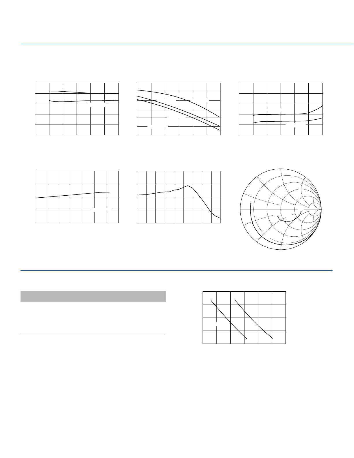
Performance Charts (Vds = 5.0 V, Ids = 150 mA, T = 22°C, 50 ohm system)
Thermal Specifications
Parameter Rating
Operating Case Temperature -40 to +125°C
Thermal Resistance (Maximum) 59°C/W
Junction Temperature +155°C
(Recommended Maximum)
Notes:
1.Thermal Resistance determined at Maximum Tab Temperature and Maximum Power
Dissipation.
2. Recommended Maximum Junction Temperature insures a MTBF of 1 million hours.
OIP3 vs. Frequency
50
40
30
20
OIP3 (dB)
10
0
0 .5 1 1.5 2 32.5
5V 100% Idss
3.3V 50% Idss
Frequency (GHz)
OIP3 vs. Temperature OIP3 vs. Power Out
50
45
40
OIP3 (dBm)
35
30
-40 -20 0 20 40 60 10080
Temperature (°C)
5V, 100% Idss
Gain vs. Temperature
23
21
19
17
Gain (dB)
15
13
11
0 .5 1 1.5 2 2.5 3
50
45
40
OIP3 (dBm)
35
30
02 4 6 8 1210 14 16 18
Gain at +22°C
Gain at +85°C
5V, 100% Idss
Frequency (GHz)
Output Power (dBm)
Gain at -40°C
NF vs. Frequency
5
4
3
NF (dB)
2
1
0
0 .5 1 1.5 2 32.5
5V 100% Idss
3.3V 50% Idss
Frequency (GHz)
S-Parameters
2.05
2.05
S22
S11
0.05
3
0.05
MTBF vs. Temperature
11
10
S11 and S22
MTBF vs. Temperature
9
10
8
10
7
10
MTBF (hours)
Ground Tab
6
10
5
10
50 75 100 125 150 175 200
Temperature (°C)
Junction
 Loading...