

WJ Company CV111-1 Datasheet
d
y
CV111-1
PCS/DCS-band Single-Branch Downconverter
Product Features
• High dynamic range downconverter
with integrated LO driver and IF
amplifiers
• +27 dBm Input IP3
• +12 dBm Input P1dB
• 11.5 dB Noise Figure
• RF: 1710 - 1910 MHz
• IF: 70 - 250 MHz
• Low-side LO downconverter
• Single supply operation (+5 V)
• 6 x 6 mm QFN SMT package
Actual Size
CV
The Communications Edge TM
Product Description
The CV111-1 is a high-linearity downconverter
designed to meet the performance, functionality,
and cost goals of current and next generation
mobile infrastructure basestations.
It is ideally suited for high dynamic range
receiver front ends. The module is implemente
in reliable GaAs MESFET technology and
requires only a small 6x6 mm footprint.
Typical applications include frequenc
downconversion used in CDMA/GSM/TDMA,
CDMA2000, W-CDMA, and EDGE 2.5G and
3G mobile base transceiver stations.
Preliminary Information
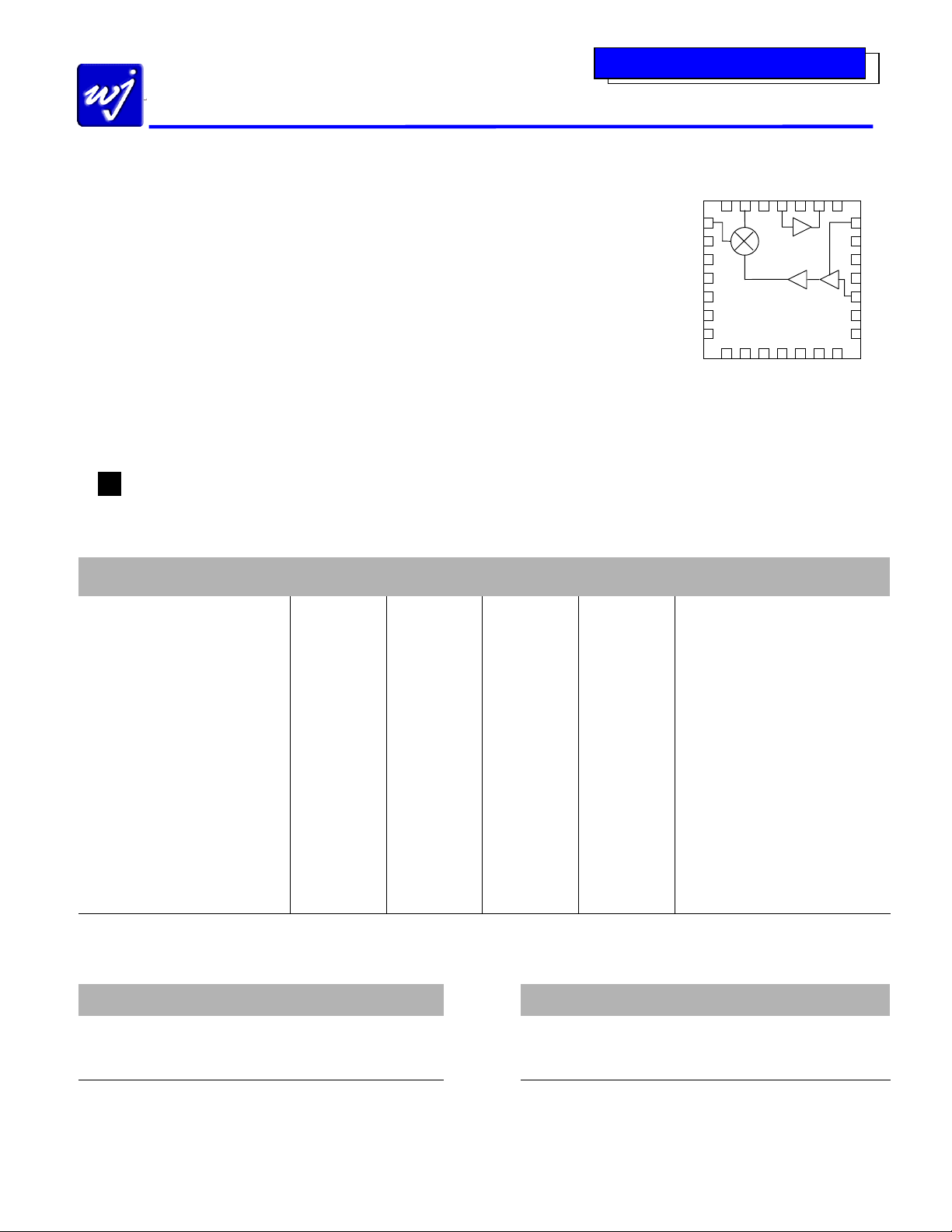
Functional Diagram
23
25
27
RF
8
IF
IF amp
LO driver amp
Top View
1
21
+
Vcc
17
Specifications1
Parameters Units Minimum Typical Maximum Comments
RF Frequency Range MHz 1710
LO Frequency Range MHz 1460
IF Frequency Range MHz 70
IF Bandwidth %
SSB Conversion Gain dB 8
Input IP3 dBm
Input IP2 dBm
Input 1 dB Compression Point dBm
Noise Figure dB
LO Input Drive Level dBm -2.5
LO-RF Isolation dB
LO-IF Isolation dB
Return Loss: RF Port dB
Return Loss: LO Port dB
Return Loss: IF Port dB
Operating Supply Voltage V +4.75
Supply Current mA
1
Specifications when using application specific circuit with a low side LO = 0 dBm in a downconverting application at 25°C.
20
10
+27
+32
+12
11.5
0
9
30
14
14
14
+5
190
1910
1840
250
12
∆f = 1 MHz @ RFin = 0 dBm / tone
12.5
+2.5
P
P
= 0 dBm
LO
= 0 dBm
LO
+5.25
230
Absolute Maximum Rating2 Ordering Information
Parameters Rating Part No. Description
Operating Case Temperature
-40° to +85 °C
Storage Temperature -65° to +100 °C
Maximum Junction Temperature +150 °C
2
Operation of this device above any of these parameters may cause permanent damage.
WJ Communications, Inc • Phone 1-800-WJ1-4401 • FAX: 408-577-6620 • e-mail: sales@wj.com • Web site: www.wj.com
CV111-1 PCS/DCS-band Single-Branch Downconverter
Specifications and information are subject to change without notice
This document contains information on a new product.
May 2002
The Communications Edge TM
CV111-1
PCS/DCS-band Single-Branch Downconverter
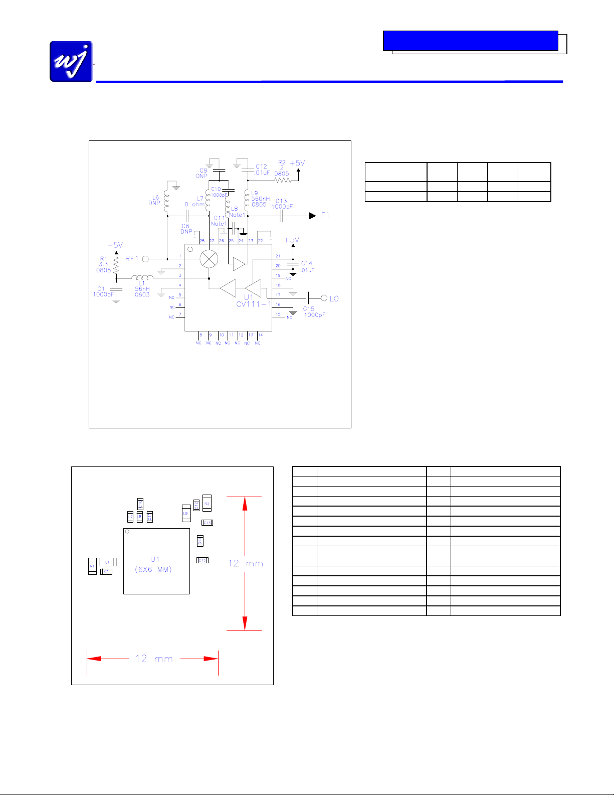
Application Circuit
Note 1:
IF Freq (MHz)
70 – 90 100 100 20 20
230 - 250 47 47 2.7 2.7
All components are of size 0603 or 0402 unless otherwise noted
DNP represents: Do Not Place.
Preliminary Information
L4
(nH)
L8
(nH)
C4
(pF)
C11
(pF)
Assembly Layout
WJ Communications, Inc • Phone 1-800-WJ1-4401 • FAX: 408-577-6620 • e-mail: sales@wj.com • Web site: www.wj.com
Pin FUNCTION Pin FUNCTION
1 Channel 1 RF Input 15 N/C
2 GND 16 GND
3 +5 V 17 LO input
4 GND 18 GND
5 N/C 19 N/C
6 N/C 20 GND
7 N/C 21 +5 V
8 N/C 22 GND
9 N/C 23 Channel 1 IF Amp Output / +5 V
10 N/C 24 GND
11 N/C 25 Channel 1 IF Amp Input
12 N/C 26 GND
13 N/C 27 Channel 1 IF Mixer Output
14 N/C 28 GND
Functional Pin Layout
Specifications and information are subject to change without notice
This document contains information on a new product.
May 2002
 Loading...