

WJ Company AL1 Datasheet
WJ Communications, Inc. • Phone: 1-800-WJ1-4401 • FAX:408-577-6620 • e-mail:sales@wj.com • Web site: www.wj.com
February 2002
AL1
Product Description
The AL1 is a high intercept, low-noise amplifier
designed for wide dynamic range receiver applications. Exceptional low noise performance and
low input VSWR can be achieved simultaneously with the use of low cost SMT components to implement the input-matching network. The AL1 operates from a single +5 V
supply voltage, has a DC blocking capacitor on
the RF output, and is available in a low cost
SOIC-8 package. The AL1 is designed for wireless local loop, wireless LAN, and other applications within the ISM band.
Product Features
•
1.4 dB Noise Figure
•
23 dB Gain
•
+20 dBm Output IP3
•
45 dB Reverse Isolation
•
Single +5.0 V Bias Supply
•
SOIC-8 SMT Package
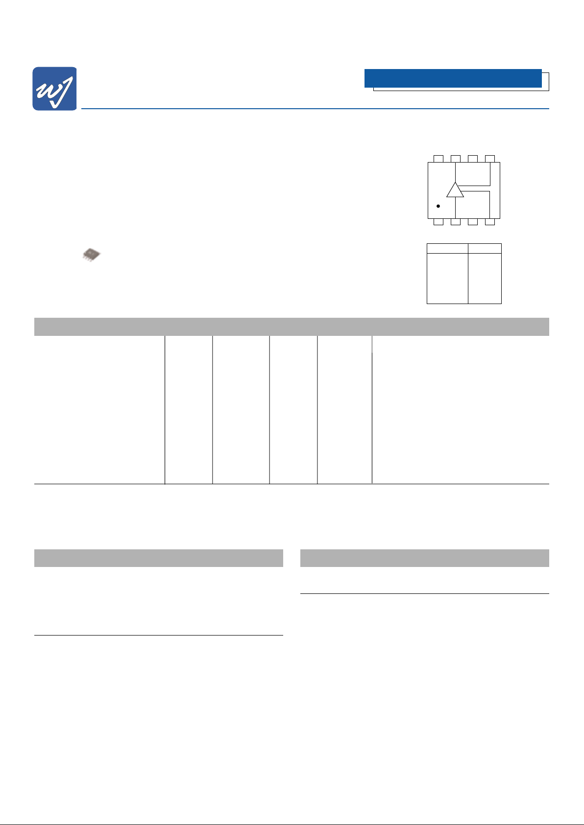
Functional Diagram
Absolute Maximum Ratings
Parameter Rating
Operating Case Temperature -40 to +85°C
Storage Temperature -55 to +125°C
Supply Voltage +8 V
Input RF Power (Instantaneous) +16 dBm
Junction Temperature 155°C
Operation of this device above any of these parameters may cause permanent damage.
Ordering Information
Part No. Description
AL1 Low Noise Amplifier
(Available in tape and reel)
Function Pin No.
Ground 1, 3, 6, 8
RF In 2
RF Out 7
VDD1 4
VDD2 5
8765
1234
Low Noise Amplifier
Specifications
Parameter Units Minimum Typical Maximum Condition
Frequency MHz 2300-2500
S21 - Gain dB 21 23
S11-Input Return Loss dB -7.3 -8.5
S22-Output Return Loss dB -9.5 -15
S12-Isolation dB 35 45
Gain Temperature Coefficient dB/˚C -0.025
Noise Temperature Coefficient dB/˚C 0.0067
Output IP3 dBm 18 +20
Output P1dB dBm +10
Noise Figure dB 1.4 1.8
Operating Current Range mA 27 45 60
Test conditions unless otherwise noted:
1.Tests performed in Application Circuit Fixture with external input match.
2. Electr ical specification: T = 25˚C, Vdd = 5.0 V, unless otherwise specified.
3.Typical values are measured at 2.4 GHz.
The Communications Edge
™
Advanced Product Information
Actual Size
AL1
Advanced Product Information
WJ Communications, Inc. • Phone: 1-800-WJ1-4401 • FAX:408-577-6620 • e-mail:sales@wj.com • Web site: www.wj.com
February 2002
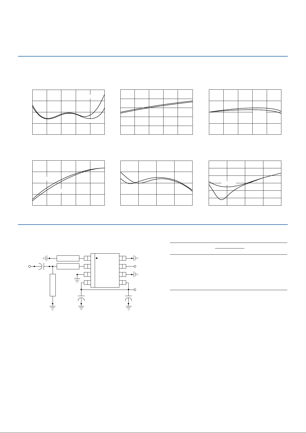
Performance Charts (Measured in Application Circuit)
Noise Figure (dB)
Frequency (GHz)
Vdd = 3.6 V
Vdd = 5.0 V
Vdd = 3.6 V
Vdd = 5.0 V
Vdd = 5.0 V
2.0 2.2 2.4 2.6 3.02.8
OIP3 vs. Frequency Gain vs. FrequencyNoise Figure vs. Frequency
OIP3 (dBm)
Frequency (GHz)
Frequency (GHz)
2.0 2.2 2.4 2.82.6 3.0
Frequency (GHz)
2.0 2.2 2.4 2.6 2.8 3.0
2.5
2.0
1.5
1.0
0.5
Output Return Loss vs. Frequency
2 2.25 2.5 2.75 3
Output Return Loss (dB)
0
-5
-10
-15
-25
-20
-30
25
23
21
19
17
15
Gain (dB)
30
25
15
20
10
Isolation (dB)
Frequency (GHz) Frequency (GHz)
2.0 2.2 2.4 2.6 3.02.8
Input Return Loss vs. FrequencyIsolation vs. Frequency
Input Return Loss (dB)
2 2.25 2.5 2.75 3
-30
-70
-60
-50
-40
0
-20
-15
-10
-5
Vdd = 3.6 V
Vdd = 5.0 V
Vdd = 3.6 V
Vdd = 5.0 V
Vdd = 3.6 V
Vdd = 5.0 V
Vdd = 3.6 V
Application Circuit Schematic
8
7
6
5
1
2
3
4
Zo = 64.5 Ω, Φ = 10.4° plus
70 pH via inductance
Zo = 87.3 Ω, Φ = 18.1° plus
70 pH via inductance
Zo = 64.5 Ω
Φ = 15.0°
RF IN
RF OUT
1.8 pF
1000 pF 1000 pF
Vdd = 5 V
Phases given at f = 2.4 GHz
Noise Parameters
T = 25°C,Vdd = +5.0 V
Frequency NF
O
ΓOPT G
assoc
(GHz) (dB) Mag Ang Rn/Z
O
(dB)
1.95 0.87 0.72 62.4 0.44 21.8
2.10 0.84 0.68 68.4 0.38 22.3
2.25 0.91 0.66 73.1 0.34 22.6
2.40 0.93 0.63 79.2 0.30 23.1
2.55 1.02 0.30 84.5 0.27 23.5
2.70 1.05 0.54 90.6 0.24 23.9
2.85 1.15 0.52 96.6 0.22 24.1
Note: Noise parameters are measured without external input match. The reference
planes are located at outer ends of the package leads, shown as the
dimension 236 mil in SOIC-8 package outline.
 Loading...