

WJ Company AH3-PCB, AH3 Datasheet
WJ Communications, Inc. • Phone: 1-800-WJ1-4401 • FAX:408-577-6620 • e-mail:sales@wj.com • Web site: www.wj.com February 2002
AH3
Product Description
The AH3 is a high dynamic range amplifier for
IF requirements. The product achieves low
noise figure and high output IP3 at the same
bias point, making it ideal for receiver and
transmitter applications. In addition, the device
is internally matched for 50 ohms in a low cost
SOT-89 package. The AH3 is manufactured
using GaAs MESFET technology and boasts an
MTBF of >100 years
3
at a mounting temperature
of 85˚C. The package is a SOT-89. All devices
are 100% RF and DC tested.
Product Features
•
50-450 MHz
• +40 dBm Output IP3
• No Matching Elements Required
• 3.0 dB Noise Figure
•
13.5 dB Gain
• +20 dBm P1dB
• MTBF >100 Years
• SOT-89 SMT Package
• Single Bias Supply (+5 V )
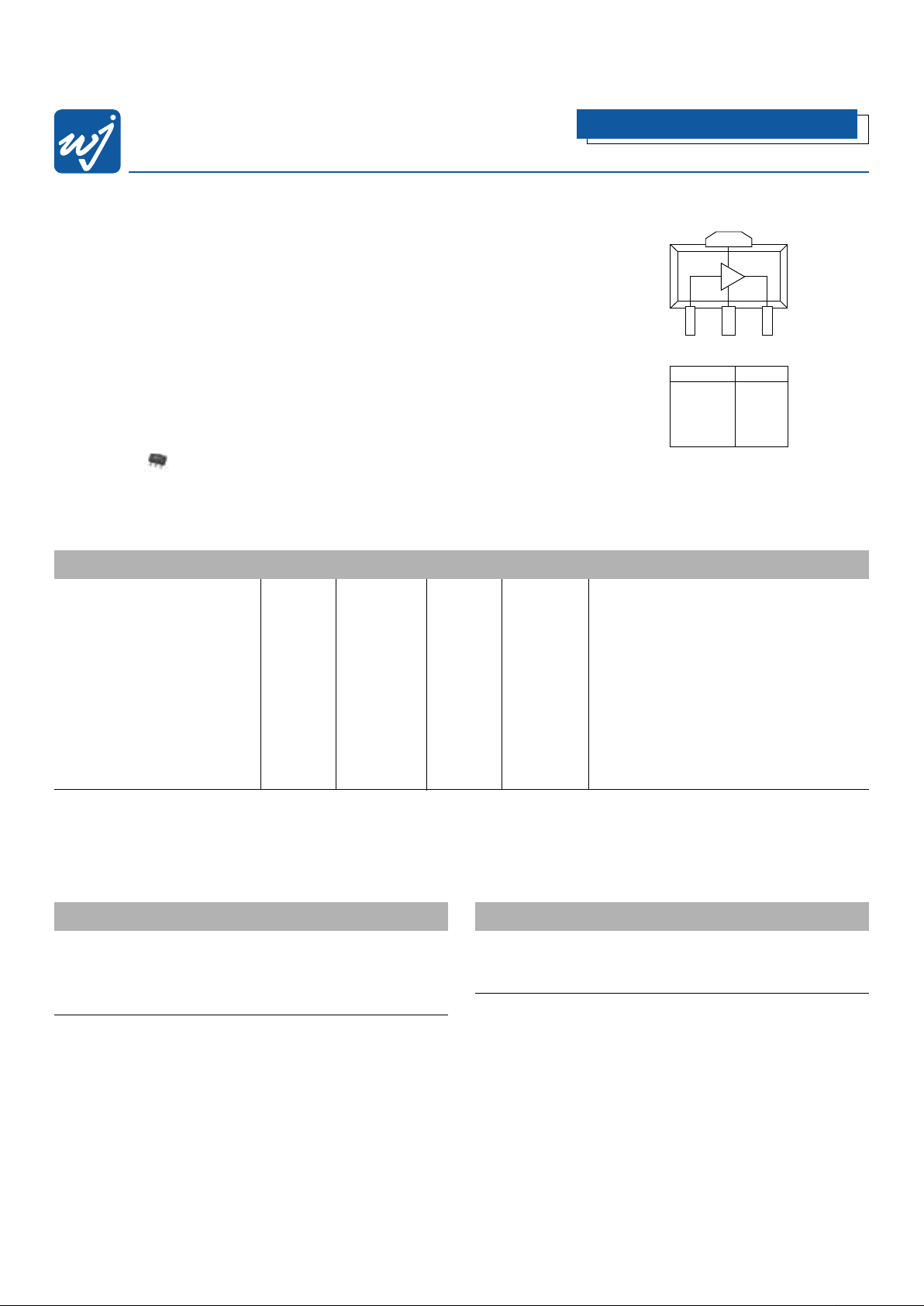
Functional Diagram
Absolute Maximum Ratings
Parameter Rating
Operating Case Temperature -40 to +85°C
Storage Temperature -55 to +125°C
Supply Voltage +6.0 V
Input RF Power (continuous) +10 dBm
Operation of this device above any of these parameters may cause permanent damage.
Ordering Information
Part No. Description
AH3 High Dynamic Range Amplifier
(Available in tape and reel)
AH3WB-PCB Fully Assembled Application Circuit
4
123
Function Pin No.
Input 1
Ground 2
Output/Bias 3
Ground 4
High Dynamic Range Gain Block
Specifications
Parameter Units Minimum Typical Maximum Condition
Frequency Range MHz 50-450
S21 - Gain dB 12 13.5 16
S11 - Input Return Loss
1
dB -10
S22 - Output Return Loss dB -20
Output IP3 dBm +37 +40
Output P1dB dBm +20
Noise Figure
1
dB 4.5 50 MHz
Noise Figure dB 3.0 450 MHz
Operating Current Range mA 120 150 180 Vdd = 5.0 V
Supply Voltage V 5
Test conditions unless otherwise noted, T = 25˚C, Vdd = 5.0 V, 50 Ω system, 800 MHz.
1. S11 and Noise Figure can be improved using an optional input matching network.
2. OIP3 measured with 2 tones at an output power of 5 dBm/tone separated by 10 MHz.The suppression on the largest IM3 product is used to calculate OIP3 using a 2:1 slope rule.
3. MTBF calculated with ground lead temperature at 85˚C.
The Communications Edge
™
Actual Size
WJ Communications, Inc. • Phone: 1-800-WJ1-4401 • FAX:408-577-6620 • e-mail: sales@wj.com • Web site: www.wj.com
February 2002
AH3
Performance Charts (Vds = 5 V. Ids = 150 mA, T = 22°C, unmatched device in a 50 ohm system)
10
9
10
8
10
7
10
6
10
5
50 75 100 125 150 175 200
Temperature (°C)
MTBF (hours)
MTBF vs. Temperature
Junction
Ground Tab
Gain and Return Loss (dB)
Frequency (MHz)
50 150 250 350 500450
Gain and Return Loss vs. Frequency
20
10
0
-10
-20
-40
-30
Gain
Vd = 5.0, I = 150 mA
Input Return Loss
Output Return Loss
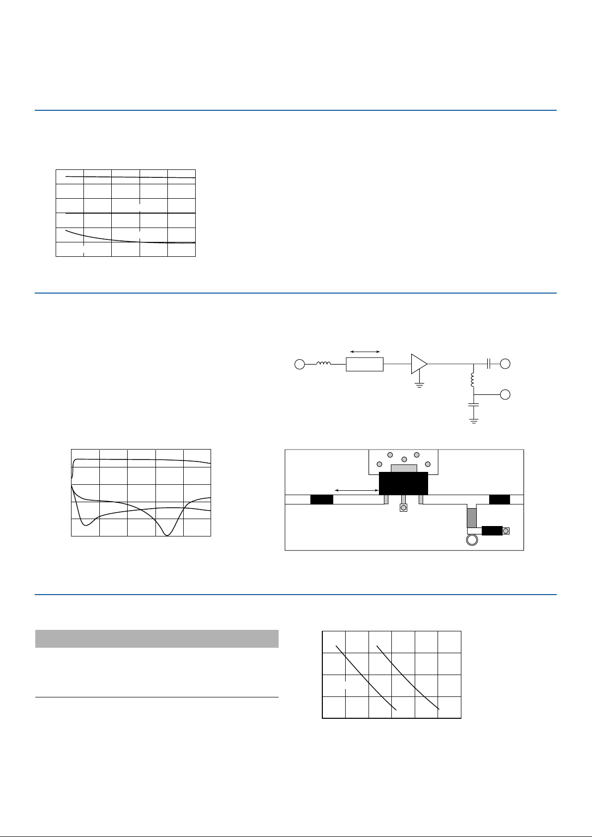
Application Circuit: 50 to 450 MHz
Frequency (MHz)
Magnitude (dB)
0 200 400 600 1000800
S-Parameters
20
10
0
-10
-20
-30
Typical Specifications
Frequency 50 MHz 450 MHz
Magnitude S21 13.7 dB 13.7 dB
Magnitude S11 -8.3 dB -13.3 dB
Magnitude S22 -18.0 dB -15.2 dB
OIP3 36 dBm 40 dBm
Noise Figure 3.6 dB 2.7 dB
Bias Vds = 5.0 V, Id = 150 mA
FR4 Board Layout (T = 14 Mils)
Schematic
S21
S11
S22
Z = 50 ohm
100 mil
AH3
C = 1000 pF
RF OUT
RF IN
DC+5.0 V
C = 560 pF
L = 390 nH
L = 12 nH
100 mil
SOURCE
0603 Package
C = 1000 pF
0603 Package
C = 560 pF
Package 1008
L = 390 nH
Coilcraft
0603 Package
L = 12 nH
+5.0 V
GATE DRAIN
3 or more Via
Grounds req.
All Trans. Lines Z = 50 Ohm
SOURCE
AH3
NOTE: The application circuit is designed for wide bandwidth. For narrow band applications,
S11 and S21 can be improved with an input shunt microstrip element to ground.
Thermal Specifications
Parameter Rating
Operating Case Temperature -40 to +85°C
Thermal Resistance (Maximum) 59°C/W
Junction Temperature +155°C
(Recommended Maximum)
Notes:
1.Thermal Resistance determined at Maximum Tab Temperature and Maximum Power
Dissipation.
2. Recommended Maximum Junction Temperature insures a MTBF of 1 million hours.
3. Refer to WJ Application Note “AH3 Temperature Effects on Reliability” for more information.
 Loading...