

WJ Company AH201-PCB-900, AH201-PCB-1900, AH201 Datasheet
m
r
r
AH201
Medium Power, High Linearity Amplifier
Product Features
• 400 – 2200 MHz
• +30 dBm P1dB
• +47 dBm Output IP3
• 17 dB Gain @ 900 MHz
• MTBF >100 Years
z
• Single Positive Supply (9-12V)
•
Internally Matched
•
24dBm IS-95 Channel Power
@ -45dBc ACPR
Actual Size
Specifications
The AH201 is a 1W driver amplifier that offers
excellent dynamic range in a low cost, 6x6m
surface mount package. This device can be biased as
low as +9V for lower power applications and as high
as +12V for improved P1dB and OIP3 performance.
The backside metalization allows excellent thermal
dissipation while allowing visible evidence of solde
reflow throughout the bottom of the package on a
SMT board. Superior thermal design allows the
product an MTBF of over 100 years at a mounting
temperature of +85ºC. All devices are 100% RF &
DC tested.
The product is targeted for use as driver amplifiers fo
wireless infrastructure where high linearity and
medium power is required.
Product Description
Parameters
Frequency Range MHz 400-2200
S21 - Gain dB 15
S11 - Input Return Loss dB
S22 - Output Return Loss dB
Noise Figure dB
Output P1dB dBm
Output IP3 dBm
Operating Current Range mA 310 330 370
Supply Voltage V 11
Thermal Resistance Rth 14
Test conditions unless otherwise noted.
1. T = 25ºC, Vdd = 11V, Frequency = 800 MHz, 50 Ohm system.
2. 3OIP measured with two tones at an output power of 10 dBm/tone separated by 10 MHz.
The suppression on the largest IM3 product is used to calculate the 3OIP using a 2:1 rule.
Units Min Typ. Max
-9.5
-10
4
+30
+47
The Communications Edge TM
Preliminary Product Information
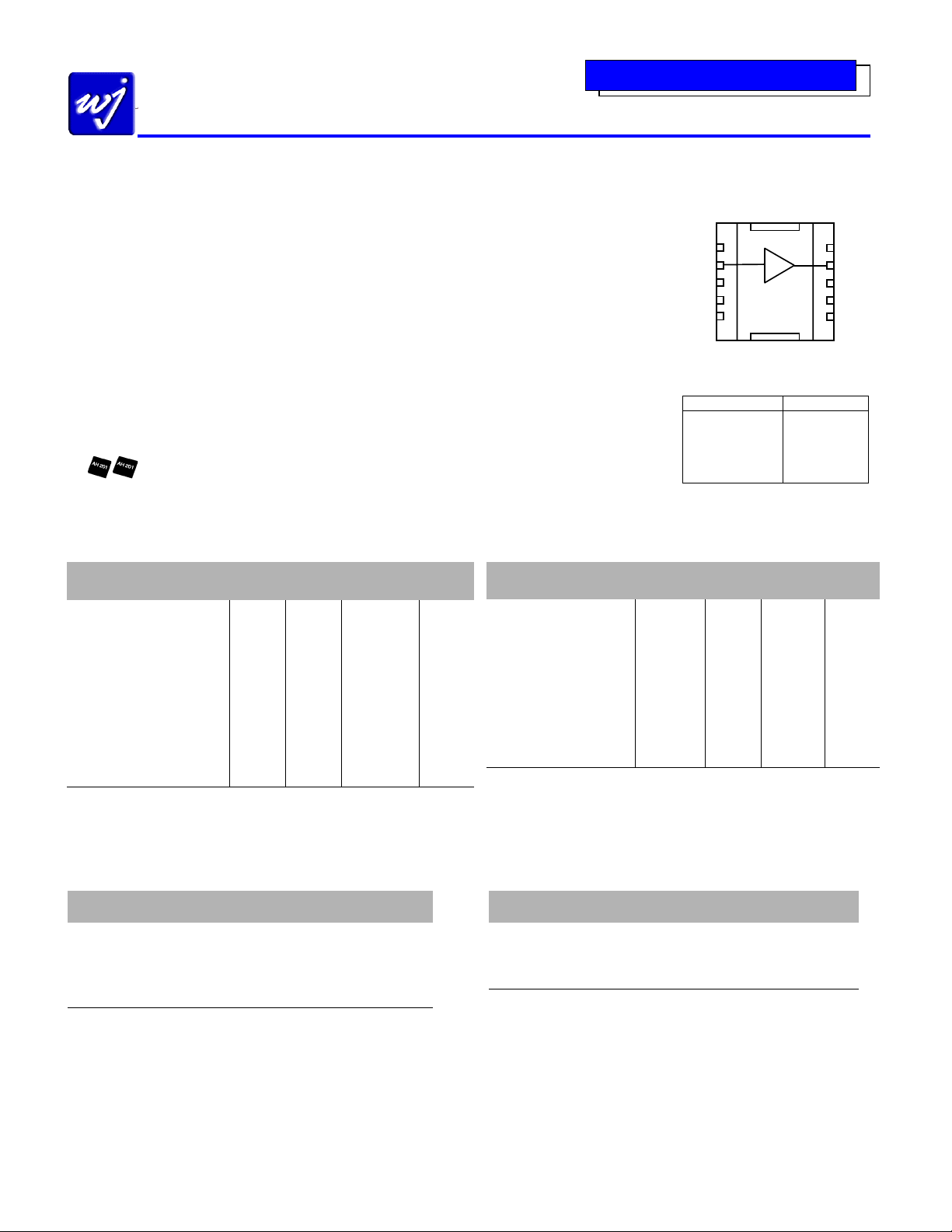
Functional Diagram
1
5
10
6
Top View
Function Pin No.
Input 2
Output/Bias 9
Ground 1, 2, 3, 5
Ground 6, 7, 8, 10
Not Connected 4
Typical Specifications
Parameters Units Typical
Frequency MHz 900 1900 2200
S21 - Gain dB 17 15 14
S11 - Input R.L. dB -13 -9.5 -9.3
S22 - Output R.L. dB -15 -9.5 -9.0
Noise Figure dB 3.8 4.3 4.4
Output P1dB dBm +30.0 +29.5 +29.3
Output IP3 dBm +47 +47 +47
IS-95 Channel Power
@ -45dBc ACPR
Typical parameters reflect performance in an application circuit.
1. T = 25ºC, Vdd = 11V
2. 3OIP measured with two tones at an output power of 10 dBm/tone separated by 10 MHz.
The suppression on the largest IM3 product is used to calculate the 3OIP using a 2:1 rule.
dBm +24 +23.6 +23.5
Recommended Maximum Rating Ordering Information
Parameters Rating Part No. Description
Operating Case Temperature
Storage Temperature
DC Voltage +15 V
RF Input Power (continuous) +20 dBm
Junction Temperature
-40 to +85 °C
-40 to +125 °C
+155° C
This document contains information on a new product.
WJ Communications, Inc • Phone 1-800-WJ1-4401 • FAX: 408-577-6620 • e-mail: sales@wj.com • Web site: www.wj.com
AH201 Med. Power High Linearity Amp.
AH201-PCB-900 400-1000 MHz Evaluation Board
AH201-PCB-1900 1600-2200 MHz Evaluation Board
Specifications and information are subject to change without notice
(Available in Tape & Reel)
May 2002
y
AH201
Medium Power, High Linearity Amplifier
Application Circuit: 900 MHz and 1900 MHz
Typical Specifications
Frequency MHz 900 1900 2200
S21 - Gain dB 17 15 14
S11 - Input R.L. dB -13 -9.5 -9.3
S22 - Output R.L. dB -15 -9.5 -9.0
Noise Figure dB 3.8 4.3 4.4
Output P1dB dBm +30.0 +29.5 +29.3
Output IP3 dBm +47 +47 +47
IS-95 Channel Power
@ -45dBc ACPR
CIRCUIT SCHEMATIC
INPUT MATCH
RF IN
C1
56 pF
C2
L1
dBm +24 +23.6 +23.5
VS = +11 V
= 330 mA
I
D
L2
22 nH
PIN 2 PIN 9
AH201
56 pF
C3
C4
56 pF
RF OUT
C5
0805
1000 pF
DC BIAS
C6
1206
.018 µF
The Communications Edge TM
Preliminary Product Information
GND
AH201
L1
C3
RF In
C1 C2
Board Material: 14 mil GETEK (εr = 4.1)
Line Width: 28 mil
Line Spacing: 36 mil
Notes:
• Via holes are omitted for clarity.
• The microstrip line is weakly co-planer. Ground planes
around it are not necessary for operation of the AH201.
• Adequate heat sinking is required for the device.
Further mounting instructions will be shown in the
“Mounting Configuration” section of this datasheet on
the next revision for the datasheet.
• The pin configuration must be soldered accordingl
(shown on the “Functional Diagram”).
• The 900 MHz application circuit board is labeled as
AH201-PCB-900.
• The 1900 MHz and 2200 MHz application circuit board
is labeled as AH201-PCB-1900.
L1
C4
C5
C6
Vs
RF Out
900 MHz 1900 MHz 2200 MHz
L1 = 3.3 nH L1 = 0 Ω L1 = 0 Ω
C2 = 2.2 pF C2 = no load C2 = no load
AH201-PCB-900 AH201-PCB-1900 AH201-PCB-1900
This document contains information on a new product.
WJ Communications, Inc • Phone 1-800-WJ1-4401 • FAX: 408-577-6620 • e-mail: sales@wj.com • Web site: www.wj.com
Specifications and information are subject to change without notice
May 2002
 Loading...