

WJ Company AH102-PCS, AH102-PCB, AH102 Datasheet
WJ Communications, Inc. • Phone: 1-800-WJ1-4401 • FAX: 408-577-6620 • e-mail: sales@wj.com • Web site: www.wj.com March 2002
AH102
Preliminary Product Information
Product Description
The AH102 is a medium power gain block
that offers excellent dynamic range in a low cost
surface mount package. The combination of a
signal supply voltage and an internally matched
device makes it ideal for both narrow band and
broadband applications. Superior thermal
design allows the product to achieve +45 dBm
IP3 performance at a mounting temperature of
+85°C with an associated MTBF of >10
7
hours.
Product Features
•
350-3000 MHz Bandwidth
•
+45 dBm Output IP3
•
13 dB Gain
•
+27 dBm P1dB
•
MTBF >107Hours
•
Internally Matched
•
Multiple Bias Voltages
(+7.0 to +9.0 V)
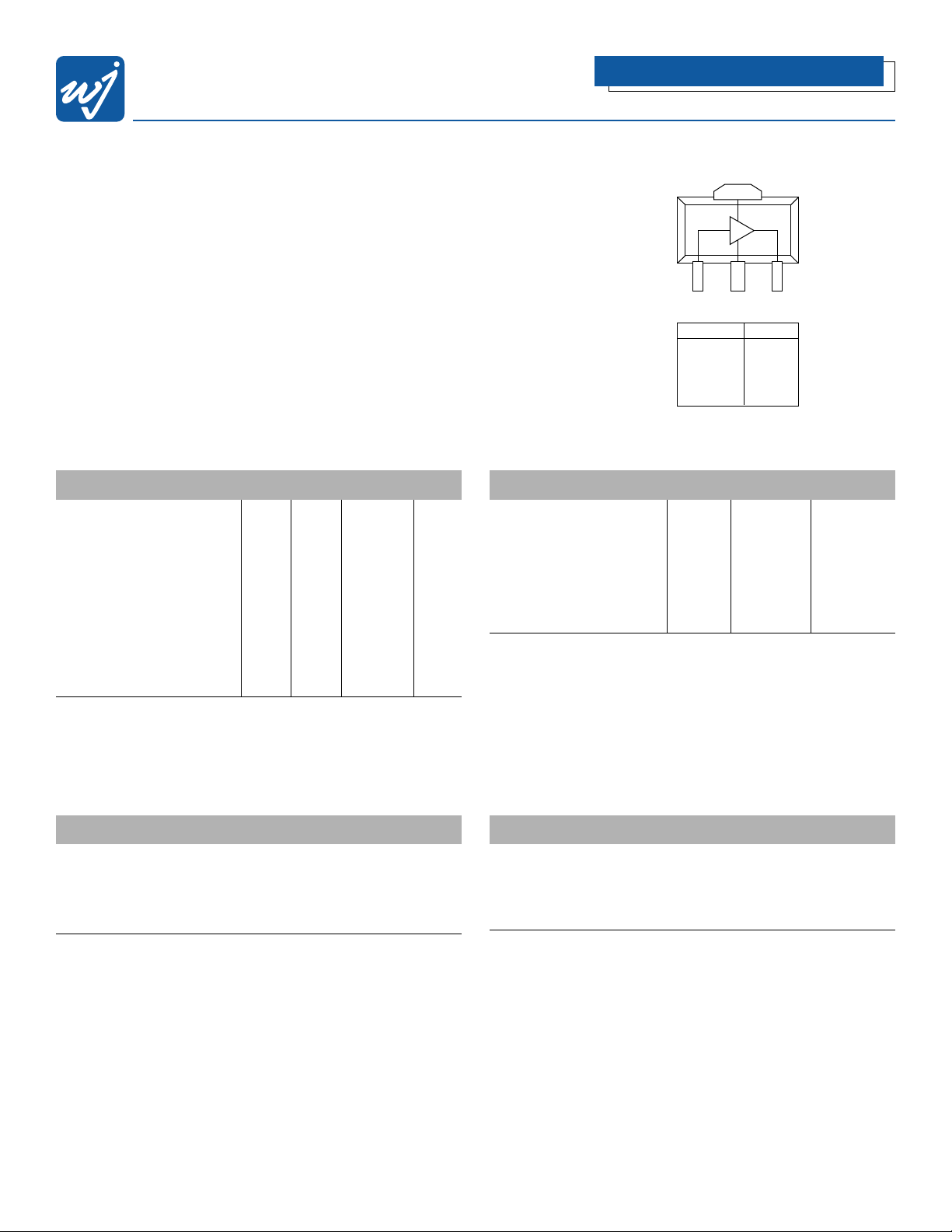
Functional Diagram
Medium Power, High Linearity Amplifier
Specifications
Parameter Units Min. Typical Max.
Frequency Range MHz 350-3000
S21 - Gain dB 12.5 13
S11 - Input Return Loss dB -10
S22 - Output Return Loss dB -10
Noise Figure dB 4.5
Output P1dB dBm +27
Output IP3 dBm 43 +45
Operating Current Range mA 170 200 230
Supply Voltage V 9.0
Test conditions unless otherwise noted.
1. T = 25°C, Vdd = 9.0 V, Freq = 800 MHz, 50 ohm system.
2. 3OIP Measured with two tones at an output power of 8 dBm/tone separated by 10 MHz. The
suppression on the largest IM3 product is used to calculate the 3OIP using a 2:1 slope rule.
Typical Parameters
Parameter Units Typical
Frequency MHz 900 1900
S21 dB 13.9 13.5
S11 dB -17.4 -15.2
S22 dB -16.5 -15.0
Output IP3 dBm 46.2 46.0
Noise Figure dB 3.1 3.8
Typical parameters reflect AH102 application circuit.
Absolute Maximum Ratings
Parameter Rating
Operating Case Temperature -40 to +85°C
Storage Temperature -55 to +125 °C
DC Voltage +11 V
RF Input Power (continuous) +17 dBm
Ordering Information
Part No. Description
AH102 Medium Power High Linearity Amplifier
(Available in tape and reel)
AH102-PCB Cell Cellular Application Circuit
AH102-PCS/u PCS/UMTS Application Circuit
The Communications Edge
™
This document contains information on a new product.
Specifications and information are subject to change without notice.
4
123
Function Pin No.
Input 1
Ground 2
Output Bias 3
Ground 4
WJ Communications, Inc. • Phone: 1-800-WJ1-4401 • FAX: 408-577-6620 • e-mail: sales@wj.com • Web site: www.wj.com March 2002
AH102
Preliminary Product Information
Thermal Data
Parameter Rating
Operating Case Temperature -40 to +85°C
Thermal Resistance (Maximum) 25°C/W
Junction Temperature +155°C
(Recommended Maximum)
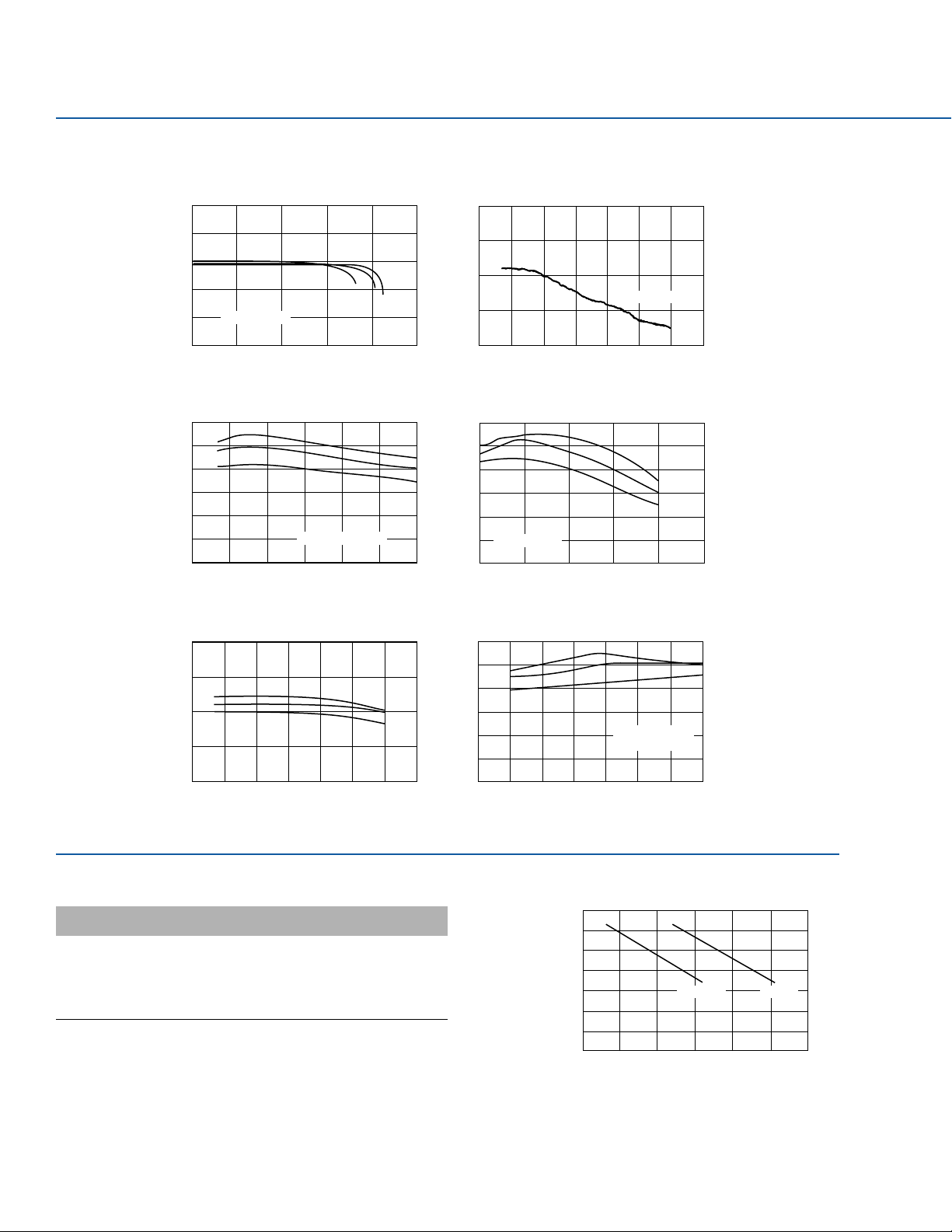
Performance Charts (Vds = 9 V, Ids = 200 mA, T = 22°C, unmatched device in a 50 ohm system)
18
16
14
12
Gain (dB)
10
RF = 900 MHz
8
10
50
9 V
45
8 V
7 V
40
35
OIP3 (dBm)
30
25
20
0 500 1000
35
30
25
P1dB (dB)
20
15
0
500
Gain vs Pout
7 V
14 18
Pout (dB)
22
OIP3 vs Frequency
Pout = 8 dBm/tone
1500 2500
Frequency (MHz)
2000
P1dB vs Frequency
1000
2000
1500
Frequency (MHz)
2500
8 V
9 V
26 30
9 V
8 V
7 V
3000
35003000
18
16
14
Gain (dB)
12
10
0 500 1000
1500
Frequency (MHz)
2000
7 V, 8 V, 9 V
2500 3000
OIP3 vs Pout
Gain vs Frequency
50
45
40
35
OIP3 (dBm)
30
RF = 900 MHz
25
20
0 5 10 15
Pout (dB)
20 25
OIP3 vs Temperature
50
45
9 V
8 V
40
7 V
35
OIP3 (dBm)
30
25
20
-60 -40 -20 0 20 40 60 80
Temperature (°C)
Pout = 8 dB/tone
RF = 900 MHz
3500
9 V
8 V
7 V
1.00E+09
1.00E+08
1.00E+07
1.00E+06
1.00E+05
MTBF (Hrs)
1.00E+04
1.00E+03
1.00E+02
MTBF vs Temperature
Ground Tab
50 75 100 125 150
Temperature (°C)
Junction
175 200
 Loading...