

WJ Company AG402-89, AG402-86PCB, AG402-86, AG402-89PCB Datasheet
h
p
h
d
n
The Communications Edge TM
AG402
InGaP HBT Gain Block
Preliminary Product Information
Product Description
• DC - 5000MHz
• +17 dBm P1dB at 900MHz
• +32 dBm OIP3 at 900MHz
• 15 dB Gain at 900MHz
• Single Voltage Supply
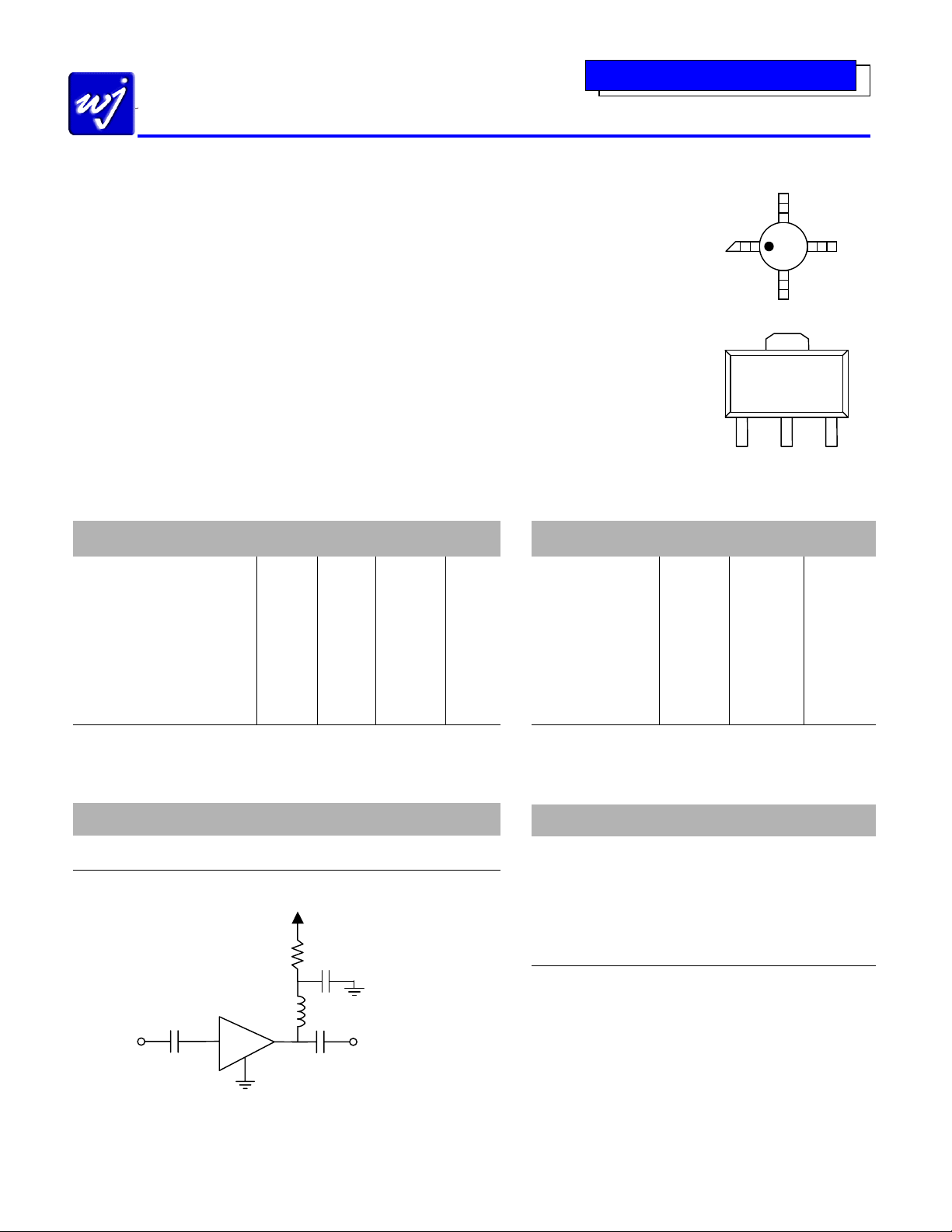
• SOT-86 or SOT-89 SMT
Package
•
Internally matched to 50 Ω
The AG402 is a general-purpose buffer amplifier that offers hig
dynamic range in a low-cost surface-mount package. At 900 MHz,
the AG402 typically provides 15 dB of gain, +32 dBm Output IP3,
and +17 dBm P1dB. The device combines dependable
erformance with consistent quality to maintain MTBF values
exceeding 100 years at mounting temperatures of +85°C and is
housed in a SOT-86 and SOT-89 industry standard SMT packages.
The AG402 consists of Darlington pair amplifiers using the hig
reliability InGaP/GaAs HBT technology process technology an
only requires DC-blocking capacitors, a bias resistor, and a
inductive RF choke for operation.
The broadband MMIC amplifier can be directly applied to various
current and next generation wireless technologies such as GPRS,
GSM, CDMA, W-CDMA, and UMTS. In addition, the AG402
will work for other various applications within the DC to 5 GHz
frequency range such as CATV and fixed wireless.
Specifications
Parameters1 Units Min Typ Max
Frequency Range MHz DC-5000
S21 - Gain dB 15
S11 - Input Return Loss dB -15
S22 - Output Return Loss dB -15
Output P1dB dBm +17
Output IP3 dBm +32
Noise Figure dB 4.3
Device Voltage V 5.0
Device Current mA
Test conditions unless otherwise noted
1. T = 25ºC, Supply Voltage = +6 V, R
2. 3OIP measured with two tones at an output power of 0 dBm/tone separated by 10MHz. The
suppression on the largest IM3 product is used to calculate the 3OIP using a 2:1 rule.
= 16 Ω, Frequency = 900MHz, 50 Ω System.
bias
60
Absolute Maximum Ratings
Functional Diagram Product Features
GND
RF IN
AG42
GND
RF OUT
AG402-86
GND
AG402
RF IN
GND RF OUT
AG402-89
Typical Parameters
Parameter1 Units Typical
Frequency MHz 900 1900
S21 dB 15 14
S11 dB -15 -12
S22 dB -25 -20
Output P1dB dBm +17 +16
Output IP3 dBm +32 +29
Noise Figure dB 4.3 4.5
Supply Voltage V 6 6
Device Current mA
1. Data represents typical performance in an application board with
T = 25ºC, Vs = +6 V, and R
= 16 Ω in a 50 Ω system.
bias
60
Ordering Information
60
Parameters Rating
Operating Case Temperature
Storage Temperature
Operation of this device above any of there parameters may cause permanent damage
Application Circuit
R1
RF IN
C1
Blocking
Capacitor
AG402
16 Ω
L1
RF
Choke
-40 to +85 °C
-40 to +125 °C
VS = +6 V
IS = 60 mA
C3
Bypass Capacitor
RF OUT
C2
Blocking
Capacitor
Part No. Description
AG402-86 InGaP HBT Gain Block
SOT-86 Style Package
AG402-89 InGaP HBT Gain Block
AG402-86PCB Fully Assembled Application Board
AG402-89PCB Fully Assembled Application Board
(Available in Tape & Reel)
SOT-89 Style Package
(Available in Tape & Reel)
This document contains information on a new product.
WJ Communications, Inc • Phone 1-800-WJ1-4401 • FAX: 408-577-6620 • e-mail: sales@wj.com • Web site: www.wj.com
Specifications and information are subject to change without notice
June 2002
The Communications Edge TM
AG402
InGaP HBT Gain Block
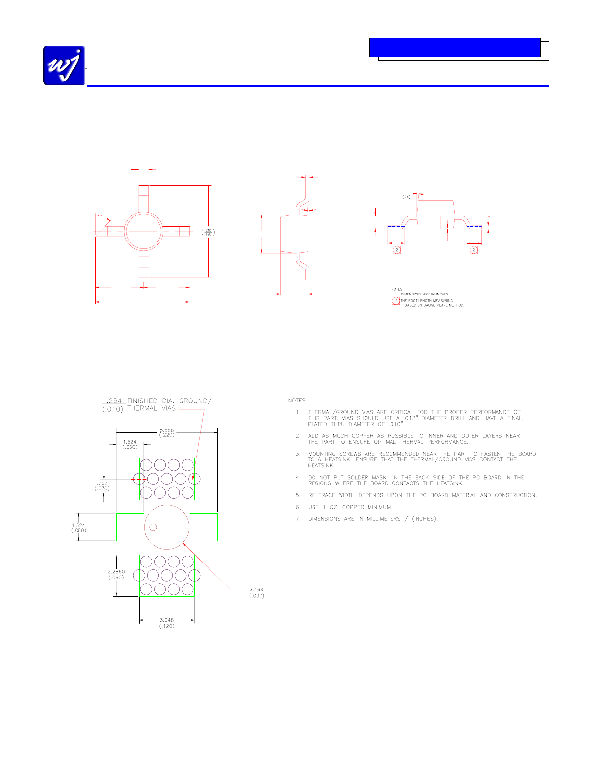
AG402-86 Package Information
Outline Drawing
.021 ± .004
.008 ± .002
45°
.085 ± .005
0° - 8°
.026 ± .005
.037 ± .010
(.195 - .215)
.100 ±.005
.060 ± .005
.105 ±.005
Land Pattern Mounting Configuration Notes
Preliminary Product Information
7°
.006 (Guage Plane)
Seating Plane
+.0020
.002
-.0015
.032 ± .010
(3X)
This document contains information on a new product.
WJ Communications, Inc • Phone 1-800-WJ1-4401 • FAX: 408-577-6620 • e-mail: sales@wj.com • Web site: www.wj.com
Specifications and information are subject to change without notice
June 2002
 Loading...