Watkins-Johnson: The Cell Extenders
Power Amplifiers
SA1083
CDMA 10-Watt
1.93 GHz to 1.99 GHz
Linear Power Amplifier Module
The Wireless Edge
™
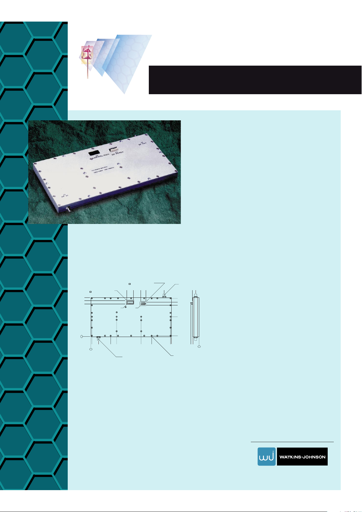
CONNECTOR, J2, RF OUTPUT
SMA, FEMALE
CONNECTOR, J1, RF INPUT
SMA, FEMALE
8X MOUNTING HOLES,
COUNTERBORED FOR
4–40 PAN HEAD SCREW
CONNECTOR, J3, DC POWER
4 PIN, .045 PINS, .156 CENTERS
CONNECTOR, J4, CONTROL/DATA
10 PIN, .025 PINS, .100 CENTERS
4.48
PIN 1 PIN 1
5.28 6.17 6.80 9.15
.70
.67.89
2X .36
2X 4.86
4X 2.50
2X .14
10.009.862X 7.506.083.212X 2.50
.85.14
4.35
4.00
5.00
4.53
4.17
OUTLINE DRAWING
WJ Wireless Products: 1-800-WJ1-4401• FAX: 650-813-2447 • e-mail: wireless.info@wj.com.
W
atkins-Johnson’s SA1083 Power Amplifier
provides exceptional linearity for CDMA
digital modulation applications. Utilizing WJ’s
GaAs amplifiers driving bipolar transistors in the
class AB output stage, the SA1083 achieves a
high third-order intercept point combined with
superior efficiency when compared to an equiva-
lent power class A amplifier. Special non-linear
design techniques are utilized to minimize
unwanted adjacent channel power. To aid top
level system diagnostics and reliability, the unit
includes alarms to identify if an active part fails
or if a poor load is presented to the RF output.
In the event that a fault is detected or to simply
save DC power, a digitally controlled shutdown
is provided. The amplifier is protected from
thermal overload by an internal temperature
sensor which triggers a digital alarm and shuts
down the power stages if the baseplate tempera-
ture rises above 95°C. An integral logarithmic
power detector measures the output power of
the amplifier over a 16 dB dynamic range.
■
10 Watts CDMA IS-95
■
+48 dBm P1dB
■
45 dB Gain
■
-30°C to +85°C

Watkins-Johnson: The Cell Extenders
Power Amplifiers
The Wireless Edge
™
SA1083
CDMA 10-Watt 1.93 GHz to 1.99 GHz
Linear Power Amplifier Module
WATKINS-JOHNSON COMPANY • 3333 Hillview Avenue • Palo Alto, CA 94304-1223
Specifications
Parameters (Baseplate Temperature: -30°C to +85°C) Typical Level Specified Limits
Frequency 1.930-1.990 GHz
P
out
at 1 dB Gain Compression +48 dBm
Gain (Small signal at 25°C) 45 ± 1.0 dB
Gain Variation over Temp (-30°C to +85°C) ±1.5 dB
CDMA1Adjacent Channel Power Rejection (ACPR)
First Channel ACP Rejection (885 KHz offset from fo, in a 30 KHz integration BW)
P
out
< 40 dBm (CDMA)
1
-47 dB -45 dB
Spurious Suppression Outside Frequency Block
a) ACP level at 1.25 to 2.25 MHz offset from fo, in a 12.5 KHz integration BW,
P
out
< 40.0 dBm (CDMA)
1
-14 dBm -12 dBm max
2
b) ACP level at 2.25 to 3.25 MHz offset from fo, in a 1.0 MHz integration BW,
P
out
< 40.0 dBm (CDMA)
1
-13 dBm -12 dBm max
2
Third-Order 2-Tone Output Intermodulation Product Rejection
(P
out
= +37 dBm per CW tone) -35 dB -30 dB max
Maximum Noise Figure 5.0 dB 6.5 dB
Input and Output Impedence 50 ohm
Return Loss (1.930-1.990 GHz)
Input and Output -20 dB -15 dB
Load Mismatch Sustainable without Damage 3.0:1
Output Power Monitor
a) P
out
= +40 dBm CW 4.5 V 5.0 V max, 4.0 V min
b) P
out
= +32 dBm CW 2.5 V 3.0 V max, 2.0 V min
c) P
out
= +24 dBm CW 0.5 V 1.0 V max, 0.0 V min
Supply Voltages +24 V 23.5-26.5 V
Maximum Supply without Damage, +24 Volt Supply +28 VDC
Maximum DC Current, +24 Volt Supply 7.2 amps 7.5 amps
DC Power Dissipation, +24 Volt Supply 175 watts 180 watts
RF Connectors SMA Female
Stability (No spurious outputs above -50 dBc) Unconditionally stable for all loads
Size (Heat sink not included) 0.67" (H), 5.0" (W), 10.0" (L)
Weight (Heat sink not included) 40 oz. max
Note: 1. CDMA adjacent power and spurious measurements are made using a Rohde & Schwarz SMIQ03 service in an IS-95 forward Link mode.
2. 1.0 dB minimum loss between power amplifier output and antenna port of top level assembly assumed for IS-95 compliance.
 Loading...