

查询AH103供应商
AH103
High Gain, High Linearity ½ Watt Amplifier Product Information
Product Features
• 60 – 2700 MHz
• +27 dBm P1dB
• +46 dBm Output IP3
• 28.5 dB Gain @ 900 MHz
• Excellent ACPR
• MTTF > 100 Years
• SOIC-8 Pkg w/ heat slug
Applications
•
Mobile Infrastructure
•
W-LAN / ISM / RFID
•
MDS / MMDS Infrastructure
Specifications
Product Description
The AH103 is a high gain, high linearity ½-Watt
amplifier. This device is comprised of two individual
MMIC amplifiers internally and can be used with an
external interstage match for any of the mobile
infrastructure frequency bands. The dual-stage
amplifier achieves up to +46 dBm IP3 performance
with 28.5 dB gain.
The device conforms to WJ Communications’ long
history of producing high reliability and quality
components. The AH103 has an associated MTTF of
a minimum of 100 years at a mounting temperature
of 85°C. All devices are 100% RF & DC tested.
The product is targeted for use as driver amplifiers
for wireless infrastructure where high performance
and high linearity are required.
Typical Performance
The Communications Edge TM
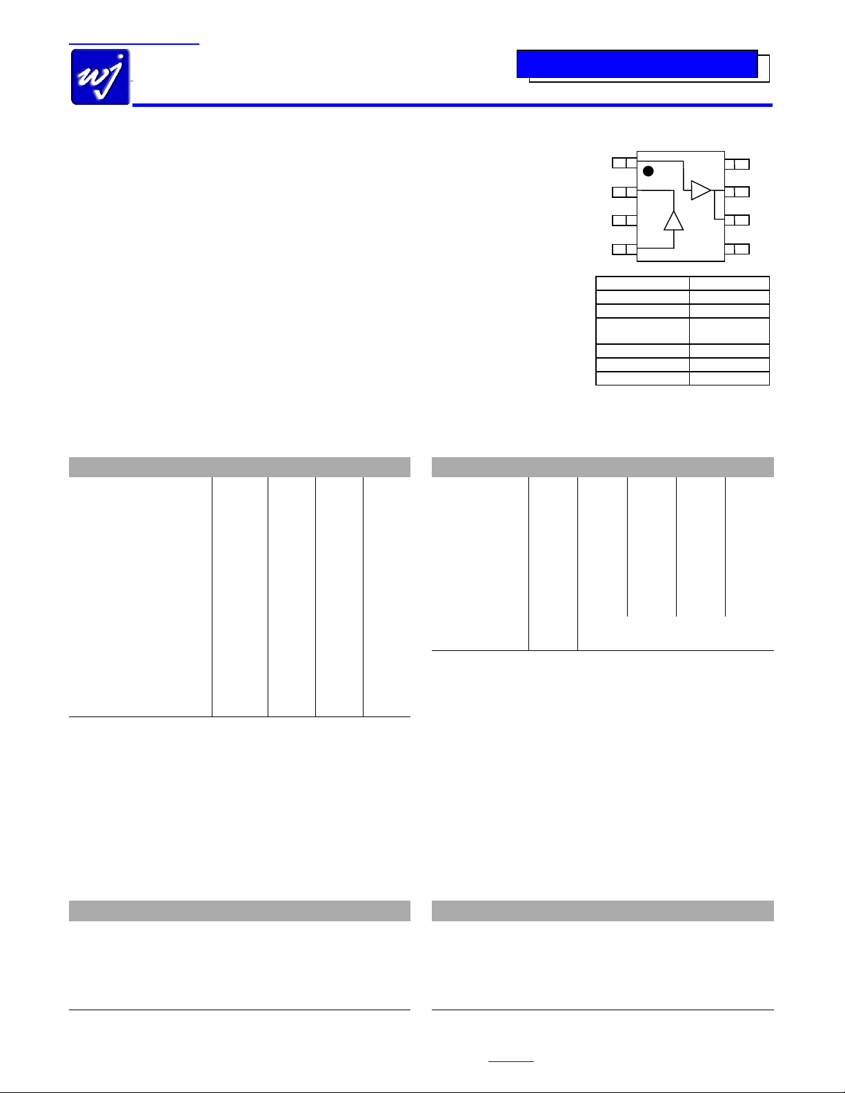
Functional Diagram
1
2
AMP 1
3
4
Function Pin No.
Amp2 in 1
Amp1 out / Bias 1 2
Ground
RF in (Amp1 in) 4
RF out (Amp2 out) 6
Bias 2 7
AMP 2
3, 5, 8,
Backside copper
8
7
6
5
Parameter Units Min Typ Max
Frequency Range (2) MHz 60 800 2700
Gain dB 26.5
Input Return Loss dB
Output Return Loss dB
Output P1dB dBm +26
Output IP3 (3)
IS-95 Channel Power (4)
@ -45 dBc ACPR
Noise Figure dB 2.9
Supply Voltage (Amp1) V
Supply Voltage (Amp2) V
Operating Current (Amp1) mA 55
Operating Curre n t ( A mp2 ) mA 170
Thermal Resistance (5) °C / W
Junction Temperature (6) °C
Test conditio ns unles s otherwise noted.
1. T = 25ºC, Vdd1 = +4.5 V, Vdd2 = +9 V, Frequency = 800 MHz in a tuned application circuit.
2. The frequency of operation & bandwidth is determined by the external interstage match.
3. 3OIP measured with two tones at an out put power of +10 dBm/tone separated by 10 MHz. T he
suppression on the largest IM3 product is used to calculate the 3OIP using a 2:1 rule.
4. IS-95, 9 Channels Forward, Pk/Avg Ratio = 11.5 dB at a .001% probability
±750 kHz offset, 30 kHz BW, Channel BW = 1.23 MHz, frequency = 880 MHz.
5. The worst-case junction temperature for a g iven ground tab temperature can be calculated by
multiplying the thermal resistance with the tot al package power d issipation and adding it to the t ab
temperature. ie. At 85°C case temperature for a typ ical device, the worst-case junction temperature
would be = 85°C + (9 V * 0.2 A + 4.5 V * 0.075 A) = 129°C.
6. The junction temperature ensures a minimum MTTF rating of 1 million hours of usage.
dBm +43
dBm
28.5
20
11
+27
+46
+21
+4.5
+9
75
200
100
230
20.6
160
Parameter Units Typical
Frequency MHz 900 1900 2140 2400
S21 dB
S11 dB
S22 dB
Output P1dB dBm
Output IP3 dBm
Channel Power
@ -45 dBc ACPR / ACLR
Noise Figure dB
Supply Bias 1
Supply Bias 2 +9 V @ 200 mA
7. Typical parameters reflect performance in an application circuit.
8. An IS-95 signal is used for 915 / 1960 MHz. A 3GPP W-CDMA signal is used for 2140 MHz.
dBm
28.5 26 25
-15 -12 -11
-11 -11 -14
+27 +26.5 +26.5
+46 +45 +45
+21 +20 +17.2
2.9 3.7 3.5 3.6
+4.5 V @ 75 mA
24.7
-12
-17
+26
+43.3
Absolute Maximum Rating Ordering Information
Parameter Rating Part No. Description
Operating Case Temperature
Storage Temperature
DC Voltage (pin 2) +6 V
DC Voltage (pin 6, 7) +11 V
RF Input Power (continuous) 4 dB above Input P1dB
Junction Temperature
Operation of this device above any of these parameters may cause permanent damage.
WJ Communications, Inc • Phone 1-800-WJ1-4401 • FAX: 408-577-6621 • e-mail: sales@wj.com • Web site: www.wj.com November 2003
-40 to +85 °C
-55 to +125 °C
+220°C
AH103 High Gain ½ Watt Amplifier
AH103-PCB900 0.7 – 1.0 GHz Evaluation Circuit
AH103-PCB1750 1.7 – 1.8 GHz Evaluation Circuit
AH103-PCB1900 1.8 – 2.0 GHz Evaluation Circuit
AH103-PCB2140 2.1 – 2.2 GHz Evaluation Circuit
(available in tape and reel)
Specifications and information are subject to change without notice
AH103
The Communications Edge TM
High Gain, High Linearity ½ Watt Amplifier Product Information
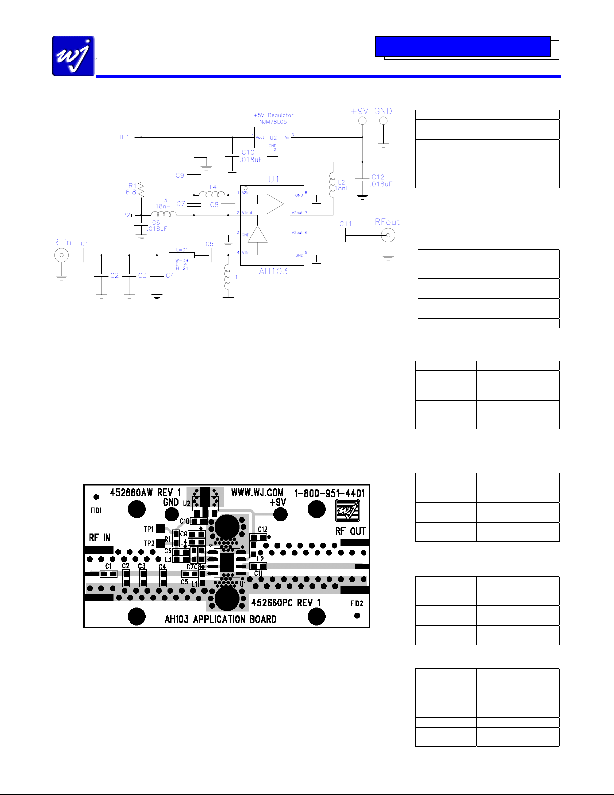
Application Circuit
Ref. Desig. Component
R1
L2, L3 18 nH chip inductor
C6, C10, C12
U1 WJ AH103 Amplifier
U2
5. All components are of size 0603.
6.
Ref. Desig. Component
L1 10 nH chip inductor
L4 5.6 nH chi p inductor
C1
C5, C11 5.6 pF chip capacitor
Notes:
1. DNP = Do not place this component.
2. Distance “D1” measured from U1, pin 4 to edge of Cx (where x = 2, 3, or 4).
3. A voltage regulator is used in this circuit (U2) to drop the +9 V to a +5 V usable supply for the first
4. A +4.5 V supply can also be used to bypass the 6.8 Ω and can be applied to Test Point 2 (TP2).
a. D1 = 0.620” to C2 (for use with AH103-PCB1750)
The 2.0 pF input tuning capacitor is placed .045” to the left of “C2” shown on the silk
screen. The s hunt capacitor is placed direc tly on the right and adjacent t o the input
blocking capacitor C1.
b. D1 = 0.450” to C3 (for use with AH103-PCB1900)
c. D1 = 0.310” to C4 (for use with AH103-PCB2140)
st
internal amplifier. It is permissible to remove the regulator and operate the 1
directly off of +5 V supply onto Test Point 1 (TP1). The use of a +5 V supply on the 1
stage requires a dropping resistor of 6.8 Ω.
amplifier stage
st
amplifier
Evaluation Board PCB Layout
Circuit Board Material: .014” FR-4, 4 layers, .062” total thickness
WJ Communications, Inc • Phone 1-800-WJ1-4401 • FAX: 408-577-6621 • e-mail: sales@wj.com • Web site: www.wj.com November 2003
Specifications and information are subject to change without notice
C7 10 pF chip capacitor
C9 1.5 pF chip capacitor
C2, C3, C4, C8 DNP
1700 – 1800 MHz App. Circuit
Ref. Desig. Component
C1, C11 47 pF chip capacitor
C2 2.0 pF chip capaci to r
C5
C8 10 pF chip capacitor
C3, C4, C7
C9, L1, L4
See note (2a) f or the proper placement of C2.
1800 – 2000 MHz App. Circuit
Ref. Desig. Component
C1, C11 47 pF chip capacitor
C3 1.5 pF chip capaci to r
C5
C8 10 pF chip capacitor
C2, C4, C7
C9, L1, L4
2110 – 2140 MHz App. Circuit
Ref. Desig. Component
C1, C11 47 pF chip capacitor
C4 1.2 pF chip capaci to r
C5
C8 10 pF chip capacitor
C2, C3. C7
C9, L1, L4
2.4 – 2.7 GHz Reference Circuit
Ref. Desig. Component
L1 1 pF chip capacitor
C1
C5 22 pF chip capacitor
C8 10 pF chip capacitor
C11 47 pF chip capacitor
C2, C3. C4
C7, C9, L4
Bill of Materials
All Application Circuits
6.8 Ω chip resistor
.018 µF chip capacitor
+5V Regulator,
National Semico nducto r
NJM78L05
Other components not shown above are specific
for the frequency band of interest.
AH103-PCB900
700 – 1000 MHz App. Circuit
0 Ω chip resistor
AH103-PCB1750
0 Ω chip resistor
DNP
AH103-PCB1900
0 Ω chip resistor
DNP
AH103-PCB2140
0 Ω chip resistor
DNP
0 Ω chip resistor
DNP

AH103
High Gain, High Linearity ½ Watt Amplifier Product Information
Application Circuit: 700 – 1000 MHz
(AH103-PCB900)
Typical RF Performance
Frequency 880 MHz
S21 – Gain
S11 – Input R e turn Loss
S22 – Output Return Loss
Output P1dB
Output IP3
(+10 dBm / tone, 1 MHz spacing)
IS-95 Channel Power
@ -45 dBc ACPR
Noise Figure
Supply Bias (Amp 1) +4.5 V @ 75 mA
Supply Bias (Amp 2) +9 V @ 200 mA
30
25
20
15
10
5
0
-5
Magnitude (dB)
-10
-15
-20
-25
-30
0.6 0.7 0.8 0.9 1 1.1 1.2
DB(|S[1,1]|) DB(|S[2,1]|) DB(|S[2,2]|)
880 MHz ACPR vs Channel Power
-30
Single Carrier and 4-Carrier IS-95
-35
-40
-45
-50
-55
-60
ACPR (dBc)
-65
Single Carrier
-70
-75
-80
10 12 14 16 18 20
Channel Output Power (dBm)
Single Carrier Signal:
IS-95, 9 Channels Forward, Pk/Avg Ratio = 11.5 dB at a .001% probability
±750 kHz offset, 30 kHz bandwidth, Channel BW = 1.23 MHz
Four-Carrier Signal:
IS-95, 9 Channels Forward, Pk/Avg Ratio = 10.2 dB at a .001% probability
±2.60 MHz offset, 30 kHz bandwidth, Channel BW = 4.92 MHz
S-Parameters
Freque ncy (GHz)
28.5 dB
-15 dB
-11 dB
+27 dBm
+45 dBm
+21 dBm
2.9 dB
4 Carrier
The Communications Edge TM
Application Circuit: 1.8 – 2.0 GHz
(AH103-PCB1900)
Typical RF Performance
Frequency 1960 MHz
S21 – Gain
S11 – Input R e turn Loss
S22 – Output Return Loss
Output P1dB
Output IP3
(+10 dBm / tone, 1 MHz spacing)
IS-95 Channel Power
@ -45 dBc ACPR
Noise Figure
Supply Bias (Amp 1) +4.5 V @ 75 mA
Supply Bias (Amp 2) +9 V @ 200 mA
30
25
20
15
10
5
0
Magnitude (dB)
-5
-10
-15
-20
1.6 1.7 1.8 1.9 2 2.1 2.2
DB(|S[1,1]|) DB(|S[2,1]|) DB(|S[2,2]|)
S-Parameters
Freque ncy (GHz)
1960 MHz ACPR vs Channel Power
-30
-35
-40
-45
-50
-55
-60
ACPR (dBc)
-65
-70
-75
-80
10 12 14 16 18 20
Single Carrier Signal:
IS-95, 9 Channels Forward, Pk/Avg Ratio = 11.5 dB at a .001% probability
±885 kHz offset, 30 kHz bandwidth, Channel BW = 1.23 MHz
Four-Carrier Signal:
IS-95, 9 Channels Forward, Pk/Avg Ratio = 10.2 dB at a .001% probability
±2.76 MHz offset, 30 kHz bandwidth, Channel BW = 4.98 MHz
Single Carrier and 4-Carrier IS-95
Single Carrier
Channel Output Power (dBm)
26 dB
-12 dB
-11 dB
+26.5 dBm
+45 dBm
+20 dBm
3.7 dB
4 Carrier
WJ Communications, Inc • Phone 1-800-WJ1-4401 • FAX: 408-577-6621 • e-mail: sales@wj.com • Web site: www.wj.com November 2003
Specifications and information are subject to change without notice

AH103
High Gain, High Linearity ½ Watt Amplifier Product Information
Application Circuit: 2110 – 2170 MHz
(AH103-PCB2140)
Typical RF Performance
Frequency 2140 MHz
S21 – Gain
S11 – Input R e turn Loss
S22 – Output Return Loss
Output P1dB
Output IP3
(+10 dBm / tone, 1 MHz spacing)
Noise Figure
Supply Bias (Amp 1) +4.5 V @ 75 mA
Supply Bias (Amp 2) +9 V @ 200 mA
30
25
20
15
10
5
0
Magnitude (dB)
-5
-10
-15
-20
1.9 2 2.1 2.2 2.3 2.4
-40
freq = 2140 MHz
S-Parameters
DB(|S[1,1]|) DB(|S[2,1]|) DB(|S[2,2]|)
Freque ncy (GHz)
ACPR vs. Channel Power
3GPP W-CDMA, Test Model 1 +64 DP CH , ± 5 MHz offset
25 dB
-11 dB
-14 dB
+26.5 dBm
+45 dBm
3.5 dB
The Communications Edge TM
Reference Design: 2.4 – 2.7 GHz
Typical RF Performance
Frequency MHz 2400 2700
S21 – Gain dB 24.7 23.5
S11 – Input Return Loss dB -12 -15
S22 – Output Return Loss dB -17 -16
Output P1dB dBm +26 +25.2
Output IP3
(+10 dBm / tone, 1 MHz spacing)
Noise Figure dB 3.6 3.6
Supply Bias (Amp 1) 4.5 V @ 75 mA
Supply Bias (Amp 2) 9 V @ 200 mA
30
25
20
15
10
DB(|S[1,1]|) DB(|S[2,1]|) DB(|S[2,2]|)
5
0
Magnitude (dB)
-5
-10
-15
-20
2.2 2.3 2.4 2.5 2.6 2.7 2.8 2.9
2.4009 GHz
24.72 dB
dBm +43.3 +41.9
S-Parameters
2.7008 GHz
23.53 dB
Freque ncy (GHz)
-45
-50
ACPR (dBc)
-55
-60
12 13 14 15 16 17 18
Output Channel Power (dBm)
WJ Communications, Inc • Phone 1-800-WJ1-4401 • FAX: 408-577-6621 • e-mail: sales@wj.com • Web site: www.wj.com November 2003
Specifications and information are subject to change without notice

AH103
The Communications Edge TM
High Gain, High Linearity ½ Watt Amplifier Product Information
Outline Drawing
The component will be marked with an “AH103”
designator followed by a four- or five-digit alphanumeric lot code on the top surface of the
package. Tape and reel specifications for this
part is located on the website in the “Application
Notes” section.
Product Marking
ESD / MSL Information
ESD Classification: Class 1B
Value: Passes
Test: Human Body Model (HBM)
Standard: JEDEC Standard JESD22-A114
ESD Classification: Class III
Value: Passes
Test: Charged Device Model (CDM)
Standard: JEDEC Standard JESD22-C101
MSL Rating: Level 1 at +235 °C convection reflow
Standard: JEDEC Standard J-STD-020B
!
500 V to <1000 V
!
500 V to <1000 V
Functional Pin Layout
Mounting Configuration / Land Pattern
The backside paddle is the Source and should be
grounded for thermal and electrical purposes. All other
pins should be grounded on the PCB.
Pin Function
1 Amp2 input
2 Amp1 output / Bias Amp1
3 Ground
4 RF input (Amp1 input)
5 Ground
6 RF output (Amp2 output)
7 Bias Amp2
8 Ground
WJ Communications, Inc • Phone 1-800-WJ1-4401 • FAX: 408-577-6621 • e-mail: sales@wj.com • Web site: www.wj.com November 2003
Specifications and information are subject to change without notice

AH103
The Communications Edge TM
High Gain, High Linearity ½ Watt Amplifier Product Information
Typical Device Data
Typical AH103 Performance Chain Analysis at 900 MHz
1
2
AMP 1
3
4
S-Parameters (Amplifier #1, VD = +4.5 V, ID = 75 mA, T = 25°C, calibrated to device leads, pin 4 = port 1, pin 2 = port 2)
Freq (MHz) S11 (dB) S11 (ang) S21 (dB) S21 (ang) S12 (dB) S12 (ang) S22 (dB) S22 (ang)
50 -4.86 -26.48 15.26 166.07 -21.98 27.52 -9.70 -36.91
200 -7.73 -22.56 14.09 165.44 -20.82 4.55 -15.06 -23.28
400 -6.98 -31.07 13.81 158.26 -20.79 -1.20 -13.38 -23.85
600 -7.02 -42.34 13.67 149.51 -20.87 -5.43 -13.42 -28.27
800 -7.16 -54.83 13.52 140.22 -20.74 -9.01 -13.71 -34.42
1000 -7.19 -67.46 13.36 131.15 -20.75 -12.46 -13.81 -40.37
1200 -7.17 -79.27 13.18 122.10 -20.61 -15.68 -14.16 -45.64
1400 -7.41 -91.82 13.04 113.28 -20.49 -19.43 -14.82 -50.24
1600 -7.64 -105.01 12.84 104.13 -20.43 -23.02 -15.82 -55.50
1800 -7.89 -118.56 12.65 95.51 -20.23 -27.00 -17.15 -60.75
2000 -8.01 -125.93 12.51 87.63 -20.10 -29.55 -17.66 -53.33
2200 -8.49 -142.46 12.36 78.62 -19.93 -34.96 -20.96 -54.42
2400 -8.67 -160.24 12.13 69.65 -19.89 -38.99 -26.00 -54.24
2600 -8.68 -172.38 11.93 63.44 -19.88 -43.41 -33.58 -50.38
2800 -8.41 169.78 11.67 54.46 -19.87 -47.77 -34.93 72.34
3000 -7.99 153.13 11.27 45.65 -19.92 -53.05 -25.07 91.10
S-Parameters (Amplifier #2, VD = +9 V, ID = 200 mA, T = 25°C, calib rated to device leads, pin 1 = port 1, pin 7 = port 2)
Freq (MHz) S11 (dB) S11 (ang) S21 (dB) S21 (ang) S12 (dB) S12 (ang) S22 (dB) S22 (ang)
50 -14.89 -61.31 15.70 167.65 -19.34 7.31 -20.46 -69.94
200 -18.44 -66.85 15.25 161.10 -19.19 -8.11 -27.00 35.96
400 -13.76 -79.48 14.98 146.18 -19.43 -18.63 -18.71 6.17
600 -12.08 -100.14 14.63 131.18 -19.72 -29.44 -16.02 -1.40
800 -10.77 -119.25 14.23 116.54 -20.04 -39.85 -14.15 -10.84
1000 -9.63 -134.77 13.84 102.40 -20.41 -49.54 -12.62 -22.52
1200 -8.84 -148.91 13.45 88.71 -20.82 -58.10 -11.52 -32.78
1400 -8.26 -163.49 13.12 75.19 -21.26 -67.89 -10.66 -42.36
1600 -7.70 -177.35 12.79 61.97 -21.81 -76.50 -10.11 -52.56
1800 -7.18 169.87 12.46 48.61 -22.20 -86.90 -9.60 -63.61
2000 -7.12 156.94 12.32 35.83 -22.71 -93.31 -9.46 -69.21
2200 -6.52 142.96 12.06 21.94 -23.51 -103.96 -9.28 -79.85
2400 -5.85 131.77 11.71 8.30 -24.26 -113.83 -8.99 -93.56
2600 -5.38 124.67 11.47 -1.71 -24.94 -120.76 -8.74 -104.09
2800 -4.72 115.12 11.10 -15.80 -25.66 -129.36 -8.43 -118.28
3000 -4.13 106.69 10.56 -30.06 -27.18 -137.91 -8.04 -135.08
AMP 2
8
7
6
5
Stage
Amplifier 1 14.5 18 39 2.7 +4.5 75 14.5 18 39 2.7
Amplifier 2 14 27 46 3.1 +9 200 28.5 25.8 45.2 2.8
AH103 Cumulative Performance 275 28.5 +25.8 +45.2 2.8
Gain
(dB)
Output
P1dB
(dBm)
Output
IP3
(dBm)
NF
(dB)
Voltage
(V)
Current
(mA)
Cumulative Performance
Gain
(dB)
Output
P1dB
(dBm)
Output
(dBm)
IP3
NF
(dB)
WJ Communications, Inc • Phone 1-800-WJ1-4401 • FAX: 408-577-6621 • e-mail: sales@wj.com • Web site: www.wj.com November 2003
Specifications and information are subject to change without notice
 Loading...