

Page 1
www.wiswood.com
SSttaannddaalloonnee LLii--LLoonn SSwwiittcchh MMooddee BBaatttteerryy CChhaarrggeerr
FFeeaattuurrees
Input Supple Range: 4.7V-5V
High Efficiency Current Mode PWM Controller
End - Charge - Current Detection Output
Constant Switching Frequency for Minimum
Noise
Automatic Battery Recharge
Automatic Shutdown When Input Supply is
Removed
Automatic Trickle Charging of Low Voltage
Batteries
Battery Temperature Sensing
Stable with Ceramic Output Capacitor
SOP-8L Package
AApppplliiccaattiioonn
s
DDeessccrriippttiioon
The HX6202 is a complete battery charger
controller for one (4.2V) cell lithium-ion battery.
The HX6202 provides a small, simple and efficient
solution to fast charge Li-ion battery. An external
sense resistor sets the charge current with high
accuracy.
An internal resistor divider and precision reference
set the final float voltage to 4.2V. When the input
supply is removed, the HX6202 automatically
enters a low current sleep mode.
The HX6202 is available in the SOP-8L package.
n
HX1001
HX6202
Charging Docks
Handheld Instruments
Portable Computers
1
Page 2
www.wiswood.com
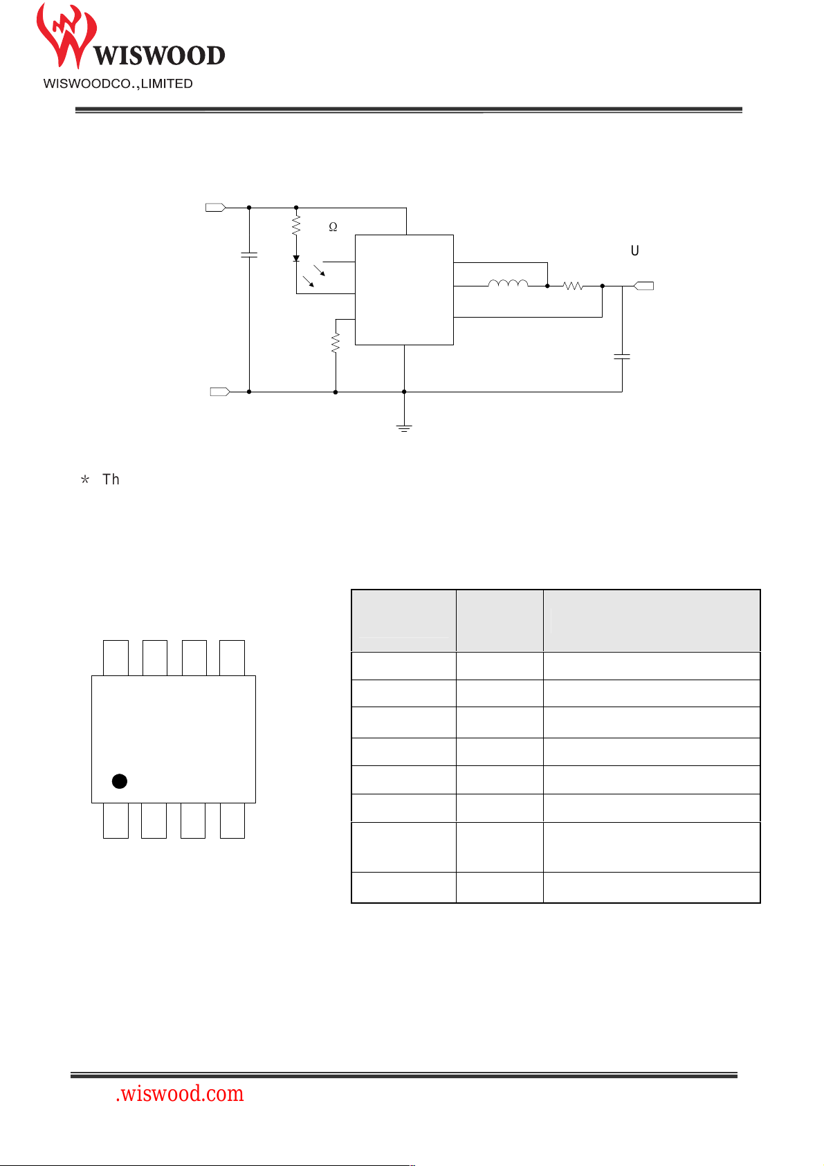
HHXX6622002
2
C1
R1 300
R2
10K
Ω
1
EN
7
CHRG
8
TS FB
= 0.17V/R3.
OUT1
TTyyppiiccaall AApppplliiccaattiioonn
*
The charge current can be set by I
DC+
10uF
GND
VIN
GND
6
PROG
SW
5
3
4
2
L1 4.7uH
R3
VOUT
Battery
C2
20uF
PPiinn AAssssiiggnnmmeenntt
8 7 6 5
Top View
TS CHRG VIN GND
1 2 3 4
EN FB PROG SW
SOP-8L
PIN
NUMBER
1 EN
2 FB
3 PROG Charge Current Program
4 SW
5 GND
6 VIN
7 CHRG
8 TS Temperature Sense
PIN NAME
FUNCTION
ON/OFF Control
Feedback
Switch Output
Ground
Input
Open-Drain Charge Status for
Output
2
Page 3
www.wiswood.com
HHXX6622002
2
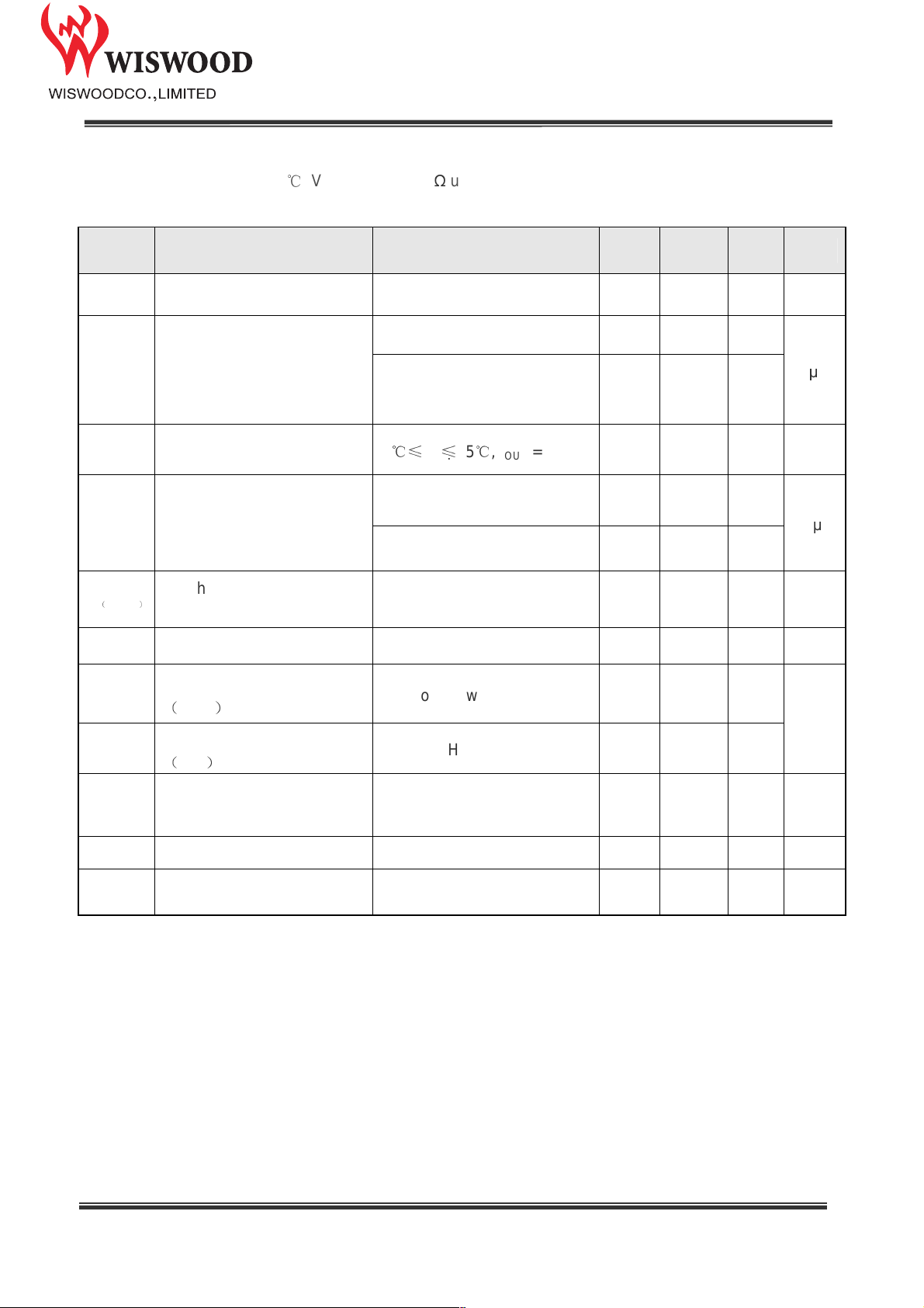
EElleeccttrriiccaall CChhaarraacctteerriissttiiccss
Operating Conditions: TA=25 , ℃VIN=5V, R3 = 0.1Ω unless otherwise specified.
SYMBOL
VIN Input Supply Voltage
IIN Input Supply Current
Regulated Output (Float)
Voltage
VOUT Pin Current
Precharge to fast-charge
)
transition threshold
V
V
I
(
FLOAT
OUT
LOWV
PARAMETER CONDITIONS MIN TYP MAX UNITS
Charge Mode
Standby Mode (Charge
Terminated)
0
℃≤
T
≤
85℃
, I
A
Standby Mode (Charge
Terminated), V
Shutdown Mode 4.3
Voltage on output pin 2.84 V
= 1.2A 4.15 4.2 4.24
OUT
= 4.2V
OUT
4.7 5.0 5.5 V
17
19.6
10.9
µ
A
V
µ
A
I
Trickle Charge Current V
TRIKL
V
TS-COLD
V
TS- HOT
I
TERM
VFB FB Pin Voltage Current Mode 0.17 V
f
OSC
TS Pin Threshold Voltage
(
Cold)
TS Pin Threshold Voltage
(
Hot)
Termination Current
Threshold
Switching Frequency 980 kHz
< V
BAT
VTS from Low to High
VTS from High to Low 0.5
202 mA
145 mA
TRIKL
2.5
V
3
Page 4
www.wiswood.com
HHXX6622002
2
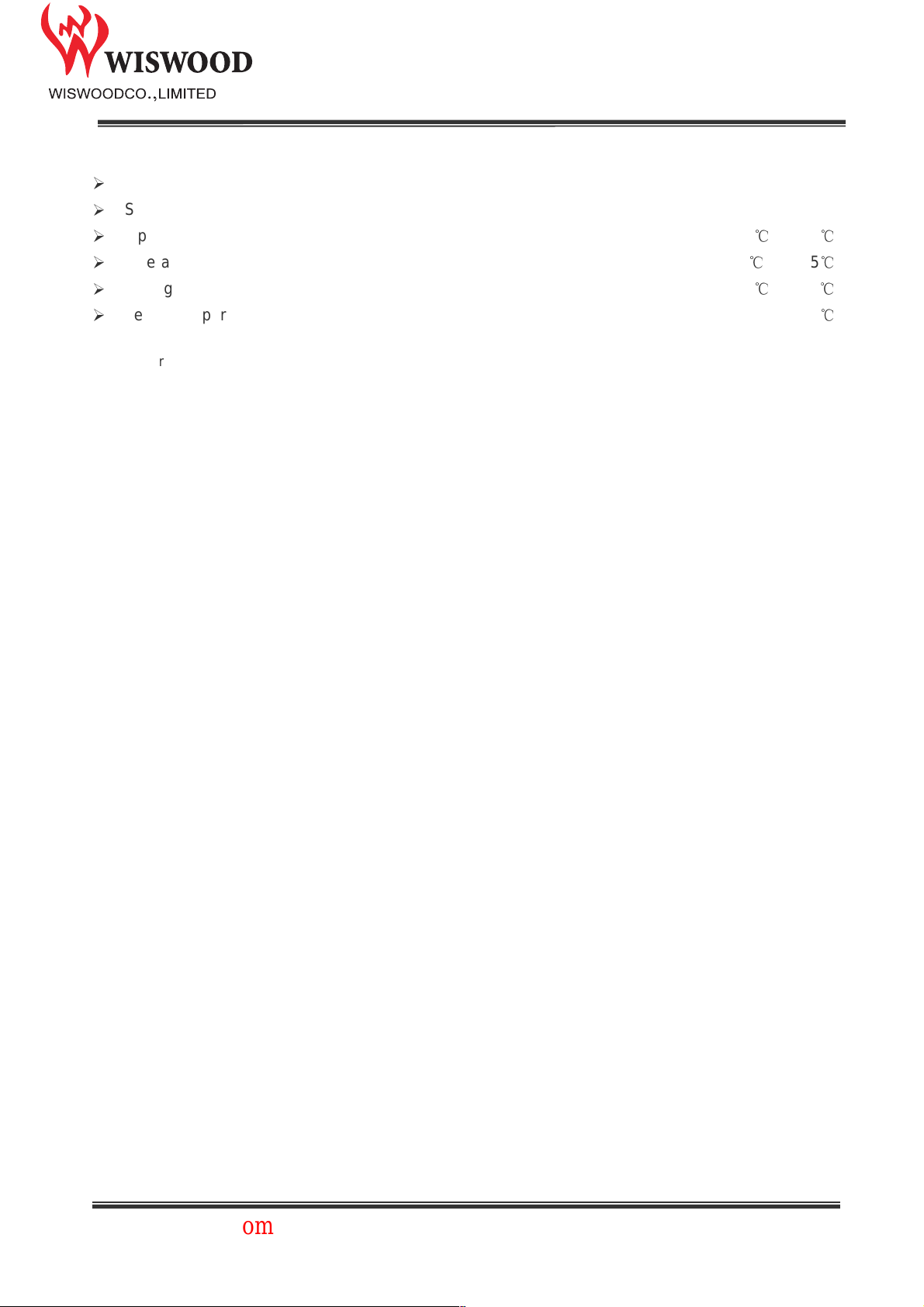
AAbbssoolluuttee MMaaxxiimmuumm RRaattiinnggs
VIN, CHRG, SW, PROG Voltage................................................................................. –0.3V to 6.5V
SW Pin Current ................................................................................................................ 3.8A
Operating Temperature Range (Note 2)............................................................... –40℃ to 85℃
Operating Junction Temperature (Note 3)................................................................. –40℃ to 125℃
Storage Temperature Range …………………………………………….................. –65 ℃to 125℃
Lead Temperature (Soldering, 10 sec)................................................................................. 300℃
Note 1: Stresses beyond those listed under Absolute Maximum Ratings may cause permanent damage to the device.
Exposure to any Absolute Maximum Rating condition for extended periods may affect device reliability and lifetime.
Note 2: The HX6202 is guaranteed to meet performance specifications from 0°C to 85°C. Specifications over the –40°C
to 85°C operating temperature range are assured by design, characterization and correlation with statistical process
controls.
Note 3: This IC includes over temperature protection that is intended to protect the device during momentary overload.
Junction temperature will exceed 125°C when over te mperature protection is active. Continuous operation above the
specified maximum operating junction temperature my impair device reliability.
s (Note 1)
4
Page 5
www.wiswood.com
HHXX6622002
2
PPiinn DDeessccrriippttiioonn
EN (Pin 1): ON/OFF Control(High Enable).
FB (Pin 2): Feedback Pin. Receives the feedback voltage from an external resistor across the output.
PROG (Pin 3): Charge Current Program. The output current is set by an external resistor according to
the following formula: I
SW (Pin 4): Charge Current Output. It provides charge current to the battery and regulates the final float
voltage to 4.2V. An internal precision resistor divider from this pin sets the float voltage which is
disconnected in shutdown mode.
GND (Pin 5): Ground.
VIN (Pin 6): Positive Input Supply Voltage. It Provides power to the charger VIN can range from 4.7V to
5V and should be bypassed with at least a 10uF capacitor.
CHRG (Pin 7): Open-Drain Charge Status Output. When the battery is charging, the CHRG pin is pulled
low by an internal N-channel MOSFET. When the charge cycle is completed or reverse battery lockout /
No AC is detected, CHRG is forced high impedance.
TS (Pin 8): Temperature Sense.
= 0.17V/R3.
OUT
5
Page 6
www.wiswood.com
HHXX6622002
2
OOppeerraattiioonn
The HX6202 is a constant current, constant voltage Li-Ion battery charger controller that uses a current
mode PWM step-down (buck) switching architecture. The charge current is set by an external sense
resistor (R3) across the PROG and FB pins. The final battery float voltage is internally set to 4.2V. For
batteries like lithium-ion that require accurate final float voltage, the internal reference, voltage amplifier
and the resistor divider provide regulation with high accuracy.
A charge cycle begins when the voltage at the VIN pin rises above the UVLO level and is 250mV or
greater than the battery voltage. At the beginning of the charge cycle, if the battery voltage is less than
the trickle charge threshold, the charger goes into trickle charge mode. The trickle charge current is
internally set to 9% of the full-scale current.
When the battery voltage exceeds the trickle charge threshold, the charger goes into the full-scale
constant current charge mode. In constant current mode, the charge current is set by the external sense
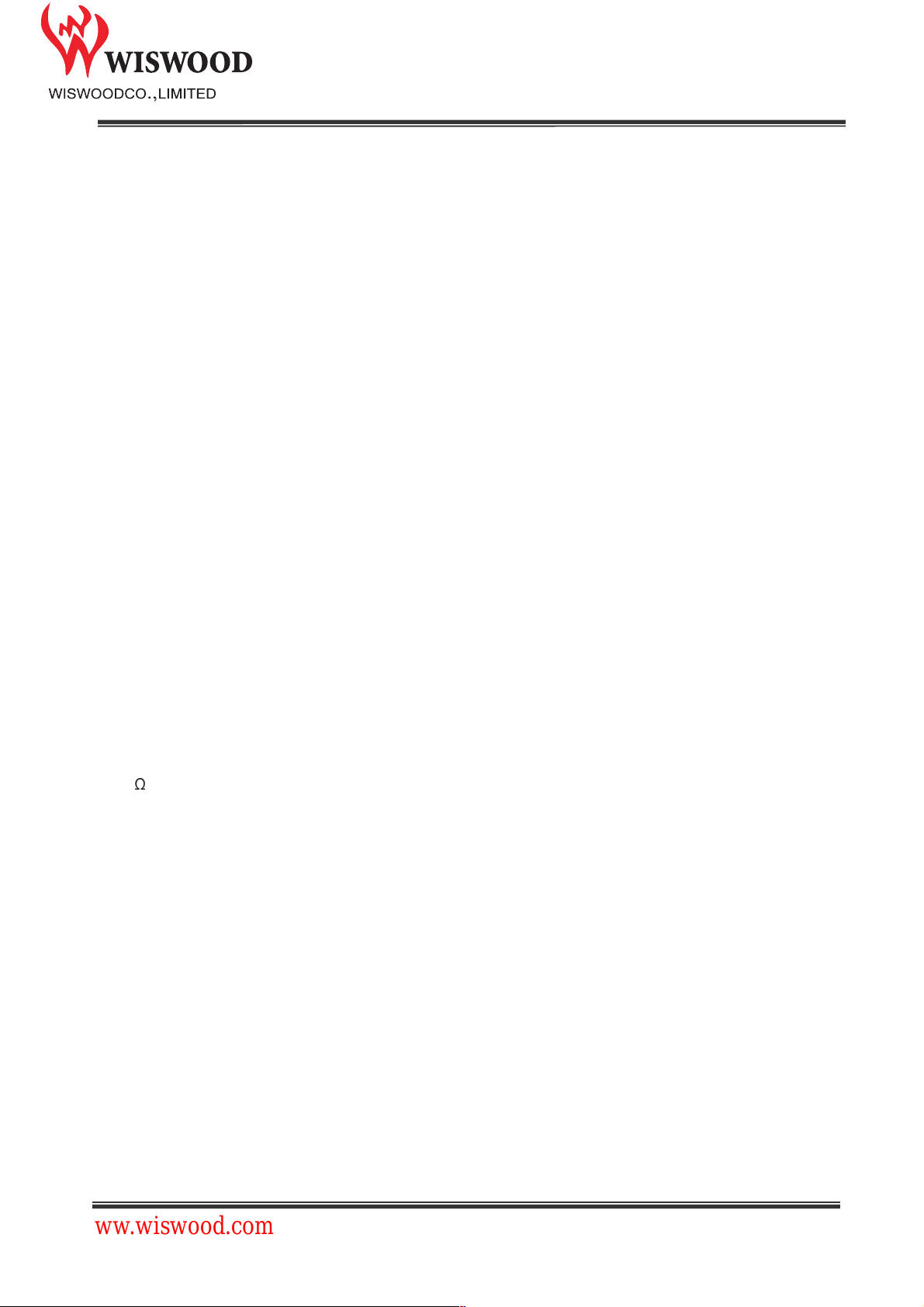
resistor R3 and an internal 170mV reference; I
When the battery voltage approaches the programmed float voltage, the charge current will start to
decrease. When the current drops to 15% of the full-scale charge current, an internal comparator turns
off the internal pull-down N-channel MOSFET at the CHRG pin, and connects a weak current source to
ground to indicate a end-of-charge condition and then the charge cycle is terminated and the CHRG pin
is forced high impedance.
= 170mV/R3.
OUT
To restart the charge cycle, remove and reapply the input voltage or momentarily shut the charger down.
Also, a new charge cycle will begin if the battery voltage drops below the recharge threshold voltage.
When the input voltage is present, the charger can be shut down. When the input voltage is not present,
the charger goes into sleep mode. This will greatly reduce the current drain on the battery and increase
the standby time.
A 10kΩ TS (negative temperature coefficient) thermistor can be connected from the TS pin to ground for
battery temperature qualification.
6
Page 7
www.wiswood.com
HHXX6622002
2
AApppplliiccaattiioonn IInnffoorrmmaattiioon
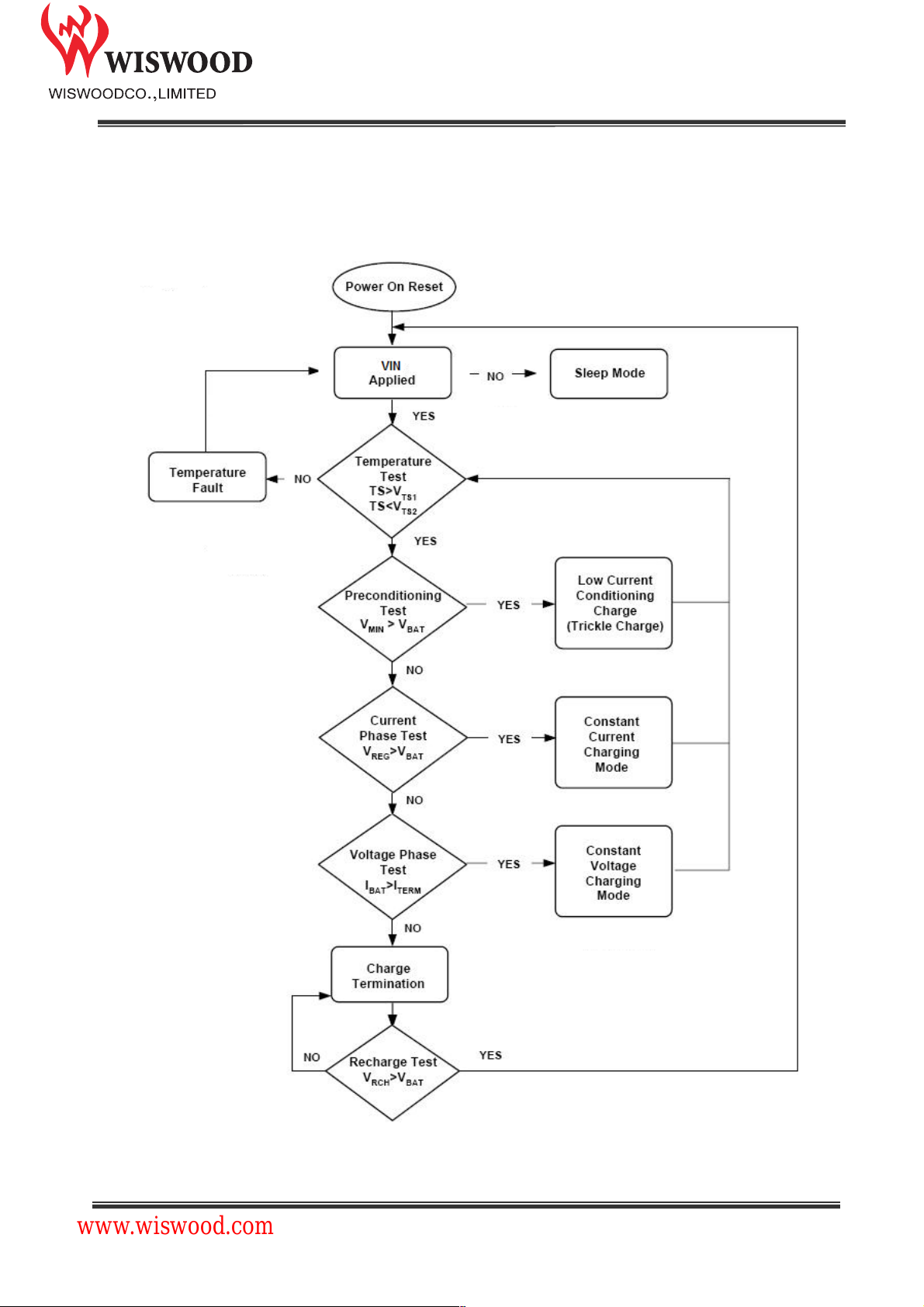
Functional Description
n
Figure 1: Operation Flow Chart
7
Page 8
www.wiswood.com
Qualification and Precharge
HHXX6622002
2
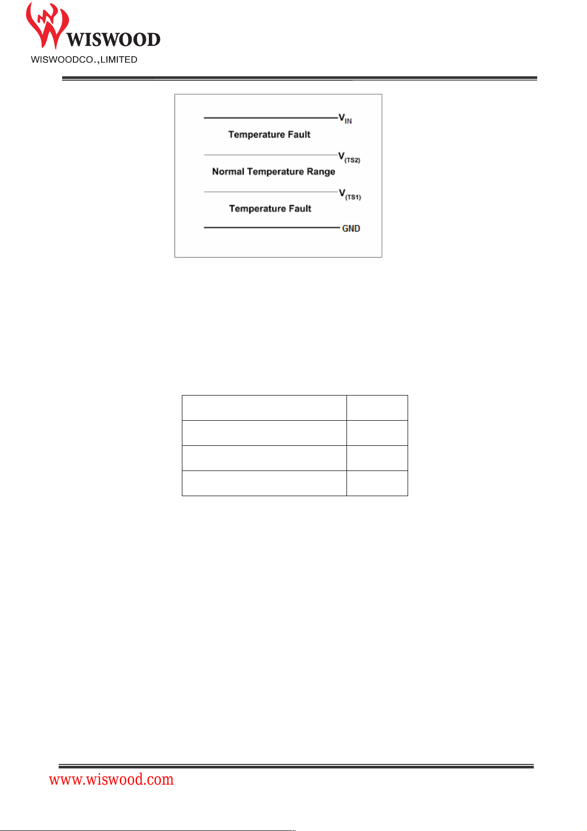
The HX6202 suspends charge if the battery temperature is outside the V
TS1
to V
range and suspends
TS2
charge until the battery temperature is within the allowed range. The HX6202 also checks the battery
voltage. If the battery voltage is below the precharge threshold V
condition the battery. The conditioning charge rate I
(PRECHG)
is set at approximately 8% of the regulation
, the HX6202 uses precharge to
(min)
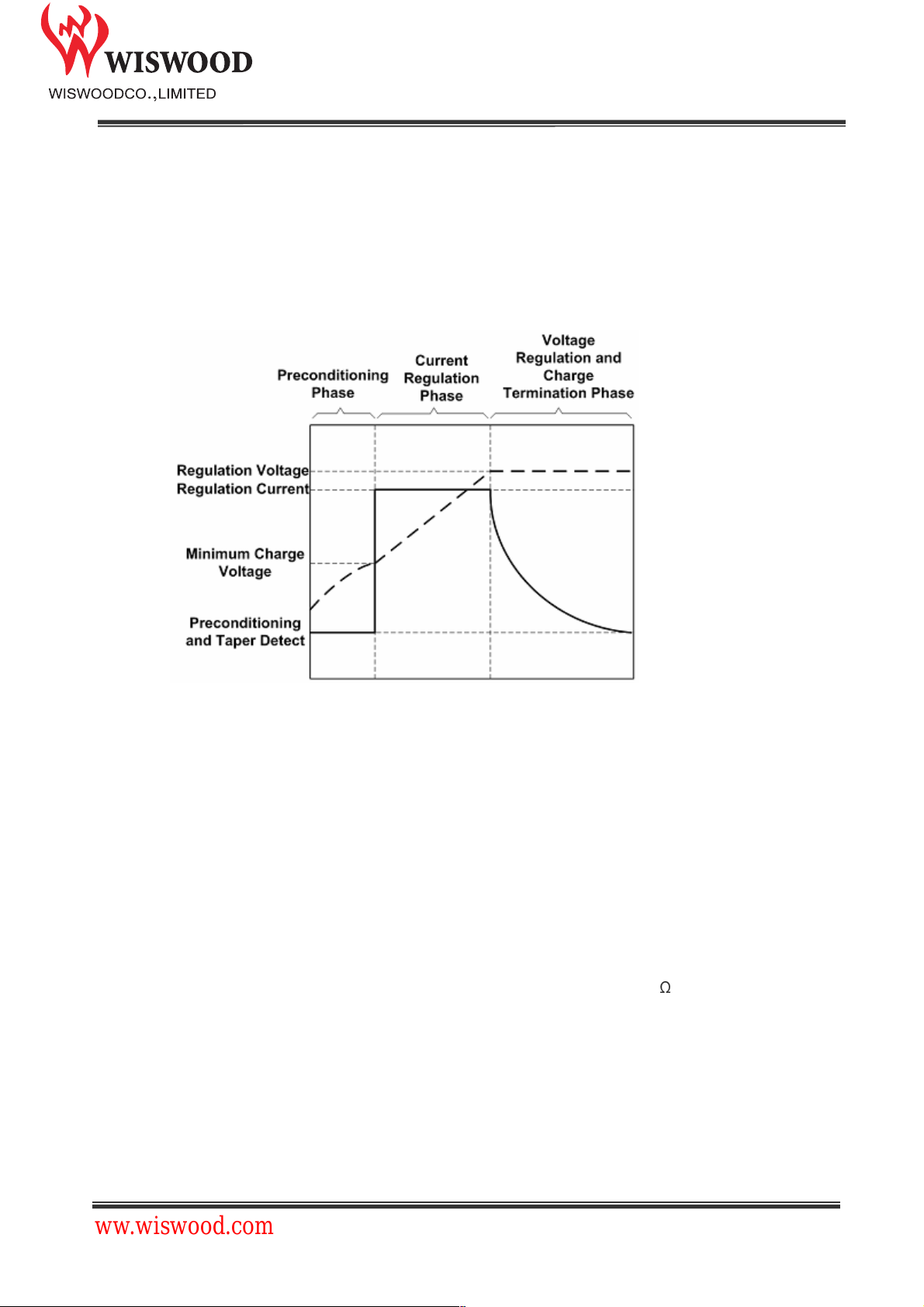
current. See Figure 2 for a typical charge-profile.
Figure 2: Typical Charge Profile
Charge Termination Recharge
The HX6202 monitors the charging current during the voltage-regulation phase. The HX6202 declares a
done condition and terminates charge when the current drops to the charge termination threshold, I
A new charge cycle begins when the battery voltage falls below the V
threshold.
RCH
TERM.
Battery Temperature Monitoring
The HX6202 continuously monitors temperature by measuring the voltage between the TS and GND
pin. An internal current source provides the bias for most common 10-kΩ negative-temperature
coefficient thermistors. The HX6202 compares this voltage against its internal V
TS1
and V
thresholds
TS2
to determine if charging is allowed (See Figure 3).
8
Page 9
www.wiswood.com
Charge Status Indication
Figure 3: TS Input Thresholds
HHXX6622002
2
The HX6202 reports the status of the charge on the CHRG pin. The following Table 1 summarized the
operation of the CHRG pin. The CHRG pin can be used to drive a chip LED.
Condition CHRG pin
Battery conditioning and charging Low
Charge complete(done) Hi-Z
Temperature fault or sleep mode Hi-Z
Table 1
Undervoltage Lockout (UVLO)
An undervoltage lockout circuit monitors the input voltage and keeps the charger off until VIN rises
above the UVLO threshold (4.2V ) and at least 250mV above the battery voltage. To prevent oscillation
around the threshold voltage, the UVLO circuit has 200mV per cell of built-in hysteresis. When
specifying minimum input voltage requirements, the voltage drop across the input blocking diode must
be added to the minimum supply voltage specification.
Trickle Charge
At the beginning of a charge cycle, if the battery voltage is below the trickle charge threshold, the
charger goes into trickle charge mode with the charge current reduced to 9% of the full-scale current.
9
Page 10
www.wiswood.com
Shutdown
The HX6202 can be shut down by pulling the EN pin to ground. In shutdown, the output of the CHRG
pin is high impedance and the quiescent current remains at 4.3uA.
Input and Output Capacitors
Since the input capacitor is assumed to absorb all input switching ripple current in the converter, it must
have an adequate ripple current rating. Worst-case RMS ripple current is approximately one-half of
output charge current. Actual capacitance value is not critical. Solid tantalum capacitors have a high
ripple current rating in a relatively small surface mount package, but caution must be used when
tantalum capacitors are used for input bypass. High input surge currents can be created when the
adapter is hot-plugged to the charger and solid tantalum capacitors have a known failure mechanism
when subjected to very high turn-on surge currents. Selecting the highest possible voltage rating on the
capacitor will minimize problems. Consult with the manufacturer before use. The selection of output
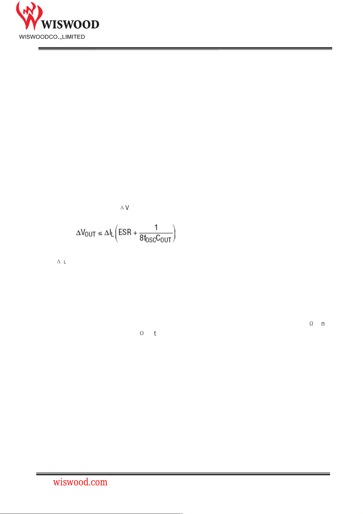
capacitor COUT is primarily determined by the ESR required to minimize ripple voltage and load step
transients. The output ripple
Δ
VOUT is approximately bounded by:
HHXX6622002
2
Since ΔIL increases with input voltage, the output ripple is highest at maximum input voltage. Typically,
once the ESR requirement is satisfied, the capacitance is adequate for filtering and has the necessary
RMS current rating.
Switching ripple current splits between the battery and the output capacitor depending on the ESR of
the output capacitor and the battery impedance. EMI considerations usually make it desirable to
minimize ripple current in the battery leads. Ferrite beads or an inductor may be added to increase
battery impedance at the 500kHz switching frequency. If the ESR of the output capacitor is 0.2
the battery impedance is raised to 4Ω with a bead or inductor, only 5% of the current ripple will flow in
the battery.
Ω
and
10
Page 11
www.wiswood.com
HHXX6622002
2
PPaacckkaaggiinngg IInnffoorrmmaattiioonn
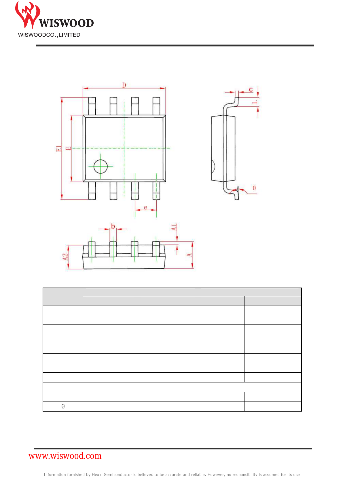
SOP-8L Package Outline Dimension
Symbol
A 1.350 1.750 0.053 0.069
A1 0.100 0.250 0.004 0.010
A2 1.350 1.550 0.053 0.061
b 0.330 0.510 0.013 0.020
c 0.170 0.250 0.006 0.010
D 4.700 5.100 0.185 0.200
E 3.800 4.000 0.150 0.157
E1 5.800 6.200 0.228 0.244
e 1.270(BSC) 0.050(BSC)
L 0.400 1.270 0.016 0.050
θ
0° 8° 0° 8°
Dimensions In Millimeters Dimensions In Inches
Min Max Min Max
Information furnished by Hexin Semiconductor is believed to be accurate and reliable. However, no responsibility is assumed for its use
11
d
Page 12

 Loading...