

Page 1

XRBH-1 User Manual
(V0.4)
Model Name: XRBH-1 BLE MODULE
Description: BLE module compatible
This document contains proprietary information which is the property of Wistron NeWeb
Corporation and is strictly confidential and shall not be disclosed to others in whole or in part,
reproduced, copied, or used as basic for design, manufacturing or sale of apparatus without the
written permission of Wistron NeWeb Corporation.
Page 2

1
Editio
n # Reason for revision
Issue date
V0.1
Initial Document (Draft version)
201
7/04/06
V0.3
Modify FCC Warning M
essage
2017/04/12
Revision History
V0.2 Add Module Dimension 2017/04/11
V0.4 Modify Max Transmit Power 2017/05/08
BLE module Delivery Specification V0.4
Page 3
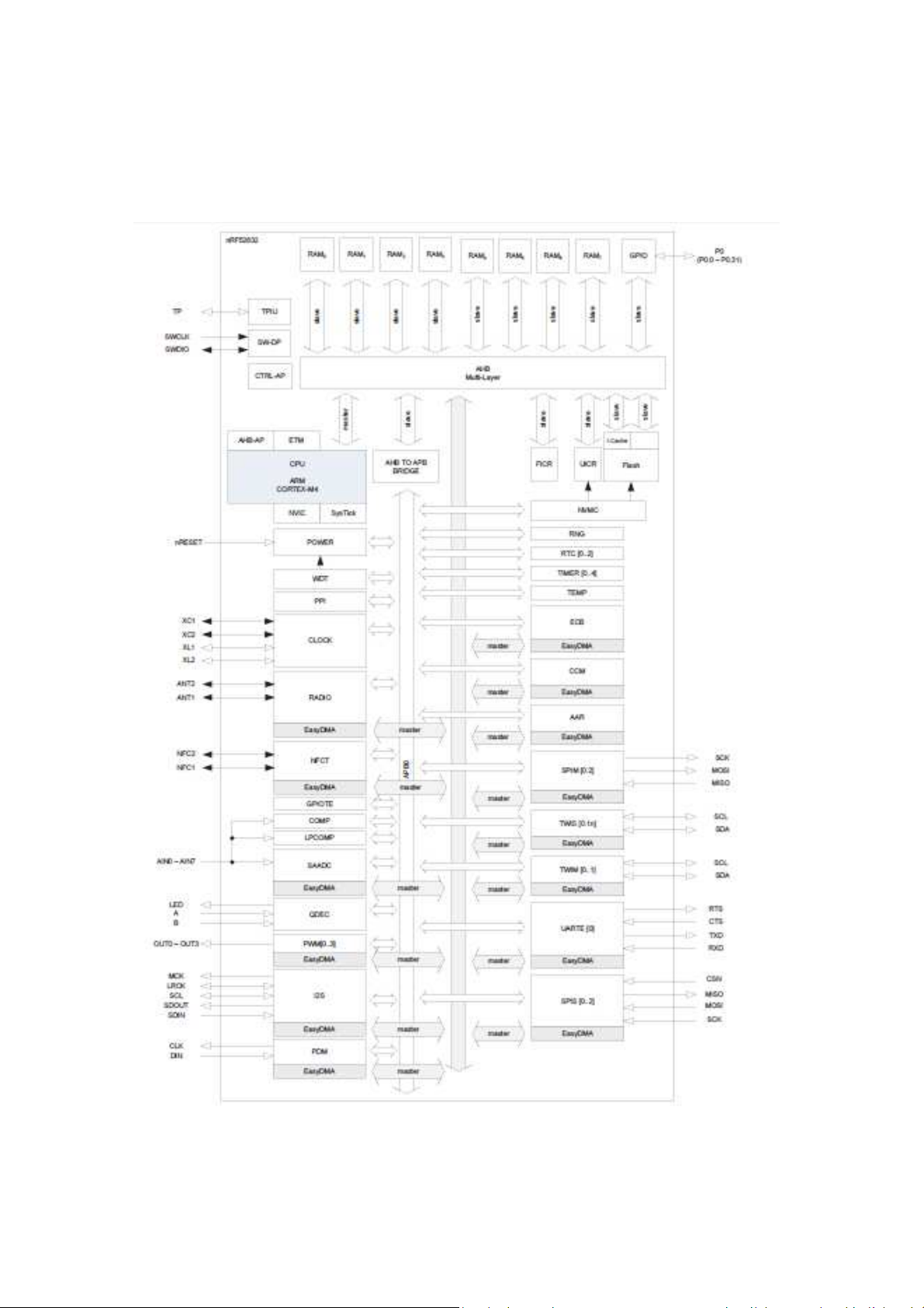
2
NRF52832 Block Diagram
1
BLE module Delivery Specification V0.4
Page 4
3
Specification
CATEGORIES
CATEGORIES FEATURE
CATEGORIESCATEGORIES
Bluetooth® V4.2 (Single Mode/Bluetooth Smart)
Frequency 2.402 - 2.480 GHz
FEATURE
FEATUREFEATURE
Wireless Specificiation
Host Interfaces
Encryption AES 128 bit using AES encryption
Memory
Max Transmit Power 4dBm +/- 1.0 dBm
Receive Sensitivity -96dBm (Low power mode)
Raw Data Rates 1 Mbps (over the air)
Total 30 lines – multi function
UART TX, RX
Default 115200, N, ,8, 1
From 1,200 to 115,200bps
GPIOs 30
SPI 3 lines
I2C 2 lines
ADC 8 lines (plus ADC reference)
Flash 512KB
RAM 64KB
Physical Dimensions 14mm x 9.8mm x 2.3mm
RF 32MHz crystal embedded
Clock Management
RTC 32.768KHz crystal embedded
Operating Temperature -10° to +65° C
Environmental
Storage Temperature -10 ˚C to +65 ˚C
Miscellaneous Lead Free Lead-free and RoHS compliant
BLE module Delivery Specification V0.4
Page 5
4
Electrical characteristics
DC/DC mode
Symbol Minimum Typical Maximum Unit
VCC 1.8 3 3.6 V
Power consumption
Symbol Description Typical Unit
I
OFF
I
IDLE
3V ON, all blocks idle 1.9 uA
System off current
consumption
0.7 uA
BLE module Delivery Specification V0.4
Page 6

5
Mechanical Dimension
BLE module Delivery Specification V0.4
Page 7

6
BLE module Delivery Specification V0.4
Page 8

7
Recommend Land Pattern
BLE module Delivery Specification V0.4
Page 9

8
PIN Define
Pin number Name Function Description
2 SWCLK Digital input
3 SWDIO Digital I/O
4 P0.21/RESET Digital I/O
5 P0.22 Digital I/O General purpose I/O pin.
6
7
TRACEDATA[0]
P0.20/
TRACECLK
P0.18/
Digital I/O
Digital I/O
Serial Wire Debug clock input for
debug and programming.
Serial Wire Debug I/O for debug and
programming.
General purpose I/O pin.
Configurable as pin reset.
General purpose I/O pin.
Trace port clock output.
General purpose I/O pin.
Trace port output.
Single Wire Output.
8 P0.19 Digital I/O General purpose I/O pin.
9 P0.17 Digital I/O General purpose I/O pin.
P0.16/
10
TRACEDATA[1]
11 P0.11 Digital I/O General purpose I/O pin
12 P0.13 Digital I/O General purpose I/O pin
P0.15/
13
TRACEDATA[2]
14 NFC2/P0.10
P0.14/
15
TRACEDATA[3]
16 P0.12 Digital I/O General purpose I/O pin
18 NFC1/P0.09
Digital I/O
Digital I/O
NFC input
Digital I/O
Digital I/O
NFC input
Digital I/O
General purpose I/O pin.
Trace port output.
General purpose I/O pin.
Trace port output.
NFC antenna connection.
General purpose I/O pin
General purpose I/O pin.
Trace port output.
NFC antenna connection.
General purpose I/O pin
20 P0.07 Digital I/O General purpose I/O pin
BLE module Delivery Specification V0.4
Page 10

9
22 P0.08 Digital I/O General purpose I/O pin
24 P0.06 Digital I/O General purpose I/O pin
Digital I/O
General purpose I/O pin
25 P0.04/AIN2
Analog input
Digital I/O
SAADC/COMP/LPCOMP input.
General purpose I/O pin.
26 P0.05/AIN3
Analog input
Digital I/O
SAADC/COMP/LPCOMP input.
General purpose I/O pin
27 P0.03/AIN1
Analog input
Digital I/O
SAADC/COMP/LPCOMP input.
General purpose I/O pin
29 P0.02/AIN0
Analog input
Digital I/O
SAADC/COMP/LPCOMP input.
General purpose I/O pin
31 P0.31/AIN7
Analog input
Digital I/O
SAADC/COMP/LPCOMP input.
General purpose I/O pin
32 P0.30/AIN6
Analog input
Digital I/O
SAADC/COMP/LPCOMP input.
General purpose I/O pin
33 P0.29/AIN5
Analog input
SAADC/COMP/LPCOMP input.
35 P0.26 Digital I/O General purpose I/O pin
36 P0.27 Digital I/O General purpose I/O pin
Digital I/O
General purpose I/O pin
37 P0.28/AIN4
Analog input
SAADC/COMP/LPCOMP input.
38 P0.25 Digital I/O General purpose I/O pin
39 P0.23 Digital I/O General purpose I/O pin.
40 P0.24 Digital I/O General purpose I/O pin.
1, 17, 19, 21, 23,
GND Ground Ground
34,41,42,43
28,30 VCC Power input +1.7V to +3.6V
BLE module Delivery Specification V0.4
Page 11

Antenna Type
Antenna Vendor WNC
Antenna Type PCB ANTENNA
Antenna Specification
BLE module Delivery Specification V0.4 10
Page 12

Test condition
BLE module Delivery Specification V0.4 11
Page 13

BLE module Delivery Specification V0.4 12
Page 14

(1)
(2)
FCC
FCC Label Compliance Statement:
This device complies with part 15 of the FCC Rules.
Operation is subject to the following two conditions:
(1) This device may not cause harmful interference, and
(2) This device must accept any interference received, including interference that
may cause undesired operation.
FEDERAL COMMUNICATIONS COMMISSION
INTERFERENCE STATEMENT:
This equipment has been tested and found to comply with the limits for
a Class B digital device, pursuant to part 15 of the FCC Rules. These
limits are designed to provide reasonable protection against harmful
interference in a residential installation.
This equipment generates, uses and can radiate radio frequency
energy and, if not installed and used in accordance with the
instructions, may cause harmful interference to radio
communications. However, there is no guarantee that interference will
not occur in a particular installation. If this equipment does cause
harmful interference to radio or television reception, which can be
determined by turning the equipment off and on, the user is
encouraged to try to correct the interference by one or more of the
following measures:
- Reorient or relocate the receiving antenna.
- Increase the separation between the equipment and receiver.
- Connect the equipment into an outlet on a circuit different from that
to which the receiver is connected.
- Consult the dealer or an experienced radio/ TV technician for help.
Compliance Statement
(3)
BLE module Delivery Specification V0.4 13
End Product Labeling:
The final end product must be labeled in a visible area with the
following:
ID can be used only when all FCC compliance requirements are met.
““““
Contains FCC ID: NKR-XRBH-1
””””
. The grantee's FCC
Page 15

(4)
Radiation Exposure Statement
This device is intended only for OEM integrators under the following
conditions:
1) this equipment complies with FCC radiation exposure limits set
forth for uncontrolled equipment and meets the FCC RF exposure
guidelines in Supplement C to DET 65 RF exposure rules. This
equipment has very low levels of RF energy that are deemed to comply
without testing of specific absorption ration (SAR), and
2) The transmitter module may not be co-located with any other
transmitter or antenna.
As long as 2 conditions above are met, further transmitter test will not
be required. However, the OEM integrator is still responsible for
testing their end-product for any additional compliance requirements
required with this module installed
IMPORTANT NOTE:
In the event that these conditions can not be met (for example certain
laptop configurations or co-location with another transmitter), then
the FCC authorization is no longer considered valid and the FCC ID
can not be used on the final product. In these circumstances, the OEM
integrator will be responsible for re-evaluating the end product
(including the transmitter) and obtaining a separate FCC
authorization.
(5)
Radiation Exposure Statement:
1) Any changes or modifications not expressly approved by the grantee
of this device could void the user's authority to operate the equipment.
2) This equipment complies with FCC radiation exposure limits set
forth for an uncontrolled environment.
(6) Manual Information To the End User:
The OEM integrator has to be aware not to provide information to the
end user regarding how to install or remove this RF module in the
user’s manual of the end product which integrates this module.
The end user manual shall include all required regulatory
information/warning as show in this manual
BLE module Delivery Specification V0.4 14
Page 16

本產品符合低功率電波輻射性電機管理辦法
第十二條
※經型式認證合格之低功率射頻電機,非經許可,公司、商號或使用者均不得擅自變更
頻率、加大功率或變更原設計之特性及功能。
第十四條
※低功率射頻電機之使用不得影響飛航安全及干擾合法通信;經發現有干擾現象時,應
立即停用,並改善至無干擾時方得繼續使用。
-
前項合法通信,指依電信法規定作業之無線電通信。
-
低功率射頻電機須忍受合法通信或工業、科學及醫療用電波輻射性電機設備之干擾。
此模組若安裝於其他平台時,該平台標籤需標明:
此平台內建無線模組
BLE module Delivery Specification V0.4 15
 Loading...