

Page 1

WirelessAudioModule
AVMD7520‐SWA3
ChrisO'Connor
2010/12/29
Customer P/N:
Avnera Model:
WNC P/N:
Description:
N/A
AVMD7520-SWA3
55SWA301.SG1
Wireless Audio Module
Page 2

AVMD7520-SWA3
W
+15dBm, integrated antenna, 4 channel digital I/O
ireless HD Audio Module Solution
General Description
The AVMD7520-SWA3 module is a
complete radio module solution
containing all the necessary HW and
FW to provide a system-integrationready, multichannel wireless HD audio
solution compatible with the AM2G and
AAL wireless audio system.
The module is comprised of an AV7520
IC combined with RF front-end circuits
(RF PA + balun + filter + RF switch),
FLASH memory, crystal, and passive
components. It is an FCC-certified
modular solution with high performance
PCB printed antennas. The module also
provides a convenient set of digital I/O
interfaces for digital audio through an
I2S port, host MCU control through an
SPI or I2C interface and optional GPIO
for various control and indicator
functions.
The module is a card slot style using the
36 pin PCIe card edge pin arrangement
to save space and cost in connecting to
a main system board.
Features
9 Complete, Integrated Wireless Module
o AV7520 IC
o Complete RF front-end
o Single +5V supply voltage connection
9 High Performance Audio and RF solution
o Supports 16 bit, 48kHz up to 24 bit, 96kHz digital
audio formats
o 120dB SNR Audio Path
o Fixed Low Latency solution
o +15dBm transmit RF output power
o -82dBm receive RF sensitivity
o Support for 30m/150m range NLOS/LOS
9 Digital interfaces and Audio
o 4 channel digital audio I/O (2 stereo I2S ports)
Configurable as input or output
o Stereo audio DAC output
o 4-wire SPI slave interface or 2-wire I2C-compatible
communication with the host MCU
9 Package and connections
o Compact size (38mm x 53mm)
o 36 pin (2x18) PCIe style card slot edge connector
o Dual PCB printed antennas for diversity support
CONTENTS SUBJECT TO CHANGE WITHOUT NOTICE 2 AVNERA PROPRIETARY & CONFIDENTIAL | PROVIDED UNDER NDA
Page 3

AVMD7520-SWA3 Module Datasheet – Preliminary revision 1.0
Revision History
Revision Change Summary Release Date
1.0 Initial release Nov, 2010
Table of Contents
General Description .............................................................................................................................................................. 2
Features ............................................................................................................................................................................... 2
List of Figures ....................................................................................................................................................................... 3
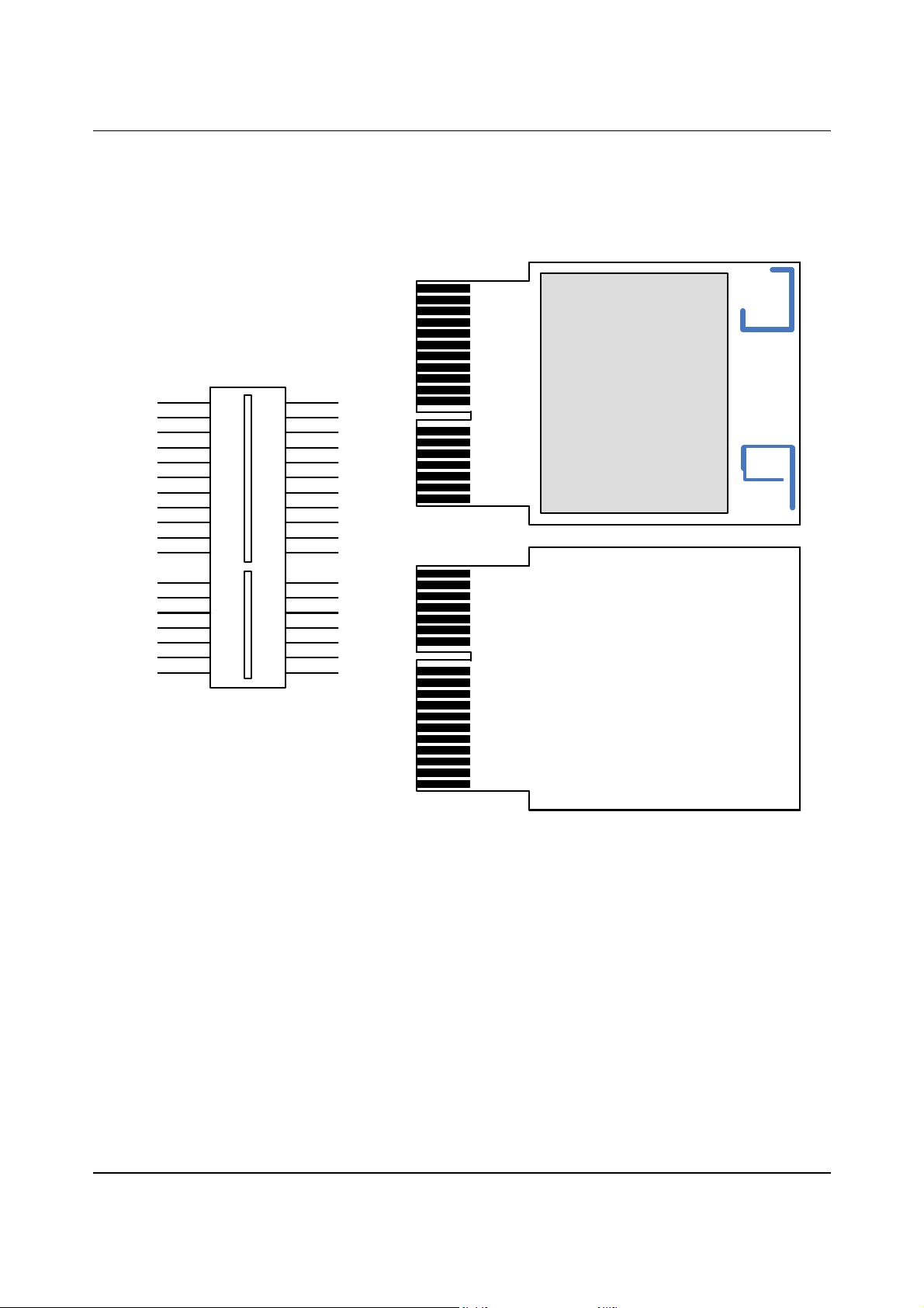
1 AVMD7520-SWA3 PIN CONFIGURATION................................................................................................................. 4
2 ELECTRICAL SPECIFICATIONS ............................................................................................................................... 6
2.1 Absolute Maximum Ratings ............................................................................................................................... 6
2.2 DC Electrical Characteristics ............................................................................................................................. 6
2.3 Electrical Characteristics – RF Receiver ............................................................................................................ 7
2.4 Electrical Characteristics – RF Transmitter ........................................................................................................ 7
2.5 Electrical Characteristics – RF Channel Frequency .......................................................................................... 8
2.6 Electrical Characteristics – End-to-end Audio Characteristics ........................................................................... 8
2.6.1 I2S Paths ...................................................................................................................................................... 8
2.6.2 Audio DAC Path ............................................................................................................................................ 8
2.7 Electrical Characteristics – MCLK Characteristics ............................................................................................. 9
2.8 Over-the-air Range ............................................................................................................................................ 9
3 Package Information ................................................................................................................................................. 10
3.1 Mechanical Dimensions ................................................................................................................................... 10
4 Ordering Information ................................................................................................................................................. 11
5 CONTACT INFO & LEGAL DISCLAIMER................................................................................................................. 12
FCC Statement ................................................................................................................................................................... 14
For product available in the USA/Canada market, only channel 1~11 can be operated. Selection of other channels is not
possible. ............................................................................................................................................... 錯誤! 尚未定義書籤。
IC Statement: ...................................................................................................................................................................... 16
List of Figures
Figure 1-1 – AVMD7520-SWA3 module pin configuration .................................................................................................... 4
Figure 3-1 - AVMD7520-SWA3 module mechanical dimensions ........................................................................................ 10
CONTENTS SUBJECT TO CHANGE WITHOUT NOTICE 3 AVNERA PROPRIETARY & CONFIDENTIAL | PROVIDED UNDER NDA
Page 4
AVMD7520-SWA3 Module Datasheet – Preliminary revision 1.0
1 AVMD7520-SWA3 PIN CONFIGURATION
B1
B2
B3
B4
B5
B6
B7
B8
B9
B10
B11
B12
B13
B14
B15
B16
B17
B18
A18
A17
A16
A15
A14
A13
A12
A11
A10
A9
A8
A7
A6
A5
A4
A3
A2
A1
B-side
(with shield can)
A-side
(No shield can)
VCCPA
VCC5V
ADAT3
BCLK3
WCLK3
MCLK_OUT
ADAT1
BCLK1
WCLK1
SDA
SCL
S_SSB
S_SCLK
S_MOSI
S_MISO
SRQ/PND
SM0
WM_DETN/GND
Connector
Top View
B1 A1
B2
B3
B4
B5
B6
B7
B8
B9
B10
B11
B12
B14
B15
B16
B17
B18
AVMD7520-SWA3
Pinout Configuration v.1
A2
A3
A4
A5
A6
A7
A8
A9
A10
A11
A12
A13B13
A14
A15
A16
A17
A18
GND
GND
GPIO2
GPIO23
GPIO22
GPIO18
GPIO17
GPIO16
GPIO7
GPIO6
GPIO4
GPIO3
GPIO5
GND
AGND
ROUT
LOUT
AGND
Figure 1-1 – AVMD7520-SWA3 module pin configuration
CONTENTS SUBJECT TO CHANGE WITHOUT NOTICE 4 AVNERA PROPRIETARY & CONFIDENTIAL | PROVIDED UNDER NDA
Page 5
AVMD7520-SWA3 Module Datasheet – Preliminary revision 1.0
Table 1-1 AVMD7520-SWA3 Pin Description
# Pin Name Pin Type Description
A1 GND Analog Module ground
A2 GND Analog Module ground
A3 GPIO2 Digital I/O GPIO #2 – See Note
A4 GPIO23 Digital I/O GPIO #23
A5 GPIO22 Digital I/O GPIO #22
A6 GPIO18 Digital I/O GPIO #18
A7 GPIO17 Digital I/O GPIO #17
A8 GPIO16 Digital I/O GPIO #16
A9 GPIO7 Digital I/O GPIO #7
A10 GPIO6 Digital I/O GPIO #6
A11 GPIO4 Digital I/O GPIO #4
A12 GPIO3 Digital I/O GPIO #3
A13 GPIO5 Digital I/O GPIO #5
A14 GND Ground Module ground – See Note
A15 AGND Analog Audio DAC ground; do not connect to module or system board ground
A16 ROUT Analog Audio DAC right channel output
A17 LOUT Analog Audio DAC left channel output
A18 AGND Analog Audio DAC ground; do not connect to module or system board ground
B1 VCCPA Analog +5V supply voltage input for the RF power amplifier
B2 VCC5V Analog +5V supply voltage input for the module
B3 ADAT3 Digital I/O I2S Audio Data for AV75xx I2S I/O Port # 3
B4 BCLK3 Digital I/O I2S Bit Clock for AV75xx I2S I/O Port # 3
B5 WCLK3 Digital I/O I2S Word Clock for AV75xx I2S I/O Port # 3
B6 MCLK_OUT Digital Output MCLK for I2S audio data
B7 ADAT1 Digital I/O I2S Audio Data for AV75xx I2S I/O Port # 1
B8 BCLK1 Digital I/O I2S Bit Clock for AV75xx I2S I/O Port # 1
B9 WCLK1 Digital I/O I2S Word Clock for AV75xx I2S I/O Port # 1
B10 SDA Digital I/O I2C compatible serial data I/O
B11 SCL Digital I/O I2C compatible serial clock I/O
B12 S_SSB Digital I/O SPI Slave – Slave Select (active low)
B13 S_SCLK Digital I/O SPI Slave – Serial Clock
B14 S_MOSI Digital I/O SPI Slave – Master Out / Slave In
B15 S_MISO Digital I/O SPI Slave – Master In / Slave Out
B16 SRQ/PND Digital Output Notification signal to host (pending notification)
B17 SM0 Digital Input Serial MUX control (for flash programming) and module reset (active low)
B18 WM_DETN / GND Digital output
Wireless module detect (low signal to indicate module is inserted in product) (This pin
is internally connected to “Module ground” pins A1, A2, & A14)
Note: The GPIO2 module pin assignment is different from that uses on the AVMD7520-SWA1 and AVMD7540-SWA4
modules, which assign GPIO2 to Pin A14
CONTENTS SUBJECT TO CHANGE WITHOUT NOTICE 5 AVNERA PROPRIETARY & CONFIDENTIAL | PROVIDED UNDER NDA
Page 6

AVMD7520-SWA3 Module Datasheet – Preliminary revision 1.0
2 ELECTRICAL SPECIFICATIONS
2.1 Absolute Maximum Ratings
The Absolute Maximum Rating (AMR) corresponds to the maximum value that can be applied without leading to
instantaneous or very short-term unrecoverable hard failure (destructive breakdown). Absolute Maximum Ratings are
stress ratings only. Permanent damage to the device may be caused by continuously operating at or beyond these limits.
Device functional operating limits and guaranteed performance specifications are given under Electrical Characteristics
and for the test conditions specified.
Table 2-1 AVMD7520-SWA3 Absolute Maximum Ratings
CONDITION MIN MAX Units
Supply (relative to GND)
+5V supply voltage range -0.3 6.0 V
Input Voltage Range – Digital Inputs -0.3 3.6V V
Short circuit to GND (any pin) --- continuous
Storage Temperature -20 +85 ºC
ESD Voltage Rating – Human Body Model test 2000 V
2.2 DC Electrical Characteristics
Operating Conditions: VCC = 5.0V ±10%, TA=0ºC to +50 ºC; RF Chan. Freq = 2412MHz to 2462MHz. All specifications are referenced to
the AVMD7520-SWA3 edge connector pins and RF connectors, unless otherwise specified. ““Typical”” specifications use VCC = 5.0V
and T
=25 ºC.
A
Table 2-2 AVMD7520-SWA3 DC Electrical Characteristics
PARAMETER CONDITIONS MIN TYP MAX UNIT
Input supply voltage Driven by an external regulator 4.5 5.5 V
Supply Current – +5V supply (Note 1) RESET 6 mA
OTA RX mode, 2 output channels via I2S 126 mA
OTA TX mode, 2 input channels via I2S 160 mA
FCC_TX (Pout = +15dBm) 425 mA
RX_search 220 mA
CMOS I/O Logic Levels – 3.3V I/O
Input Voltage Logic Low, VIL V
Input Voltage Logic High, VIH V
Output Voltage Logic Low, VOL V
Output Voltage Logic High, VOH V
Note 1: The operating states are defined as follows:
RESET: The AVMD7520-SWA2 is held in RESET by holding the SM0 input LOW
OTA-RX mode: The AVMD7520-SWA2 is operating in an Over-The-Air (OTA) link as a Client node, receiving 2 channels of
16bit, 48 kHz audio
OTA-TX mode: The AVMD7520-SWA2 is operating in an OTA link as an Arbiter node, transmitting 2 channels of 16bit 48 kHz
audio
FCC_TX mode: The AVMD7520-SWA2 is operating in the diagnostic “FCC_TX” mode
RX_search mode: The AVMD7520-SWA2 is configured as a Client and is powered ON but not operating in a link (in which
case it will be in continuous RX search mode)
= 3.3V 0.6 V
VDC33
= 3.3V 2.0 V
VDC33
VDC33
VDC33
= 3.3V; I
= 3.3V; I
=1mA 0.4 V
LOAD
=1mA 2.9 V
LOAD
CONTENTS SUBJECT TO CHANGE WITHOUT NOTICE 6 AVNERA PROPRIETARY & CONFIDENTIAL | PROVIDED UNDER NDA
Page 7

AVMD7520-SWA3 Module Datasheet – Preliminary revision 1.0
2.3 Electrical Characteristics – RF Receiver
Operating Conditions: VCC = 5.0V ±10%, TA=0ºC to +50 ºC; RF Chan. Freq = 2412MHz to 2462MHz. All specifications are referenced to
the AVMD7520-SWA3 edge connector pins and RF connectors, unless otherwise specified. ““Typical”” specifications use VCC = 5.0V
and T
=25 ºC.
A
Table 2-3 AVMD7520-SWA3 Electrical Characteristics – RF Receiver
PARAMETER CONDITIONS MIN TYP MAX UNIT
RF Channel Frequency Range 2412 2462 MHz
=25ºC
Sensitivity (Note 1)
Max Input Signal (Note 1)
Spurious RF outputs
LO leakage -47 dBm
Note 1: Sensitivity and max signal level are defined as the onset of 1% BLER Block Error Rate.
T
A
-5 dBm
2400-2483.5 MHz
<2400 MHz
>2483.5 MHz
-82 dBm
dBm
dBm
dBm
-47
-60
-60
2.4 Electrical Characteristics – RF Transmitter
Operating Conditions: VCC = 5.0V ±10%, TA=0ºC to +50 ºC; RF Chan. Freq = 2412MHz to 2462MHz. All specifications are referenced to
the AVMD7520-SWA3 edge connector pins and RF connectors, unless otherwise specified. ““Typical”” specifications use VCC = 5.0V
and T
=25 ºC.
A
Table 2-4 AVMD7520-SWA3 Electrical Characteristics – RF Transmitter
PARAMETER CONDITIONS MIN TYP MAX UNIT
RF Channel Frequency Range 2412 2462 MHz
Output Power (Note 1) TA=25ºC, OFDM signal, 16MHz channel BW +15 dBm
Harmonics (Note2) 2nd harmonic
Conducted RF Spurious signals (Note2)
Radiated Spurious RF signals (Note 3) 30-88MHz,
Note 1: Output power is the average transmitter output power in a 16MHz bandwidth centered on the channel, measured at the U.FL
connector with the port terminated into a load of 50 ohms at the frequency of interest. The stated specification refers to the
maximum level measured at either antenna port.
Note 2: Harmonic and Conducted RF Spurious Signal power are measured at the U.FL connector, with the port terminated into a load of
50 ohms at the frequency of interest. The stated specification refers to the maximum level measured at either antenna port.
Note 3: Radiated Spurious RF Signal strength is the radiated power measured in a calibrated chamber, with the module antenna ports
connected to dipole antennas having +2dBi (nominal) gain. The stated specification refers to the level measured from either
antenna port.
rd
3
harmonic
< 2390MHz; RBW=1MHz
> 2483.5MHz; RBW=1MHz
88-216MHz
216-960MHz
>960MHz
-50
-55
-45
-45
34
37
40
48
dBm
dBm
dBm
dBm
dBuV/m
dBuV/m
dBuV/m
dBuV/m
CONTENTS SUBJECT TO CHANGE WITHOUT NOTICE 7 AVNERA PROPRIETARY & CONFIDENTIAL | PROVIDED UNDER NDA
Page 8

AVMD7520-SWA3 Module Datasheet – Preliminary revision 1.0
2.5 Electrical Characteristics – RF Channel Frequency
Operating Conditions: VCC = 5.0V ±10%, TA=0ºC to +50 ºC; RF Chan. Freq = see below. All specifications are referenced to the
AVMD7520-SWA3 edge connector pins and RF connectors, unless otherwise specified. “Typical” specifications use VCC = 5.0V and
T
=25 ºC.
A
Table 2-5 AVMD7520-SWA3 Electrical Characteristics – RF Channel Frequencies
PARAMETER CONDITIONS MIN TYP MAX UNIT
AM2G system channel 1
Channel Frequency
Frequency Error 16MHz crystal +/- 20 ppm
AM2G system channel 2
AM2G system channel 3
2412
2438
2462
MHz
MHz
MHz
2.6 Electrical Characteristics – End-to-end Audio Characteristics
2.6.1 I2S Paths
Operating Conditions: VCC = 5.0V ±10%, TA=0ºC to +50 ºC; RF Chan. Freq = 2412MHz to 2462MHz. All specifications are referenced to
the AVMD7520-SWA3 edge connector pins and RF connectors, unless otherwise specified. “Typical” specifications use VCC = 5.0V and
T
=25 ºC.
A
Table 2-6 AVMD7520-SWA3 Electrical Characteristics – End-to-end Audio Characteristics
PARAMETER CONDITIONS MIN TYP MAX UNITS
End-to-end SNR I2S in to I2S out, no interference;
16bit / 48kHz mode
24bit / 48kHz mode
16bit / 96kHz mode
24bit / 96kHz mode
Latency 48kHz, interleaving level = 0
48kHz, interleaving level = 1
48kHz, interleaving level = 2
96kHz, interleaving level = 0
96kHz, interleaving level = 1
96kHz, interleaving level = 2
Bandwidth +/-0.5dB flatness, 48Khz modes
+/-0.5dB flatness, 96Khz modes
96
120
97
120
11
20
20
dB
dB
dB
dB
ms
15
19
9.5
13.5
17.5
20k
40k
ms
ms
ms
ms
ms
Hz
Hz
2.6.2 Audio DAC Path
Operating Conditions: VCC = 5.0V ±10%, TA=0ºC to +50 ºC; RF Chan. Freq = 2412MHz to 2462MHz. All specifications are referenced to
the AVMD7520-SWA2 edge connector pins and RF connectors, unless otherwise specified. Measurements use a 24bit, 96kHz digital I2S
audio input on the sending side. “Typical” specifications use VCC = 5.0V and T
=25 ºC.
A
Table 2-7 AVMD7520-SWA2 Electrical Characteristics – Analog Audio (DAC) Characteristics
PARAMETER CONDITIONS MIN TYP MAX UNITS
THD+N 0 dBFS -88 dB
Dynamic range fs = 48 kHz (-60 dBFS, A-weighted)
fs = 48 kHz (-60 dBFS, BW = 20Hz – 20kHz)
fs = 96 kHz (-60 dBFS, BW = 20Hz – 40kHz)
Channel isolation 100 dB
Load resistance 5 10 kΩ
Load capacitance 25 pF
CONTENTS SUBJECT TO CHANGE WITHOUT NOTICE 8 AVNERA PROPRIETARY & CONFIDENTIAL | PROVIDED UNDER NDA
99
99
99
dB
dB
dB
Page 9

AVMD7520-SWA3 Module Datasheet – Preliminary revision 1.0
Common-mode output voltage 1.40 V
Full-scale output voltage swing 1.70 V
p-p
Note: Audio DAC path characteristics reflect the capabilities of the on-chip DAC and module; however, care must be
taken in the layout and wiring of the external audio path to prevent degradation of the signal environment.
2.7 Electrical Characteristics – MCLK Characteristics
Operating Conditions: VCC = 5.0V ±10%, TA=0ºC to +50 ºC; RF Chan. Freq = 2412MHz to 2462MHz. All specifications are referenced to
the AVMD7520-SWA2 edge connector pins and RF connectors, unless otherwise specified. Measurements use a 24bit, 96kHz digital I2S
audio input on the sending side. “Typical” specifications use VCC = 5.0V and T
=25 ºC.
A
Table 2-8 AVMD7520-SWA3 Electrical Characteristics – MCLK Characteristics
PARAMETER CONDITIONS MIN TYP MAX UNITS
MCLK frequency
MCLK output duty cycle 40 60 %
“24MHz” mode (256MHz divide by 10.5)
“12MHz” mode (256MHz divide by 21)
24.38
12.19
MHz
MHz
2.8 Over-the-air Range
Operating Conditions: VCC = 5.0V ±10%, TA=0ºC to +50 ºC; RF Chan. Freq = 2412MHz to 2462MHz. All specifications are referenced to
the AVMD7520-SWA3 edge connector pins and RF connectors, unless otherwise specified. “Typical” specifications use VCC = 5.0V and
=25 ºC.
T
A
Table 2-9 AVMD7520-SWA3 Electrical Characteristics – Range
PARAMETER CONDITIONS MIN TYP MAX UNIT
LOS (line-of-sight) Range (Note 1) 2 channel audio link; >=100cm height 150 m
NLOS (non-line-of-sight) Range (Note 1)
Note 1: Range is defined as the maximum distance at which there are no audio breaks. The LOS environment is outdoors, with no
obstructions between the arbiter and client AV75xx radios. NLOS is indoors, with obstructions (typically walls) between the
arbiter and client AV75xx radios. NLOS range performance will be highly dependent on the actual environment.
2 channel audio link; >=100cm height
30 m
CONTENTS SUBJECT TO CHANGE WITHOUT NOTICE 9 AVNERA PROPRIETARY & CONFIDENTIAL | PROVIDED UNDER NDA
Page 10

AVMD7520-SWA3 Module Datasheet – Preliminary revision 1.0
3 Package Information
3.1 Mechanical Dimensions
3.0 mm
3.0 mm
4.6 mm
4.6 mm
45.60 mm
45.60 mm
57.50 mm
57.50 mm
1.60 mm
1.60 mm
8.50 mm
8.50 mm
8.85 mm
8.85 mm
20.05 mm
20.05 mm
21.95 mm
21.95 mm
29.15 mm
29.15 mm
38.00 mm
38.00 mm
Figure 3-1 - AVMD7520-SWA3 module mechanical dimensions
11.90 mm
11.90 mm
CONTENTS SUBJECT TO CHANGE WITHOUT NOTICE 10 AVNERA PROPRIETARY & CONFIDENTIAL | PROVIDED UNDER NDA
Page 11

AVMD7520-SWA3 Module Datasheet – Preliminary revision 1.0
4 Ordering Information
Table 4-1 AVMD7520-SWA3 Module Ordering Information
Module Part Number Description
AVMD7520-SWA3 +15dBm TX power, printed antenna, AV7520 based wireless audio module
CONTENTS SUBJECT TO CHANGE WITHOUT NOTICE 11 AVNERA PROPRIETARY & CONFIDENTIAL | PROVIDED UNDER NDA
Page 12

AVMD7520-SWA3 Module Datasheet – Preliminary revision 1.0
5 CONTACT INFO & LEGAL DISCLAIMER
Avnera Corporation
16505 Bethany Court, Suite 100
Beaverton, Oregon 97006
U.S.A.
Main: +1.503.718.4100
Fax: +1.503.718.4101
www.avnera.com
Avnera Corporation reserves the right to make changes without notice to the product to improve function, reliability, or
performance.
Avnera Corporation does not assume any liability arising from the application or use of the products or circuits described
herein.
CONTENTS SUBJECT TO CHANGE WITHOUT NOTICE 12 AVNERA PROPRIETARY & CONFIDENTIAL | PROVIDED UNDER NDA
Page 13

AVMD7520-SWA3 Module Datasheet – Preliminary revision 1.0
CONTENTS SUBJECT TO CHANGE WITHOUT NOTICE 13 AVNERA PROPRIETARY & CONFIDENTIAL | PROVIDED UNDER NDA
Page 14

AVMD7520-SWA3 Module Datasheet – Preliminary revision 1.0
FCC Statement
Federal Communication Commission Interference Statement
This equipment has been tested and found to comply with the limits for a Class B digital device, pursuant to Part 15 of the
FCC Rules. These limits are designed to provide reasonable protection against harmful interference in a residential
installation. This equipment generates, uses and can radiate radio frequency energy and, if not installed and used in
accordance with the instructions, may cause harmful interference to radio communications. However, there is no
guarantee that interference will not occur in a particular installation. If this equipment does cause harmful interference to
radio or television reception, which can be determined by turning the equipment off and on, the user is encouraged to try
to correct the interference by one of the following measures:
● Reorient or relocate the receiving antenna.
● Increase the separation between the equipment and receiver.
● Connect the equipment into an outlet on a circuit different from that to which the receiver is connected.
● Consult the dealer or an experienced radio/TV technician for help.
FCC Caution: Any changes or modifications not expressly approved by the party responsible
for compliance could void the user’s authority to operate this equipment.
This device complies with Part 15 of the FCC Rules. Operation is subject to the following two conditions: (1) This device
may not cause harmful interference, and (2) this device must accept any interference received, including interference that
may cause undesired operation.
This device and its antenna(s) must not be co-located or operation in conjunction with any other antenna or transmitter.
IMPORTANT NOTE:
FCC Radiation Exposure Statement:
This equipment complies with FCC radiation exposure limits set forth for an uncontrolled environment. This equipment
should be installed and operated with minimum distance 20cm between the radiator & your body.
CONTENTS SUBJECT TO CHANGE WITHOUT NOTICE 14 AVNERA PROPRIETARY & CONFIDENTIAL | PROVIDED UNDER NDA
Page 15

AVMD7520-SWA3 Module Datasheet – Preliminary revision 1.0
IMPORTANT NOTE:
This module is intended for OEM integrator. The OEM integrator is still responsible for the FCC compliance requirement
of the end product, which integrates this module.
20cm minimum distance has to be able to be maintained between the antenna and the users for the host this module is
integrated into. Under such configuration, the FCC radiation exposure limits set forth for an population/uncontrolled
environment can be satisfied.
Any changes or modifications not expressly approved by the manufacturer could void the user's authority to operate this
equipment.
USERS MANUAL OF THE END PRODUCT:
In the users manual of the end product, the end user has to be informed to keep at least 20cm separation with the
antenna while this end product is installed and operated. The end user has to be informed that the FCC radio-frequency
exposure guidelines for an uncontrolled environment can be satisfied. The end user has to also be informed that any
changes or modifications not expressly approved by the manufacturer could void the user's authority to operate this
equipment. If the size of the end product is smaller than 8x10cm, then additional FCC part 15.19 statement is required to
be available in the users manual: This device complies with Part 15 of FCC rules. Operation is subject to the following two
conditions: (1) this device may not cause harmful interference and (2) this device must accept any interference received,
including interference that may cause undesired operation.
LABEL OF THE END PRODUCT:
The final end product must be labeled in a visible area with the following " Contains TX FCC ID: NKR-SWA3". If the size
of the end product is larger than 8x10cm, then the following FCC part 15.19 statement has to also be available on the
label: This device complies with Part 15 of FCC rules. Operation is subject to the following two conditions: (1) this device
may not cause harmful interference and (2) this device must accept any interference received, including interference that
may cause undesired operation.
CONTENTS SUBJECT TO CHANGE WITHOUT NOTICE 15 AVNERA PROPRIETARY & CONFIDENTIAL | PROVIDED UNDER NDA
Page 16

AVMD7520-SWA3 Module Datasheet – Preliminary revision 1.0
IC Statement:
This Class B digital apparatus complies with Canadian ICES-003.
Cet appareil numérique de la classe B conforme á la norme NMB-003 du Canada.
This device complies with Industry Canada license-exempt RSS standard(s). Operation is subject to the following two
conditions: (1) this device may not cause interference, and (2) this device must accept any interference, including
interference that may cause undesired operation of the device.
Le présent appareil est conforme aux CNR d'Industrie Canada applicables aux appareils radio exempts de licence.
L'exploitation est autorisée aux deux conditions suivantes : (1) l'appareil ne doit pas produire de brouillage, et (2)
l'utilisateur de l'appareil doit accepter tout brouillage radioélectrique subi, même si le brouillage est susceptible d'en
compromettre le fonctionnement.
This device and its antenna(s) must not be co-located or operation in conjunction with any other antenna or transmitter.
IMPORTANT NOTE:
IC Radiation Exposure Statement:
This equipment complies with IC RSS-102 radiation exposure limits set forth for an uncontrolled environment. This
equipment should be installed and operated with minimum distance 20cm between the radiator & your body.
IMPORTANT NOTE:
This module is intended for OEM integrator. The OEM integrator is still responsible for the IC compliance requirement of
the end product, which integrates this module.
20cm minimum distance has to be able to be maintained between the antenna and the users for the host this module is
integrated into. Under such configuration, the IC RSS-102 radiation exposure limits set forth for an population/uncontrolled
environment can be satisfied.
Any changes or modifications not expressly approved by the manufacturer could void the user's authority to operate this
equipment.
USERS MANUAL OF THE END PRODUCT:
In the users manual of the end product, the end user has to be informed to keep at least 20cm separation with the
antenna while this end product is installed and operated. The end user has to be informed that the IC radio-frequency
exposure guidelines for an uncontrolled environment can be satisfied. The end user has to also be informed that any
changes or modifications not expressly approved by the manufacturer could void the user's authority to operate this
equipment. IC statement is required to be available in the users manual: This Class B digital apparatus complies with
Canadian ICES-003. Operation is subject to the following two conditions: (1) this device may not cause harmful
interference and (2) this device must accept any interference received, including interference that may cause undesired
operation.
LABEL OF THE END PRODUCT:
The final end product must be labeled in a visible area with the following " Contains TX IC : 4441A-SWA3 ".
CONTENTS SUBJECT TO CHANGE WITHOUT NOTICE 16 AVNERA PROPRIETARY & CONFIDENTIAL | PROVIDED UNDER NDA
 Loading...