

Page 1
AudioMagic™ AVMD6210-SWA12
AV6210
AVMD6210
AVMD6210
Preliminary Module Brief
Point-to-point AVMD6210-SWA12TX/RX modules for Stereo and Mono
Wireless Audio Systems, based on Avnera’s AV6210 IC
General Description
Every consumer wants to be free from wires,
but it has been challenging to find a low-cost,
high-quality, easy-to-use wireless audio
solution for the wireless subwoofer market.
Avnera’s proprietary wireless system takes a
new approach to wireless audio. The wireless
protocol was designed from the ground up and
delivers uncompressed mono or stereo audio,
with fixed latency and variable over the air
data rate support to eliminate interference
problems at the best possible audio quality.
Avnera’s wireless modules offer a low-touch,
easy-to-integrate wireless audio solution and
enable fast time to market by already solving
the problem associated with FCC certification,
antenna tuning and board optimization.
Modules based on Avnera’s AV6200 silicon
provide breakthrough wireless audio
functionality with fixed low-latency point-topoint transport of uncompressed mono PCM
audio data at up to 48KHz, 16-bit resolution
using digital (I2S) interfaces.
Applications
9 Wireless Subwoofers
9 Stereo audio channel transmission
Features
9 Audio Interfaces
9 I2S Digital Input Interface with 93dB
end-to-end digital audio path
9 Support for >15m range
9 Frequency range: 2.4 GHz ISM band,
continuous dynamic frequency selection
9 Forward error correction coding, error
detection, and audio-specific error
concealment
9 Custom Dual onboard printed PCB antennas
for multipath and fading mitigation
9 Auto-search/synch and dynamic channel
selection
9 Low, fixed latency of 16ms, suitable for
video lip-synch
9 Connector: 24 position 0.5mm flex cable
connector for maximum mounting flexibility
in the system.
9 Sample rate converter: Support for 16, 20,
24, and 32 bit PCM words at 8,16, 22.05,
24, 32, 44.1, and 48 kHz
9 General purpose over-the-air (OTA) serial
interface:
9 2 kbps, bi-directional, full duplex
9 Support for meta-data and remote
control commands
Ordering Options
AVMD6200-SWA12 TXD: Transmit module
with digital audio input and integrated printed
PCB antennas
AVMD6200-SWA12 RXD: Receive module
with digital audio output and integrated printed
PCB antennas
AVNERA CORPORATION | 16505 NW BETHANY COURT SUITE 100 | BEAVERTON, OREGON 97006, U.S.A. | MAIN +1.503.718.4100 | FAX +1.503.718.4101 | WWW.AVNERA.COM
AVNERA PROPRIETARY & CONFIDENTIAL | PROVIDED UNDER NDA
Page 2
AudioMagic AVMD6210-SWA12 Module Brief PRELIMINARY v0p1
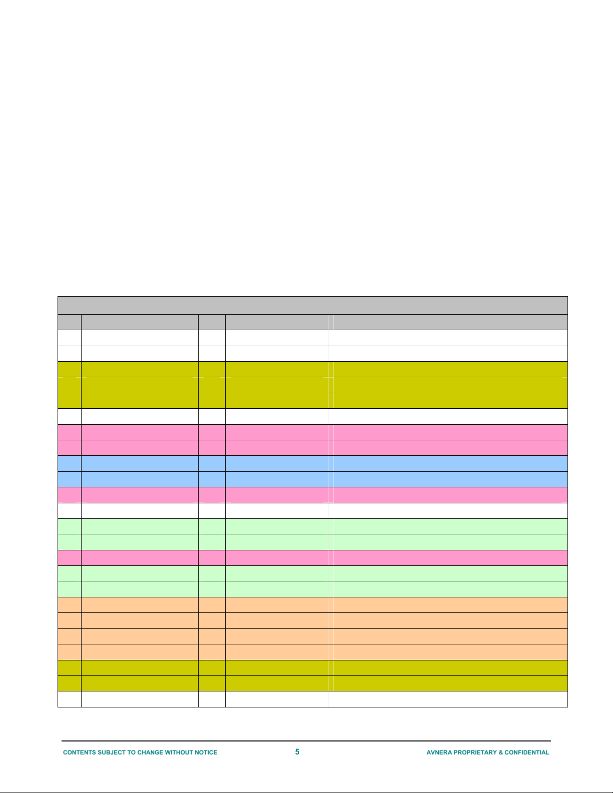
4 AVMD6210-SWA12- Connector Information
Table 1 shows the module connector pin out for the SWA12. A goal of the design is to have the e xact same pin out for
both the Tx and Rx modules. The module function is completely determined by firmware.
The module pins provide the capabilit y to use e ither SPI sl av e or I2C slav e interfac es – th ese are mutua ll y exclusiv e. If an
I2C slave host interface is used GPIOs 2 and 3 can be used for general purpose I/O. In addition, the SPI master port is
brought out to the connector to facilitate direct programmin g of the module flash memory if required. A single I2S port is
brought to the connector and can be configured to be either a slave or master port. The MCLK pin can be an input or
output to offer optimal flexibility. Likewise the I2S audio pin can be an input or output to implement either audio Tx or Rx.
In addition, there are 5 other GPIOs that can be used excl usively for s ystem features su ch as pair button, i nterrupt, LEDs
etc. The reset pin allows for an external device to reset the module but m ust be driven from an open dra in device to avoid
timing issues with the module reset.
Note: the connector pin out is subject to change throughout the development process to optimize the PCB
routing.
SWA12 Pin-Out
No Pin Name I/O AV6200 Pin Description
1 VDD - +5V +/- 10%
2 VDD - +5V +/- 10%
3 GPIO I/O GPIO13 pin 28 Function defined by firmware application.
4 GPIO I/O GPIO18 pin 43 Function defined by firmware application.
5 GPIO I/O GPIO19 pin 37 Function defined by firmware application.
6 Reset I Pin 24 Driven from open drain external source. Can be left open.
7 I2C_SCL_S / S_MISO I/O GPIO5 pin 44 I2C slave or SPI slave port
8 I2C_SDA_S / S_MOSI I/O GPIO4 pin 45 I2C slave or SPI slave port
9 I2C_SCL_M O GPIO22 pin 41 I2C master port or GPIO
10 I2C_SDA_M I/O GPIO21 pin 42 I2C master port or GPIO
11 S_SCLK I GPIO3 pin 46 SPI slave port or GPIO
12 GND - Ground
13 BCK1 I/O GPIO15 pin 26 I2S port
14 WCLK1 I/O GPIO16 pin 25 I2S port
15 S_SSB I GPIO2 pin 47 SPI slave port or GPIO
16 MCLK I/O GPIO10 pin 31 I2S port or GPIO
17 ADOUT/ADIN1 I/O GPIO14 pin 27 I2S port
18 M_SSB O GPIO6 pin 36 SPI master port
19 M_SCLK O GPIO7 pin 35 SPI master port
20 M_MOSI O GPIO8 pin 34 SPI master port
21 M_MISO I GPIO9 pin 33 SPI master port
22 GPIO I/O GPIO11 pin 30 Function defined by firmware application.
23 GPIO I/O GPIO12 pin 29 Function defined by firmware application.
24 GND - Ground
Table 1 – Rx and Tx SWA12 Module Pin-Out
CONTENTS SUBJECT TO CHANGE WITHOUT NOTICE 5 AVNERA PROPRIETARY & CONFIDENTIAL
Page 3
AudioMagic AVMD6210-SWA12 Module Brief PRELIMINARY v0p1
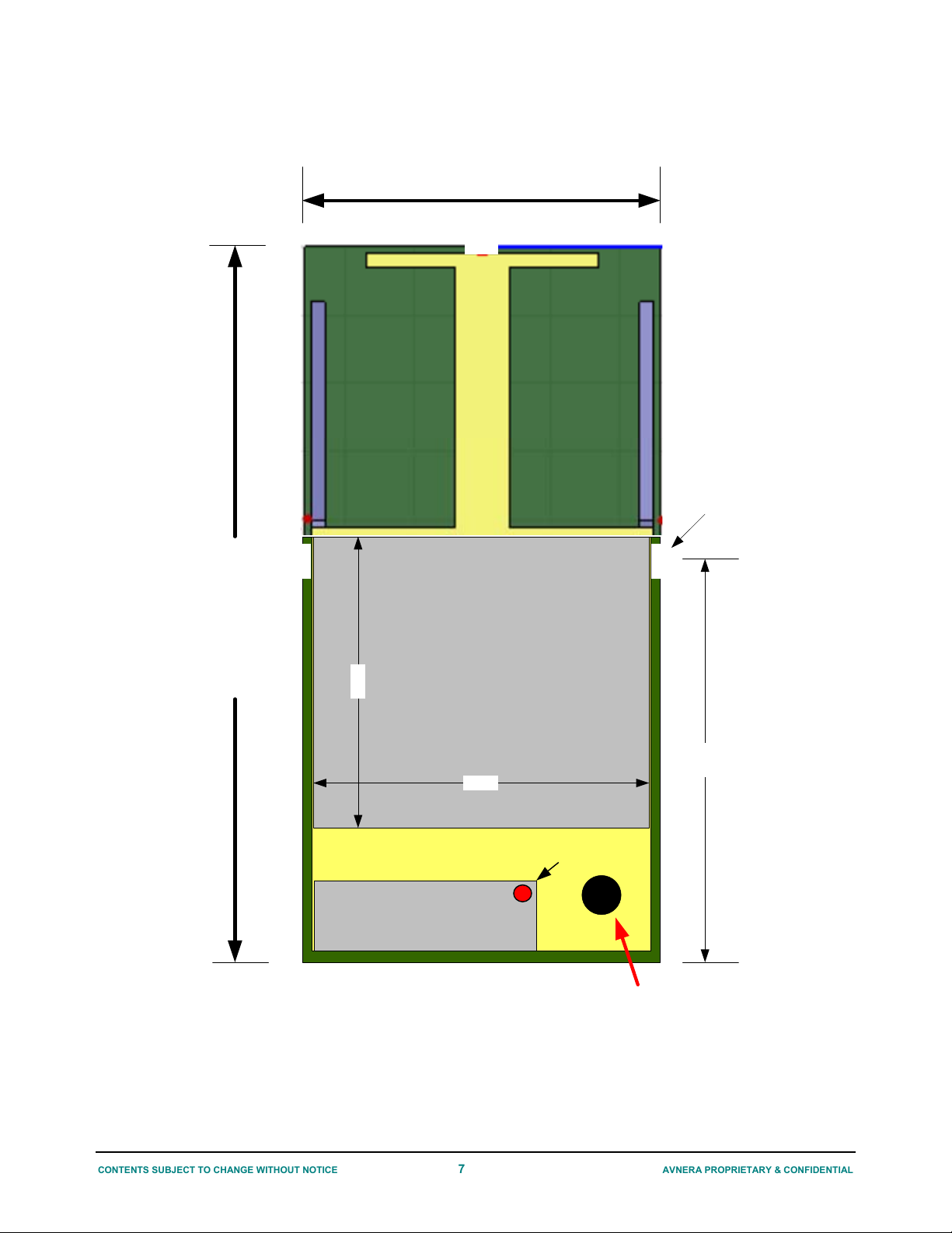
5 AVMD6210-SWA12 Mechanical Dimensions
26mm
1mm x 3mm
location slots
3 places
60mm
25mm
Shield Can
Approx 23 x 25mm
23mm
Pin 1
Connector
Mounting tabs
Mounting Hole
around perimeter
of PCB tbd
Figure 3 - AVMD6210-SWA12 mechanical dimensions
33mm
CONTENTS SUBJECT TO CHANGE WITHOUT NOTICE 7 AVNERA PROPRIETARY & CONFIDENTIAL
Page 4
AudioMagic AVMD6210-SWA12 Module Brief PRELIMINARY v0p1
6 Electrical Specifications
6.1 Absolute Maximum Ratings
Absolute Maximum Ratings (AMR) are stress ratings only. AMR corresponds to the maximum value that can be applied
without leading to instantaneous or very short-term unrecoverable hard fail ure (destructive breakdown). Stresses beyond
those listed under AMR may cause permanent damage to the device.
Functional operation of the device at these or any other conditions beyond those indicated under “Recommended
Operating Range” is not implied. Exposure to absolute-maximum-rated conditions for extended periods may adversely
affect device reliability.
Device functional operating limits and guaranteed performance sp ecifications are given under Electrical Char acteristics at
the test conditions specified.
CONDITION MIN MAX
VDD Supply Voltage Input -0.3V 6.0V
Input Voltage Range – Digital
1
Inputs
Operating Temperature -20ºC +80ºC
Storage Temperature -40ºC +100ºC
Assembly Temperature TBD
Static Discharge Voltage – HBM2 TBD
-0.3V 3.6V
Static Discharge Voltage – MM3 TBD
Notes:
Note 1: Digital GPIO Pins are 5V Tolerant when programmed as Inputs.
Note 2: Terminology: HBM => ESD human body model
Note 3: Terminology: MM => Machine model
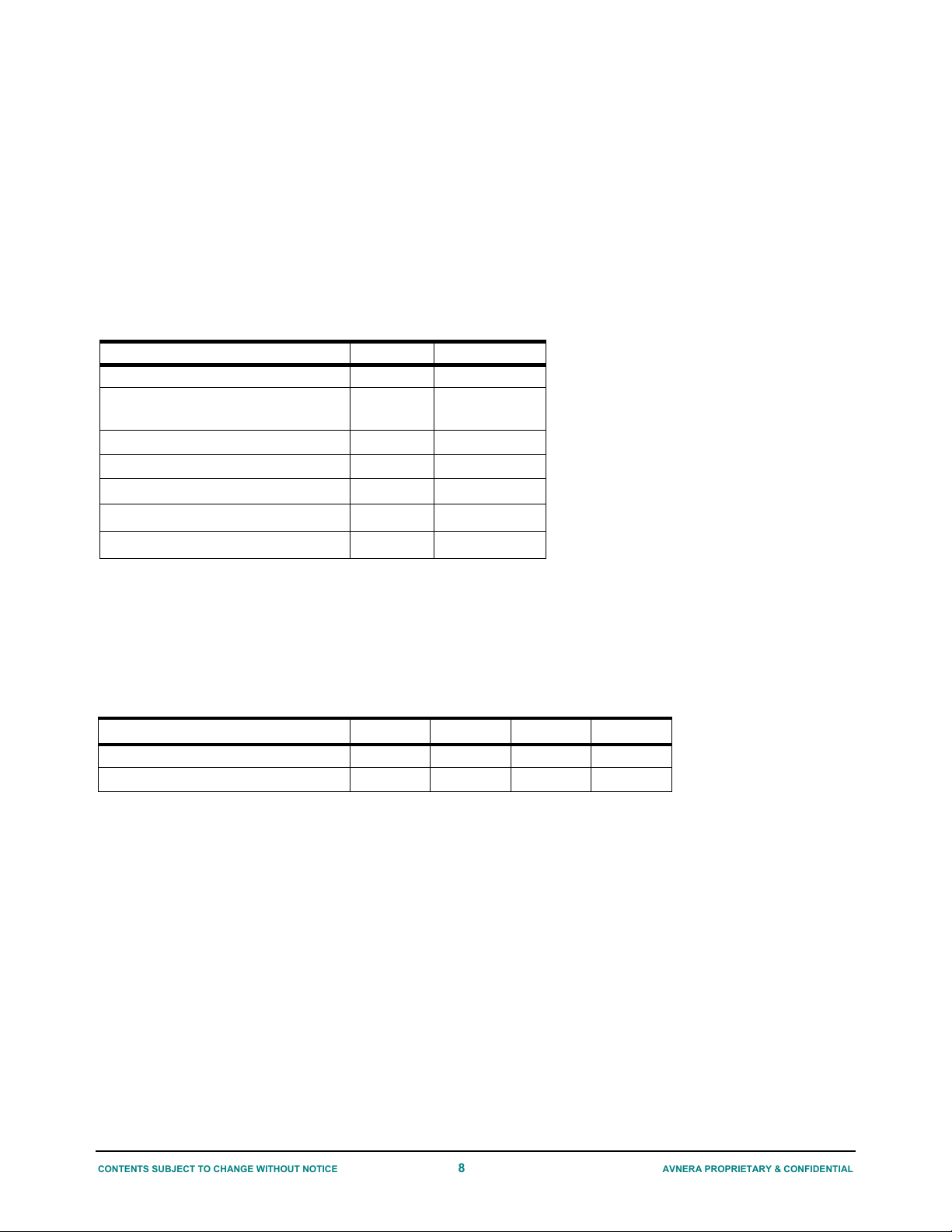
6.2 Recommended Operating Range
PARAMETER MIN TYP MAX UNIT
VDD Supply pin voltage 4.5 5.5 V
Ambient Temperature (TA) 0 70 ºC
CONTENTS SUBJECT TO CHANGE WITHOUT NOTICE 8 AVNERA PROPRIETARY & CONFIDENTIAL
Page 5

AudioMagic AVMD6210-SWA12 Module Brief PRELIMINARY v0p1
6.3 Electrical Characteristics
Test Conditions: TA=+25ºC, VDC=+5.0V
Table 2 - AVMD6210-SWA12 Electrical Characteristics
PARAMETER CO NDITIONS MIN TYP MAX UNIT
RF Frequency Range 2402 2478 MHz
RF Transmit power -3 0 dBm
RF Receiver sensitivity1 -86 -89 dBm
Range (LOS) >15 m
Audio SNR I2S Input/Output2 I2S end to end 16bit mode 90 93 dB
Audio SNR I2S Input/Output2 I2S end to end 12bit mode 70 72 dB
Analog Audio THD+N3 tbd dB
Audio Bandwidth (end to end I2S) 0.1dB point 20KHz mode 20 KHz
Audio Bandwidth (end to end I2S) 0.1 dB point 5KHz mode 5 KHz
Current consumption VDC(Active Audio mode) 50 mA
Note 1: AV6200 IC specification, measure by conducted u.fl connection at IC
Note 2: AVMD6200-SWA12-TX/RX
Note 3: Measured at -3dbFS input, A weighting. Output is taken, using external DAC on Avnera development board.
CONTENTS SUBJECT TO CHANGE WITHOUT NOTICE 9 AVNERA PROPRIETARY & CONFIDENTIAL
Page 6

AudioMagic AVMD6210-SWA12 Module Brief PRELIMINARY v0p1
7 Firmware Architecture
7.1 Standard Firmware Options
Avnera provides standard firmware images that implement basic wireless link operation. Each of these images uses 1
GPIO as a link status indicator and another GPIO is an input used to get the module into pairing mode as illustrated in
Figure 4.
Figure 4 – Standard Module Firmware Topology
The basic firmware image options supported are:
Tx Module Over-the-Air Audio Format I2S Configuration
SWA12TX-44/16-Slave 44KSps @ 16bit Stereo I2S Slave
SWA12TX-44/16-Master 44KSps @ 16bit Stereo I2S Master
SWA12TX-11/16-Slave 11KSps @ 16bit Mono I2S Slave
SWA12TX-11/16-Master 11KSps @ 16bit Mono I2S Master
Rx Module Over-the-Air Audio Format I2S Configuration
SWA12RX-44/16-Slave 44KSps @ 16bit Stereo I2S Slave
SWA12RX-44/16-Master 44KSps @ 16bit Stereo I2S Master
SWA12RX-11/16-Slave 11KSps @ 16bit Mono I2S Slave
SWA12RX-11/16-Master 11KSps @ 16bit Mono I2S Master
Table 3 – Standard Firmware Image Support
7.2 Custom Firmware Options
Beyond the basic audio, link status and pairing functionality, it is possible for Avnera to customize the firmware
functionality to support advanced system features such as over-the-air communic ation by means of either an I2C or SPI
host interface.
Customization may consist of features such as:
• Defined command and control API through I2C/SPI host interface
• Data transfer between the Tx and Rx modules
• Custom apps running on the module MCU to implement I2C master port or specific GPIO input/output functions
CONTENTS SUBJECT TO CHANGE WITHOUT NOTICE 10 AVNERA PROPRIETARY & CONFIDENTIAL
Page 7

AudioMagic AVMD6210-SWA12 Module Brief PRELIMINARY v0p1
7.3 Firm ware Upgrades
The possible interfaces that can be used for upgrades of the flash memory device are sh own in Figure 5.
With the standard firmware implementation, firmware upgrades are achieved by using the module SPI master port to
directly program the module flash device. Avnera provides a GUI application that runs on a PC to facilitate direct SPI
programming.
By means of additional custom firmware, programming of the module flash device can be achieved vi a the slave I2C or
SPI host interfaces.
It is also possible to implement over-the-air programming of the Rx module so all elements of a system can be upgr aded
through a single host interface. This requires working with customer to define the fu nctionality and architecture required as
well as the customer host interface and API to the Tx module.
SWA12 Module
Over the Air
Interface for Rx
Module
Avnera AV6210
Wireless
Transceiver
I2C Host
I/F
Custom Host
Figure 5 – Flash Programming Interface Options
SPI Host
Interfaces
8 Application information
8.1 Applica tion circuit
Application schematics are available from Avnera Support.
I/F
SPI
Master
Interface
Flash Memory
Device
Direct Flash
Progamming
CONTENTS SUBJECT TO CHANGE WITHOUT NOTICE 11 AVNERA PROPRIETARY & CONFIDENTIAL
Page 8

FCC Statement:
Federal Communication Commission Interference Statement
This equipment has been tested and found to comply with the limits for a Class B digital device,
pursuant to Part 15 of the FCC Rules. These limits are designed to provide reasonable protection
against harmful interference in a residential installation. This equipment generates, uses and can
radiate radio frequency energy and, if not installed and used in accordance with the instructions, may
cause harmful interference to radio communications. However, there is no guarantee that interference
will not occur in a particular installation. If this equipment does cause harmful interference to radio or
television reception, which can be determined by turning the equipment off and on, the user is
encouraged to try to correct the interference by one of the following measures:
● Reorient or relocate the receiving antenna.
● Increase the separation between the equipment and receiver.
● Connect the equipment into an outlet on a circuit different from that to which the receiver is
connected.
● Consult the dealer or an experienced radio/TV technician for help.
FCC Caution: Any changes or modifications not expressly approved by the party
responsible for compliance could void the user’s authority to operate this equipment.
This device complies with Part 15 of the FCC Rules. Operation is subject to the following two
conditions: (1) This device may not cause harmful interference, and (2) this device must accept any
interference received, including interference that may cause undesired operation.
This device and its antenna(s) must not be co-located or operation in conjunction with any other
antenna or transmitter.
IMPORTANT NOTE:
FCC Radiation Exposure Statement:
This equipment complies with FCC radiation exposure limits set forth for an uncontrolled environment.
This equipment should be installed and operated with minimum distance 20cm between the radiator &
your body.
Page 9

IMPORTANT NOTE:
This module is intended for OEM integrator. The OEM integrator is still responsible for the FCC
compliance requirement of the end product, which integrates this module.
20cm minimum distance has to be able to be maintained between the antenna and the users for the
host this module is integrated into. Under such configuration, the FCC radiation exposure limits set
forth for an population/uncontrolled environment can be satisfied.
Any changes or modifications not expressly approved by the manufacturer could void the user's
authority to operate this equipment.
USERS MANUAL OF THE END PRODUCT:
The end user has to be informed that the FCC radio-frequency exposure guidelines for an uncontrolled
environment can be satisfied. The end user has to also be informed that any changes or modifications
not expressly approved by the manufacturer could void the user's authority to operate this equipment.
If the size of the end product is smaller than 8x10cm, then additional FCC part 15.19 statement is
required to be available in the users manual: This device complies with Part 15 of FCC rules.
Operation is subject to the following two conditions: (1) this device may not cause harmful interference
and (2) this device must accept any interference received, including interference that may cause
undesired operation.
LABEL OF THE END PRODUCT:
The final end product must be labeled in a visible area with the following " Contains TX FCC ID:
NKR-SWA12 ". If the size of the end product is larger than 8x10cm, then the following FCC part 15.19
statement has to also be available on the label: This device complies with Part 15 of FCC rules.
Operation is subject to the following two conditions: (1) this device may not cause harmful interference
and (2) this device must accept any interference received, including interference that may cause
undesired operation.
Page 10

IC Statement:
This Class B digital apparatus complies with Canadian ICES-003.
Cet appareil numérique de la classe B conforme á la norme NMB-003 du Canada.
This device complies with Industry Canada license-exempt RSS standard(s). Operation is subject to
the following two conditions: (1) this device may not cause interference, and (2) this device must
accept any interference, including interference that may cause undesired operation of the device.
Le présent appareil est conforme aux CNR d'Industrie Canada applicables aux appareils radio exempts de licence.
L'exploitation est autorisée aux deux conditions suivantes : (1) l'appareil ne doit pas produire de brouillage, et (2)
l'utilisateur de l'appareil doit accepter tout brouillage radioélectrique subi, même si le brouillage est susceptible d'en
compromettre le fonctionnement.
This device and its antenna(s) must not be co-located or operation in conjunction with any other
antenna or transmitter.
IMPORTANT NOTE:
IC Radiation Exposure Statement:
This equipment complies with IC RSS-102 radiation exposure limits set forth for an uncontrolled
environment. This equipment should be installed and operated with minimum distance 20cm between
the radiator & your body.
Page 11

IMPORTANT NOTE:
This module is intended for OEM integrator. The OEM integrator is still responsible for the IC
compliance requirement of the end product, which integrates this module.
20cm minimum distance has to be able to be maintained between the antenna and the users for the
host this module is integrated into. Under such configuration, the IC RSS-102 radiation exposure limits
set forth for an population/uncontrolled environment can be satisfied.
Any changes or modifications not expressly approved by the manufacturer could void the user's
authority to operate this equipment.
USERS MANUAL OF THE END PRODUCT:
The end user has to be informed that the IC radio-frequency exposure guidelines for an uncontrolled
environment can be satisfied. The end user has to also be informed that any changes or modifications
not expressly approved by the manufacturer could void the user's authority to operate this equipment.
IC statement is required to be available in the users manual: This Class B digital apparatus complies
with Canadian ICES-003. Operation is subject to the following two conditions: (1) this device may not
cause harmful interference and (2) this device must accept any interference received, including
interference that may cause undesired operation.
LABEL OF THE END PRODUCT:
The final end product must be labeled in a visible area with the following " Contains TX IC :
4441A-SWA12 ".
 Loading...