

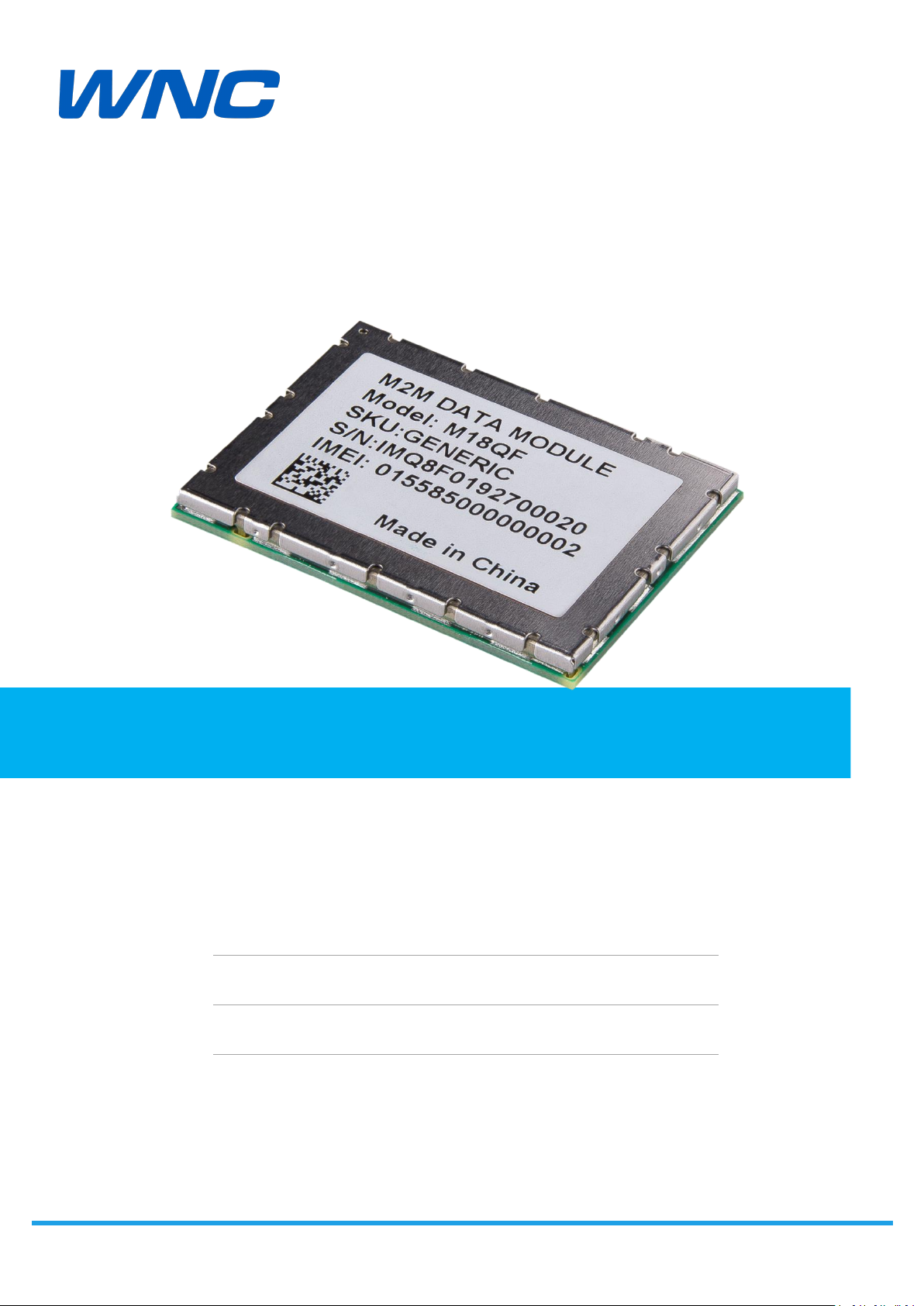
Wistron NeWeb M18QF Users manual
1/71
Product user manual
Project Name: M18QF&M18QA series
Author: Wistron NeWeb Corporation
Revision: 1.1
Revision Date: 2019/10/28

HW Design Guidelines
Contact Information
Technical Support website
https://SupportIoT.wnc.com.tw
Company Website
www.wnc.com.tw
Rev. #
Author
Summary of Changes
Date
1.0
WNC
First release
2019/8/12
1.1
WNC
Correct the band definition
2019/10/28
Revision History
2/71

HW Design Guidelines
© Wistron NeWeb Corporation
THIS DOCUMENT AND THE INFORMATION CONTAINED HEREIN IS PROPRIETARY AND IS THE
EXCLUSIVE PROPERTY OF WNC AND SHALL NOT BE DISTRIBUTED, REPRODUCED, OR
DISCLOSED IN WHOLE OR IN PART WITHOUT PRIOR WRITTEN PERMISSION FROM WNC.
LIMITATION OF LIABILITY
THIS DOCUMENT AND THE INFORMATION CONTAINED HEREIN IS PURELY FOR DESIGN
REFERENCE AND SUBJECT TO REVISION BY WNC AT ANY TIME. NOTHING IN THIS
DOCUMENT SHALL BE CONSTRUED AS GRANTING ANY WARRANTY OR RIGHT TO USE THE
MATERIAL CONTAINED HEREIN WITHOUT WNC’S PRIOR EXPRESS WRITTEN CONSENT. WNC
SHALL NOT BE LIABLE FOR ANY USE, APPLICATION OR DEVELOPMENT DERIVED FROM THE
MATERIAL WITHOUT SUCH PRIOR EXPRESS WRITTEN CONSENT.
3/71

HW Design Guidelines
Contents
Contact Information
Revision History
Contents
1. Introduction
2. Electrical Specifications
....................................................................................................................................
1.1. Abbreviation
1.2. Features
2.1. Host interface pin assignments
2.1.1. LGA Pad Diagram
2.1.2. Pin Assignments
2.2. Power supply
2.3. USB interface
2.4. SGMII interface
.................................................................................................................
........................................................................................................................
..........................................................................................................................
.............................................................................................................
....................................................................................................................
......................................................................................................
...........................................................................................................
..........................................................................................................
.......................................................................................................
...............................................................................
.........................................................................................
..........................................................................................
2
2
4
7
7
8
10
10
10
11
20
21
23
2.5. UIM interface
2.6. Control interface
2.6.1. Power-on Signal
2.6.2. Wake-up interface
2.6.3. Reset Signal
2.6.4. WWAN state Signal
2.7. Digital interface
2.7.1. JTAG Interface
2.7.2. SPI Master Interface
2.7.3. PCM Interface
2.7.4. I2S Interface
..........................................................................................................
.....................................................................................................
...........................................................................................
.......................................................................................
.................................................................................................
......................................................................................
.......................................................................................................
..............................................................................................
....................................................................................
..............................................................................................
................................................................................................
24
28
28
29
30
31
31
31
31
32
34
4/71

HW Design Guidelines
2.7.5. I2C Interface
................................................................................................
35
2.7.6. UART Interface
2.7.7. ADC Interface
3. RF Specifications
.................................................................................................................
3.1. RF connections
3.2. Interference and sensitivity
3.3. GNSS external circuit design
3.4. RF Specification
3.5.1 Band support
3.5.2 Bandwidth support
3.5.3 RF Transmit Specification
3.5.4 RF Receiver Specification
3.5.5 GNSS Receiver Specification
............................................................................................
..............................................................................................
........................................................................................................
....................................................................................
...................................................................................
.......................................................................................................
................................................................................................
......................................................................................
.............................................................................
.............................................................................
.........................................................................
36
36
37
37
38
39
41
41
42
42
42
44
4. Power
5. Software Interface
..................................................................................................................................
4.1. Power consumption
................................................................................................
..............................................................................................................
5.1. Support tools
5.2. USB interface
..........................................................................................................
..........................................................................................................
6. Mechanical and Environmental Certifications
6.1. PCBA Form Factor
6.2. Reflow
.....................................................................................................................
6.3. PCB pad design
6.4. Labeling
...................................................................................................................
6.5. SMT Voids control
6.5.1. Mother board PCB thickness
...................................................................................................
.......................................................................................................
...................................................................................................
.......................................................................
..................................................................
46
46
48
48
48
49
49
52
53
54
55
55
6.5.2. Stencil design
..............................................................................................
5/71
55

HW Design Guidelines
6.6. Thermal considerations
..........................................................................................
56
7. Regulatory Compliance and Certification
7.1. Certification testing
8. Packaging
............................................................................................................................
8.1. Tape-and-Reel Package
8.2. Single Packaging for Samples
8.3. MSL level
.................................................................................................................
9. Safety Recommendation
................................................................................................
...........................................................................................
..................................................................................
....................................................................................................
..........................................................................
58
58
59
59
61
61
62
6/71

HW Design Guidelines
1. Introduction
The M18QF/M18QA Series modules are LTE modems which incorporate an application CPU
1.1. Abbreviation
Table 1. Abbreviation
Abbreviation
Definition
AC
Alternating Current
DC
Direct Current
ETSI
European Telecommunications Standards Institute
GND
Ground
GPS
Global Positioning System
GNSS
Any single or combined satellite navigation system (GPS,
GLONASS and combined GPS/GLONASS)
GPIO
General Purpose Input Output
I/O
Input/Output
IoT
Internet of Things
I2C
Inter-Integrated Circuit
LGA
Land Grid Array
LTE
Long Term Evolution
Mbps
Megabits per second
MIPS
Millions of Instructions Per Second
N/A
Not/Applicable
OS
Operating System
PC
Personal Computer
PCM
Pulse Code Modulation
subsystem and peripheral interfaces and functions uniquely designed to address the
power/performance/cost requirements of IoT and M2M applications. The CPU is based on
Qualcomm’s MDM architecture which offers OFDMA-related software based signal
processing capabilities that significantly exceed traditional communications ARM cores.
M18QF/M18QA Series modules provide a variety of interfaces including USB 2.0, SGMII, SPI,
UART, PCM, I2C, UIM & SDIO.
7/71

HW Design Guidelines
PIN
Personal Identification Number
SIM
Subscriber Identity Module
SMA
Surface Mount Antenna
SPI
Serial Peripheral Interface
UART
Universal Asynchronous Receiver-Transmitter
UIM
User Identity Module
USB
Universal Serial Bus
Vref
Voltage reference
WCDMA
Wideband Code Division Multiple Access
WNC
Wistron NeWeb Corporation
1.2. Features
This section lists main features of M18QF/M18QA Series module support. For wireless
Table 2. M18QF/M18QA Series module overview
Module
Category
LTE
B2/5/4/12/13
LTE
B2/5/4/12/14
WCDMA
B2/5
GNSS
Temperature Grade
M18QF4√
×
√
√
Optional
Industrial
M14QF1√
×
√
√
Optional
Industrial
M18QA
4×√
√×Industrial
M14QA
1×√
√×Industrial
technology and band support information among different modules, please refer to table2
for detail information.
Note: 1.Refer to section6.6 for more information about industrial grade.
2.“√” indicates supporting. “×” indicates not supporting.
3. The 2nd harmonic of LTE B14 is not isolated completely from embedded GNSS
receiver, the interference would make GNSS de-sense seriously when LTE B14 and GNSS are
working simultaneously, the external GNSS receiver is recommended to use instead of
embedded GNSS in M18QA/M14QA.
8/71

HW Design Guidelines
Feature list:
LTE 3GPP release 10 without Carrier Aggregation
M18QF/M18QA: 3GPP, LTE Cat. 4 with 150/50 Mbps for DL/UL
M14QF/M14QA: 3GPP, LTE Cat. 1 with 10/5 Mbps for DL/UL
Supports LTE B2/4/5/12/13/14
Supports WCDMA B2/5, 3GPP release 8
Ultra-high-performance Cortex A7 microprocessor
Modem subsystem (MSS)
Resource and power management (RPM) subsystem
Optimized for M2M and IoT markets
Interfaces
–
HS USB 2.0 with integrated PHY
–
SGMII interface
–
Dual UART interfaces (4 bit and 2 bit) for data transfer and diagnostic tools
–
SDC1/First SPI interface
–
I2C/Second SPI interface
–
USIM interface
–
GPIOs
–
ADC
–
PCM/I2S
–
JTAG interface
9/71

HW Design Guidelines
2. Electrical Specifications
2.1. Host interface pin assignments
2.1.1. LGA Pad Diagram
Figure 1. LGA pad diagram (top view)
10/71

HW Design Guidelines
2.1.2. Pin Assignments
I/O type description:
AO : Analog Output
AI : Analog Input
DO : Digital Output
DI : Digital Input
Table 3. Pin interface family
Interface Family
Signal
Description
I/O
RF Interfaces
RF_2
Diversity antenna
AI
RF_GNSS
Reserved for GNSS receiver
AI
RF_1
Main Antenna
AI/AO
User Identity Module
UIM_VCC
Power source for UIM
AO
UIM_DATA
Data in/out
DI/DO
UIM_CLK
Clock signal
DO
UIM_RESET
Reset signal
DO
UIM_DETECT
UIM Detect signal
DI/DO
Data Interfaces- USB 2.0
USB_HS_DP
USB Data Positive
DI/DO
USB Detect
USB Detect
DI
USB_HS_DM
USB Data Negative
DI/DO
Data Interfaces- SGMII
SGMII_RX_P
SGMII receive - plus
DI
SGMII_RX_M
SGMII receive - minus
DI
SGMII_TX_P
SGMII transmit - plus
DO
SGMII_TX_M
SGMII transmit - minus
DO
SGMII_MDIO
SGMII Management data
DI/DO
SGMII_MDC
SGMII Management data clock
DI/DO
Data Interfaces- UART1
UART1_CTS_N
Clear To Send for UART 1
DI
UART1_RFR_N
Ready for receive for UART1
DO
11/71

12/71
HW Design Guidelines
UART1_RX
Receive for UART 1
DI
UART1_TX
Transmit for UART 1
DO
Data Interfaces- UART2
UART2_RX
Receive for UART 2
DI
UART2_TX
Transmit for UART 2
DO
Data Interfaces- I2C/2nd_ SPI
I2C_SDA
Data in/out
DI/DO
2nd_SPI_EN_1
2nd_SPI chip select
DO
I2C_SCL
Clock signal
DO
2nd_SPI_CLK
2nd_SPI serial clock
DO
SPI_MOSI
2nd_SPI master out slave in
DONCNC-SPI_MISO
2nd_SPI master in slave out
DI
Data Interfaces- SDC1/1st_SPI
SDC1_DATA_3
SDC1_DATA_3
DI/DO
1st_SPIM_MOSI
1st_SPI master out slave in
DO
SDC1_DATA_2
SDC1_DATA_2
DI/DO
1st_SPIM_MISO
1st_SPI master in slave out
DI
SDC1_DATA_1
SDC1_DATA_1
DI/DO
1st_SPIM_EN_1
1st_SPI chip select
DO
SDC1_DATA_0
SDC1_DATA_0
DI/DO
1st_SPIM_CLK
1st_SPI serial clock
DO
SDC1_CMD
SDC1_CMD
DI/DO
SDC1_CLK
SDC1_CLK
DO
Module Control and State Interfaces
WWAN_STATE
Wireless WAN Radio State
DO
POWER_ON
Power On the module
DI
WAKEUP_OUT
Module wakes up host
DO
WAKEUP_IN
Host wakes up module
DI
RESET
Reset the module
DI
Power and Ground
VREF
Voltage Reference Output
AO
VCC
Main Power
AI
GND
GND
AI
General Purpose
GPIO
Digital I/O
DI/DO

HW Design Guidelines
ADC_CONVENTOR
ADC_CONVENTOR
AI
AUDIO- PCM/I2S
PCM_DIN
PCM_DIN
DI
I2S_DATA0
I2S_DATA0
DI/DO
PCM_DOUT
PCM_DOUT
DO
I2S_DATA1
I2S_DATA1
DI/DO
PCM_CLK
PCM_CLK
DO
I2S_SCK
I2S_SCK
DO
PCM_SYNC
PCM_SYNC
DO
I2S_WS
I2S_WS
DO
RFU- RFU
RFU
Reserved For Future Use
-
Debug- JTAG
JTAG_SRST_N
JTAG reset for debug
DI
JTAG_TCK
JTAG clock input
DI
JTAG_TDI
JTAG data input
DI
JTAG_TDO
JTAG data output
DO
JTAG_TMS
JTAG mode select input
DI
JTAG_TRST_N
JTAG reset
DO
PS_HOLD
PS_HOLD
DI
Debug- Force_USB_BOOT
Force_USB_BOOT_CONFIG
Force USB BOOT CONFIG
DI
Table 4. Pin Assignments
Pin
No.
Modem mode
Host Mode
Voltage Level (V)
Min.
Typ.
Max.
1
GND
GND-0
-
2
GND
GND-0
-
3NCNC--
-
4
GND
GND-0
-
5
GND
GND-0
-
6
GND
GND-0
-
7
GND
GND-0
-
8
GND
GND-0
-
9
RF_GNSS
RF_GNSS--
-
10
GND
GND-0
-
13/71

14/71
HW Design Guidelines
11
GND
GND-0
-
12
GND
GND-0
-
13
GND
GND-0
-
14
GND
GND-0
-
15
RF_1
RF_1--
-
16
GND
GND-0
-
17
GND
GND-0
-
18
GND
GND-0
-
19
GND
GND-0
-
20
GND
GND-0
-
21
RF_2
RF_2--
-
22
GND
GND-0
-
23
GND
GND-0
-
24
GND
GND-0
-
25
GND
GND-0
-
26
GND
GND-0
-
27NCNC--
-
28
GND
GND-0
-
29
GND
GND-0
-
30
GND
GND-0
-
31
GND
GND-0
-
32
GND
GND-0
-
33NCNC--
-
34
GND
GND-0
-
35
GND
GND-0
-
36
GND
GND-0
-
37
VCC1
VCC1
3.3
3.8
4.2
38
VCC2
VCC2
3.3
3.8
4.2
39
VCC3
VCC3
3.3
3.8
4.2
40
VCC4
VCC4
3.3
3.8
4.2
41
VCC5
VCC5
3.3
3.8
4.2
42
VCC6
VCC6
3.3
3.8
4.2
43NCNC--
-
44
GND
GND-0
-
45
GND
GND-0
-
46
PCM_SYNC/GPIO46
PCM_SYNC/GPIO46
1.7
1.8
1.9

HW Design Guidelines
47
PCM_DIN/GPIO47
PCM_DIN/GPIO47
1.7
1.8
1.9
48
PCM_DOUT/GPIO48
PCM_DOUT/GPIO48
1.7
1.8
1.9
49
PCM_CLK/GPIO49
PCM_CLK/GPIO49
1.7
1.8
1.9
50
GND
GND-0
-
51
GND
GND-0
-
52
GPIO01/Force USB
BOOT Config
*8
GPIO01/Force USB
BOOT Config*
8
1.7
1.8
1.9
53
GPIO02
GPIO02
1.7
1.8
1.9
54
GPIO03
GPIO03
1.7
1.8
1.9
55
GPIO04
GPIO04
1.7
1.8
1.9
56NCSGMII_TX_P
-
Note5
-
57NCSGMII_TX_M
-
Note5
-
58NCSGMII_RX_P
-
Note5
-
59NCSGMII_RX_M
-
Note5
-
60
I2C_SDA
I2C_SDA/
2nd_SPI_EN_1
1.7
1.8
1.9
61
I2C_SCL
I2C_SCL/
2nd_SPI_CLK
1.7
1.8
1.9
62NC2nd_SPI_MOSI
1.7
1.8
1.9
63NC2nd_SPI_MISO
1.7
1.8
1.9
74
GND
GND-0
-
75
GND
GND-0
-
76
RFFE1_DATA
RFFE1_DATA
---
77
RFFE1_CLK
RFFE1_CLK
---
78NCNC--
-
79NCNC--
-
80
UART1_CTS (UART 1)
UART1_CTS (UART 1)
1.7
1.8
1.9
81
UART1_RTS (UART 1)
UART1_RTS (UART 1)
1.7
1.8
1.9
82
UART1_RX (UART 1)
UART1_RX (UART 1)
1.7
1.8
1.9
83
UART1_TX (UART 1)
UART1_TX (UART 1)
1.7
1.8
1.9
84
GND
GND-0
-
85
GND
GND-0
-
86
USB_Dp
USB_Dp
-
Note6
-
87
USB Detect
*7
USB Detect
*7
1.7
1.8
1.9
88
USB_Dn
USB_Dn
-
Note6
-
89
GND
GND-0
-
15/71

HW Design Guidelines
90
GND
GND-0
-
91
GND
GND-0
-
92NCGPIO92
1.7
1.8
1.9
93
GPIO93
GPIO93
1.7
1.8
1.9
94
GPIO94
GPIO94
1.7
1.8
1.9
95
GPIO95
GPIO95
1.7
1.8
1.9
96
GPIO96
GPIO96
1.7
1.8
1.9
97
GPIO97
GPIO97
1.7
1.8
1.9
98NCGPIO98
1.7
1.8
1.9
99NCNC--
-
100NCNC--
-
101NCGPIO101
1.7
1.8
1.9
102NCGPIO102
1.7
1.8
1.9
103NCEPHY_RST_N
1.7
1.8
1.9
104
GND
GND-0
-
105
GND
GND-0
-
106
UART2_RX (UART 2)
UART2_RX (UART 2)
1.7
1.8
1.9
107
UART2_TX (UART 2)
UART2_TX (UART 2)
1.7
1.8
1.9
108
GND
GND-0
-
109
GND
GND-0
-
120NCSGMII_MDC
-
Note5
-
121NCSGMII_MDIO
-
Note5
-
122
AD Converter
AD Converter
0.1-1.7
123NCSDC1_CMD
1.7
1.8
1.9
124NCSDC1_CLK
1.7
1.8
1.9
125
1st_SPI_MOSI
SDC1_DATA_3/
1st _SPIM_MOSI
1.7
1.8
1.9
126
1st _SPI_MISO
SDC1_DATA_2/
1st _SPIM_MISO
1.7
1.8
1.9
127
1st _SPI_EN_1
SDC1_DATA_1/
1st _SPIM_EN_1
1.7
1.8
1.9
128
1st _SPI_CLK
SDC1_DATA_0/
1st _SPIM_CLK
1.7
1.8
1.9
129
GPIO05
GPIO05
1.7
1.8
1.9
130
GPIO06
GPIO06
1.7
1.8
1.9
131
GPIO07
GPIO07
1.7
1.8
1.9
16/71

HW Design Guidelines
132
GPIO08
EPHY_INT_N/GPIO08
1.7
1.8
1.9
133
UIM_VCC
UIM_VCC
1.7/2.7
1.8/3.0
1.9/3.3
134
UIM_DATA
UIM_DATA
1.7/2.7
1.8/3.0
1.9/3.3
135
UIM_CLK
UIM_CLK
1.7/2.7
1.8/3.0
1.9/3.3
136
UIM_RESET
UIM_RESET
1.7/2.7
1.8/3.0
1.9/3.3
137
UIM_DETECT
UIM_DETECT
1.7
1.8
1.9
138NCNC--
-
139
GND
GND-0
-
140
GND
GND-0
-
141
WWAN_STATE
WWAN_STATE
1.7
1.8
1.9
142
POWER_ON
*4
POWER_ON*
4
1.7
1.8
1.9
143
WAKEUP_OUT
*2
WAKEUP_OUT*
2
1.7
1.8
1.9
144
WAKEUP_IN
*3
WAKEUP_IN*
3
1.7
1.8
1.9
145
RESET
RESET
1.7
1.8
1.9
146
VREF
VREF
1.7
1.8
1.9
200
JTAG_SRST_N
JTAG_SRST_N
1.7
1.8
1.9
201
JTAG TCK
JTAG TCK
1.7
1.8
1.9
202
JTAG TDI
JTAG TDI
1.7
1.8
1.9
203
JTAG TDO
JTAG TDO
1.7
1.8
1.9
204
JTAG_TMS
JTAG_TMS
1.7
1.8
1.9
205
JTAG TRST_N
JTAG TRST_N
1.7
1.8
1.9
206
PS_HOLD
PS_HOLD
1.7
1.8
1.9
207NCNC--
-
Notes: *2. Do not pull pin143 WAKEUP_OUT to high; otherwise boot will fail.
*3. Pull Pin144 WAKEUP_IN to VREF with a 100k resistor and keep it high before
system boot process is complete.
*4. Pull pin142 POWER_ON to VREF with a 100k resistor for stability considerations.
*5. Refer to SGMII standard for more electronic characteristics.
*6. Refer to section 2.3, for more information please check USB2.0 standard
*7. Pull pin87 USB detect to VREF with a 100k resistor to enable module USB, pull
pin87 low to disable module USB, CPU USB PHY consumes some current when
USB is enabled.
*8. Do not pull pin52 to high before the system boot process is complete.
*9. Leave unused pins floating
17/71

HW Design Guidelines
*10. Reserve test points on pin52/86/88/106/107 for debug purpose if possible.
Table 5. Digital I/O characteristics
PU: Pull Up.
PD: Pull Down
NP: Non-Pull
Table 6. I/O default setting table
Pin
No.
Signal Name
Type
Default setting in
Normal mode
46
PCM_SYNC/GPIO46
DI /DO
PD
47
PCM_IN/GPIO47
DI /DO
PD
48
PCM_OUT/GPIO48
DI /DO
PD
49
PCM_CLK/GPIO49
DI /DO
PD
52
GPIO01
DI/DO
PD
53
GPIO02
DI/DO
PD
54
GPIO03
DI/DO
PD
55
GPIO04
DI/DO
PD
60
I2C_SCL/
DI/DO
PD
*11. If voltage level of digital I/O from the other side is not compatible with module,
level shifter is recommended to transfer the voltage level to 1.8V.
Note2,3,4,8,9,10 must be followed otherwise module may fail or malfunction.
Below is the I/O default setting table to describe the level. It’s recommended to follow the
pulling High or Low to choose a suitable GPIO for application.
18/71

HW Design Guidelines
2nd_SPI_CLK
61
I2C_SDA/
2nd_SPI_EN_1
DI/DO
PD
62
2nd_SPI_MOSI
DI/DO
PD
63
2nd_SPI_MISO
DI/DO
PD
80
UART1_CTS (UART1)
DI/DO
PD
81
UART1_RTS (UART1)
DI/DO
PD
82
UART1_RX (UART1)
DI/DO
PD
83
UART1_TX (UART1)
DI/DO
PD
92
GPIO92
DI/DO
PD
93
GPIO93
DO
NP
94
GPIO94
DI/DO
PD
95
GPIO95
DI/DO
PD
96
GPIO96
DI/DO
PD
97
GPIO97
DI/DO
PD
98
GPIO98
DI/DO
PU
101
GPIO101
DI/DO
PD
102
GPIO102
DI/DO
PD
103
GPIO103
DI/DO
PD
106
UART2_RX (UART2)
DI/DO
PD
107
UART2_TX (UART2)
DI/DO
PD
120
GPIO120
DI/DO
PD
123
GPIO123
DI/DO
PD
124
GPIO124
DI/DO
NP
125
SPIM_MOSI
DI/DO
PD
126
SPIM_MISO
DI/DO
PD
127
SPIM_EN
DI/DO
PD
128
SPIM_CLK
DI/DO
PD
129
GPIO05
DI/DO
PD
130
GPIO06
DI/DO
PD
131
GPIO07
DI/DO
PU
132
GPIO08
DI/DO
PD
141
WWAN_STATE
DI/DO
PD
19/71

HW Design Guidelines
143
WAKEUP_OUT
DI/DO
PD
2.2. Power supply
LTE module power input is VCC. The internal power chipset will transfer VCC to other power
Table 7. Power supply voltage level
Power
Pin Name
Pads
Description
Voltage Level (V)
Min.
Typ.
Max.
VCC
VCC1 to VCC6
Nos. 37 to 42
Main Power Supply
3.3
3.8
4.2
level.
The M18QF/M18QA Series include an integrated power manager enabling single and direct
voltage supply from the battery, reducing the overall bill of materials. The typical voltage
3.8V is recommended.
Schematic suggestion: Must to separate module power supply to three paths to keep
power clean as below for TX spurious performance. The VPH_PWR is for Baseband and RF
transceiver, the VPH_PWR_RF is for RF PA, the VPH_PWR_RF_VBATT is for RF PA control
circuit.
20/71

HW Design Guidelines
Layout Suggestion: The 22μF, 0.1uF, 12pF and 8pF capacitors are required to place near
Net Name
Current Value
VCC(1–2) total
2A
VCC(3) total
100mA
VCC(4–6) total
1A
UIM_VCC
150 mA
VREF
300 mA
2.3. USB interface
Table 8. Signals of the USB interface
Name
Description
Input/Output
(Direction to module)
Voltage Level (V)
Min.
Typ.
Max.
D+
USB data positive (low-/full-speed)
Input High
2
3.3
3.6
VCC pins as close as possible. Each power trace should possess
sufficient line width to withstand its respective current listed in the
table below:
The M18QF/M18QA Series modules comply with USB 2.0 high-speed protocol. The USB
input/output lines follow USB 2.0 specifications.
21/71

HW Design Guidelines
The layout design of this circuit on the carrier board should comply with the USB 2.0
Differential impedance: 90 Ω
Space to other signals should be at least 20 mils
Intra-lane length difference should be less than 150 mils
Maximum length for each trace:150 mm
Function
Net
Length (mil)
USB
USB_Dp
545.54
USB_Dn
503.04
Input Low
0
0.8
Output High
2.8
3.3
3.6
Output Low
0.3
USB data positive (high-speed)
Input High
0.3
0.44
Input Low
0
0.01
Output High
0.36
0.38
0.44
Output Low
0
0.01
D–
USB data negative (low-/full-speed)
Input High
2
3.3
3.6
Input Low
0
0.8
Output High
2.8
3.3
3.6
Output Low
0.3
USB data negative (high-speed)
Input High
0.3
0.44
Input Low
0
0.01
Output High
0.36
0.38
0.44
Output Low
0
0.01
high-speed protocol.
Layout suggestion:
Signals lengths on modules are tuned as below:
22/71
 Loading...