

Page 1

Please make the compliance with the terms and conditions listed in this data.
M2M Communication Module
LTM100 Series Specification Document
Sep,2016
1
Page 2

Revision history
Revision
Date
Description
Rev20
Jul 2016
Initial release
Rev21
Sep 2016
Added FCC Warnings and Notices
Rev22
Sep 2016
Added Installation Guidelines for Antenna PAD & Antenna line Guidelines
WISOL Confidential © 2016 WISOL CO.,LTD. All Rights Reserved. 2
Page 3

- Table of contents -
Revision history ........................................................................................................................................................................ 2
1. Introduction ............................................................................................................................................................................. 5
1. 1 Terms and acronyms .............................................................................................................................................. 6
1. 2 Module Introduction ............................................................................................................................................. 7
1. 2. 1 Air Interface ................................................................................................................................................. 7
1. 2. 2 External Interface ...................................................................................................................................... 7
1. 2. 3 Certification Approval ............................................................................................................................. 8
2. Product Specification .......................................................................................................................................................... 9
2. 1 General Specifications ........................................................................................................................................... 9
2. 2 Electrical specifications (Absolute maximum ratings) ............................................................................ 9
2. 3 Electrical specifications (Operating conditions) ......................................................................................10
2. 4 Drawing modem ....................................................................................................................................................12
2. 5 Real Picture ..............................................................................................................................................................12
2. 6 Interface PAD (SMD Type).................................................................................................................................13
2. 6. 1 101 PAD Detail Outline ........................................................................................................................13
2. 6. 2 101 PAD Description .............................................................................................................................14
2. 6. 3 Module DC Power Input PADs .........................................................................................................16
2. 6. 4 Module Power on/off and Reset control PADs .........................................................................17
2. 6. 5 UART Interface PADs .............................................................................................................................18
2. 6. 6 USB Interface PADs ................................................................................................................................18
2. 6. 7 External USIM Interface PADs ...........................................................................................................19
2. 6. 8 Audio and I2C Interface PADs ..........................................................................................................19
2. 6. 9 SPI and SDIO Interface PADs ............................................................................................................20
2. 6. 10 GPIO Interface PADs ...........................................................................................................................20
2. 6. 11 RF signal PADs .......................................................................................................................................21
2. 6. 12 Reserved and Not Used PADs........................................................................................................21
3. Customer PCB Design Guide....................................................................................................................................22
3. 1 Customer PCB PAD Design Guide .................................................................................................................22
3. 2 Installation Guidelines for Antenna PAD ....................................................................................................23
3. 3 Antenna line Guidelines .....................................................................................................................................24
4. FCC Warnings and Notices ............................................................................................................................................24
4. 1 FCC Warnings ..........................................................................................................................................................24
4. 2 Notices .......................................................................................................................................................................24
WISOL Confidential © 2016 WISOL CO.,LTD. All Rights Reserved. 3
Page 4

■ Appendix A (80pin BtoB connector Type: LTM100D)
A. 1 Air Interface .............................................................................................................................................................27
A. 2 External Interface ..................................................................................................................................................27
A. 3 Module Drawing ...................................................................................................................................................28
A. 4 Real Picture ..............................................................................................................................................................28
A. 5 80pin BtoB connector Specification .............................................................................................................29
A. 6 80pin BtoB connector pin Map .....................................................................................................................31
A. 6. 1 Module DC Power Input pins ...........................................................................................................33
A. 6. 2 Module Power on/off and Reset control pins ..........................................................................33
A. 6. 3 UART Interface pins ...............................................................................................................................34
A. 6. 4 USB Interface pins .................................................................................................................................35
A. 6. 5 External USIM Interface pins .............................................................................................................35
A. 6. 6 I2C and Analog Interface pins .........................................................................................................35
A. 6. 7 GPIO Interface pins ...............................................................................................................................36
A. 6. 8 Reserved and Not USED pins ...........................................................................................................36
A. 7 Antenna Connector Specification description ......................................................................................37
A. 7. 1 Antenna Connector Specification ................................................................................................37
A. 7. 2 Antenna Connector Description ...................................................................................................38
A. 8 Module Assembly Guide ...................................................................................................................................39
A. 8. 1 Module Assembly Instruction ...........................................................................................................39
A. 9 Customer PCB Board Layout Guide .............................................................................................................40
1. Introduction
LTM100 Series Specification(hereinafter, this Document)document is a guide for our customers to
WISOL Confidential © 2016 WISOL CO.,LTD. All Rights Reserved. 4
Page 5

provide the design by applying the 3G/LTE communication modem LTM100.
·The information contained in this document are described in the design and the contents to
prevent problems in advance.
·The information contained in this document are not guaranteed for operation of the system to
the (customer center) from the customer device..
·I would like to design according hoping to comply with the information contained in thid document,
there is no special reason.
1. 1 Terms and acronyms
This document requires a description for representation of the term there is a technical term is
described below.
WISOL Confidential © 2016 WISOL CO.,LTD. All Rights Reserved. 5
Page 6

Table 1.1 Definitions of terms
Term
Definition
DCE
Data communication equipment(LTM100)
DTE
Data terminal equipment
External Equipment
Mounted with a module(LTM100) customer's equipment(DTE)
SIM
Subscriber identity module
UART
Universal asynchronous receiver transmitter
SPI
Serial peripheral interface
USB
Universal serial bus
ADC
Analog-to-digital converter
WCDMA
Wideband code division multiple access
LTE
Long term evolution
I2C
Inter-integrated circuit
I2S
Inter-IC sound
GNSS
Global navigation satellite system
GPIO
General-purpose input/output
HSIC
High-speed inter-chip
SMD
Surface Mount Devices
SMT
Surface Mounter Technology
Idle
Stanby status(LTM100)
RF
Radio Frequency
During
communication
On communication status
3G/LTE Network
eNB,MME for 3 G or LTE Communication.
Network Regulation
3 G or LTE Network Communication Regulation
(When a disaster occurs,
If the telecommunications service provider telecommunications
regulatory when communicating many users at the same time.
WISOL Confidential © 2016 WISOL CO.,LTD. All Rights Reserved. 6
Page 7

1. 2 Module Introduction
LTM100 Module is a wireless modem that supports Global 3G / LTE,
Data Speed in the case of LTE (Cat4) can be up to downlink 150Mbps uplink 50Mbps,
In case of 3G (HSPA +) up to downlink 42Mbps uplink 5.76Mbps.
LTM100 possible applications include security, power meter, remote control systems, billing
systems,BIS, gateway, and so can the instruments and devices in a variety of industries and
provides a SMD type and B2B connector type.
1. 2. 1 Air Interface
■ Support Band
- LTE : B1, B2, B4, B5, B7, B18, B19 (Note: LTE B7 does not work in US)
- WCDMA : B1, B2, B4, B5, B19
- GSM : 850, 900, 1800, 1900
- GNSS(Gen 8C) : GPS, GLONASS, BeiDou, Galileo and QZSS
■ Data Speed
- FDD LTE CAT4 (Down link: 150Mbps / Up link: 50Mbps)
- WCDMA HSPA+ (Down link: 42Mbps / Up link: 5.76Mbps)
※ Data throughput Depending on External communication environment.
■ RF Interface Type (SMD PAD)
- SMD Type
- 3 PADs : Main Antenna PAD, Sub Antenna PAD, GPS Antenna PAD
1. 2. 2 External Interface
■ DC Power Supply : 3.4V ~ 4.2V
■ External Interface
- UART : up to 4MHz support (2port)
- USB : USB 2.0 Support (1port)
- SDIO / SPI (UP TO 50MHz) Interface support
■ USIM Interface (2port)
- External UIM card support (Voltage 1.8V/2.95V)
■ Audio Interface (I2S)
- External Audion Codec Support
■ Control Interface
- Control pin : power on, reset, I2C, Status Indicator Output
■ Interface Type
- SMD PAD Type (101-PAD)
WISOL Confidential © 2016 WISOL CO.,LTD. All Rights Reserved. 7
Page 8

1. 2. 3 Certification Approval
B1 B2 B4 B5 B19 B1 B2 B4 B5 B7 B18 B19 850 900 1800 1900
FCC ○ ○ ○ ○ ○ ○ ○ ○
CE ○ ○ ○ ○
JATE/Telec ○ ○ ○ ○ ○
LTE
GSM
WCDMA
Table 1.2 below is a list of Certification this module is approved.
Table 1.2 Certification Approval Band
note) LTE B7 does not work in US
WISOL Confidential © 2016 WISOL CO.,LTD. All Rights Reserved. 8
Page 9
2. Product Specification
Classification
Specification
Remark
BAND
LTE
B1/B2/B4/B5/B7/B18/B19
B7 does not work in US
WCDMA
B1/B2/B4/B5/B19
GSM
850/900/1800/1900
GPS
GPS,Glonass,Beidou,Galileo, QZSS
Memory (MCP)
4Gb NAND Flash / 2Gb LPDDR2 SDRAM
101 PAD I/O
DC / UART(x2) / USB 2.0 / External USIM / I2C /
SDIO / SPI / Power on key / Reset key / GPIO
Antenna
MAIN(LTE P,WCDMA), SUB(LTE S), GPS Antenna PAD
LTE P:Primary
LTE S:Secondary
Operating Voltage
+3.4 Vdc~ +4.2 Vdc (Typ 3.8Vdc)
Dimensions
30 x 36.7 x 2.85 (mm)
Weight
5.4g
Temperature Range
-30°C to +85°C
Function
Description
Port
Min.
Max.
Unit
Supply voltages
VBATT
Module Supply Voltage
Input
-0.3
4.6 V USB
USB D+/D-
Input
-0.3
5.35 V UIM
USIM Interface
Input
-0.3
2.1/3.2 V UART
UART Interface
Input
-0.3
2.1 V GPI
General Purpose Input
Input
-0.3
2.1 V PWR_ON
Power on signal
Input
-0.3
2.1 V RESET_N
RESET signal
Input
-0.15
2.1
V
Storage Temperature
Temperature
Storage Temperature
-
-40
90
°C
2. 1 General Specifications
Table 2. 1 General Specifications
2. 2 Electrical specifications (Absolute maximum ratings)
It could affect the reliability of the module, please observe the following Absolute maximum
ratings.
Table 2. 2 Absolute maximum ratings
The module is not protected against overvoltage and reverse voltage.
If you need more than the supply voltage specifications given in the Table above, use the
appropriate protective circuit.
WISOL Confidential © 2016 WISOL CO.,LTD. All Rights Reserved 9
Page 10
2. 3 Electrical specifications (Operating conditions)
Parameter
Min.
Typ.
Max.
Unit
Supply voltages
VBATT
Module Supply Voltage
note1) 3.4
3.8
4.2 V USB
USB D+/D-
-0.3
-
5.0
V
UIM
USIM Interface
1.76
1.8
1.83 V 2.8
2.85
2.95 V UART
UART Interface
-0.3
1.8
2.1 V GPIO
General Purpose Input Output
-0.3
1.8
2.1 V PWR_ON
Power on signal
-0.3
0
2.1 V RESET_N
RESET signal
-0.15
1.8
2.1
V
Operating Temperature range
Temperature
Operating Temperature range
-30 85
°C
Current consumption ( VBATT = 3.7V)
Mode
Condition
Band
Min.
Typ.
Max.
Unit
Power down mode
Module Power down (Avg.)
-
50uA
uA
LTE sleep mode
LTE sleep current (Avg.)
USB & UART interface disconnected
All -
2.0
mA
LTE sleep current (Avg.)
UART interface connected
All -
33
mA
LTE sleep current (Avg.)
USB interface connected
All -
42
mA
LTE Idle mode
LTE Idle current (Avg.),
USB interface disconnected
All
TBD mA
LTE Idle current (Avg.),
USB interface connected
All
TBD mA
LTE connected mode
LTE connected current (Avg.),
Tx power = 0dBm
Band1
260
270
mA
Band2
TBD mA
Band4
TBD mA
Band5
TBD mA
Band7
TBD mA
Band18
TBD mA
Please observe the following design Operating conditions.
Table 2. 3 Operating conditions
note1) In case of GSM communication, The minimum supply voltage is +3.8Vdc.
Table 2. 4 Current consumption
WISOL Confidential © 2016 WISOL CO.,LTD. All Rights Reserved 10
Page 11
Band19
TBD mA
LTE connected current (Avg.),
Maximum Tx power (Typ. 22.5dBm)
Band1
650
680
mA
Band2
TBD mA
Band4
TBD mA
Band5
TBD mA
Band7
TBD mA
Band18
TBD mA
Band19
TBD mA
WCDMA sleep mode
WCDMA sleep current (Avg.)
All
TBD mA
WCDMA Idle mode
WCDMA Idle current (Avg.),
USB interface disconnected
All
TBD mA
WCDMA Idle current (Avg.),
USB interface connected
All
TBD mA
WCDMA
connected mode
WCDMA connected current (Avg.),
Tx power = 0dBm
Band1
TBD mA
Band2
TBD mA
Band4
TBD mA
Band5
TBD mA
Band19
TBD mA
WCDMA connected current (Avg.),
Maximum Tx power (Typ. 22.5dBm)
Band1
TBD mA
Band2
TBD mA
Band4
TBD mA
Band5
TBD mA
Band19
TBD mA
GSM sleep mode
GSM sleep current (Avg.)
All
TBD mA
GSM Idle mode
GSM Idle current (Avg.),
USB interface disconnected
All
TBD mA
GSM Idle current (Avg.),
USB interface connected
All
TBD mA
GSM
connected mode
GSM connected current (Avg.), (4Tx+1Rx)
Maximum Tx power (Typ. 27.5dBm)
DCS1800
PCS1900
TBD mA
GSM connected current (Avg.), (4Tx+1Rx)
Maximum Tx power (Typ. 30.5dBm)
GSM850
EGSM900
TBD mA
WISOL Confidential © 2016 WISOL CO.,LTD. All Rights Reserved 11
Page 12
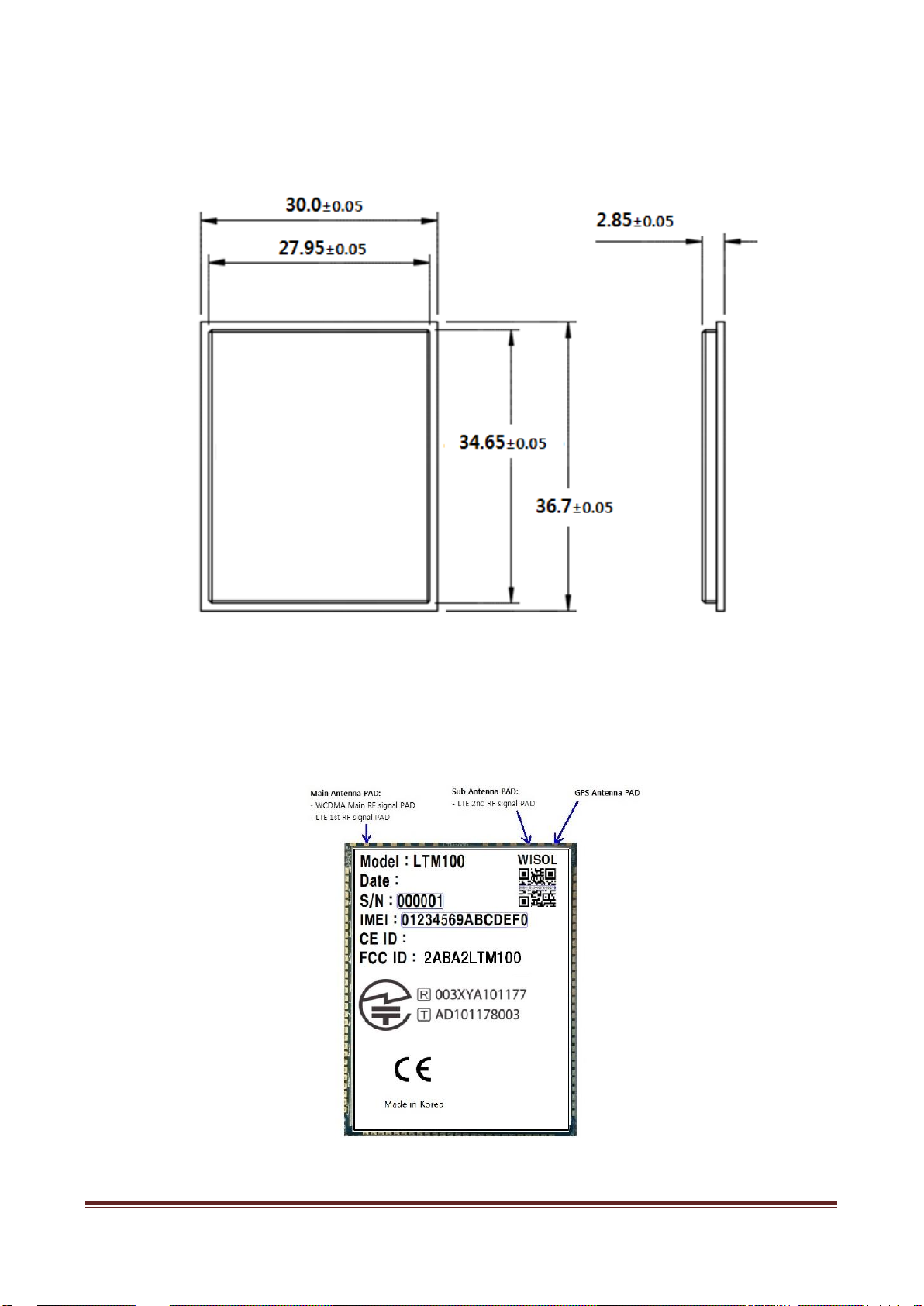
2. 4 Drawing modem
[Top View] (unit: mm)
Figure 2. 1 LTM100 Outline drawing
2. 5 Real Picture
Figure 2. 2 LTM100 Real Picture
WISOL Confidential © 2016 WISOL CO.,LTD. All Rights Reserved 12
Page 13

2. 6 Interface PAD (SMD Type)
This module offers the Interface of 101 PAD Bottom side so that you can send and receive control
data and control by connecting with external devices.
Please design with reference to the description of each of the PAD.
2. 6. 1 101 PAD Detail Outline
Module Bottom PAD(101 ea) are formed as SMD Type as the following drawings
SMT(Surface Mounting Technology) with the customer's device, it can Module, control and
communications
[Bottom View]
Figure 2. 3 LTM100 Bottom Drawing
WISOL Confidential © 2016 WISOL CO.,LTD. All Rights Reserved 13
Page 14

2. 6. 2 101 PAD Description
Voltage Type
1
GND GND - Ground
2
GND GND - Ground
3
EMERGENCY
DOWNLOAD
-
-
For EMERGENCY DOWNLOAD/
internal pull up (Low enable)
4 GPO_01 1.8V Out GPIO output port 01
5 DSR 1.8V Out UART1 Data Set Ready
6 RI 1.8V Out
UART1 Ring Indicator
7 SPI_MOSI 1.8V
Out SPI Master-out Slave-in
8 SPI_MISO 1.8V
In SPI Master-in Slave-out
9 SPI_CLK 1.8V Out Clock for SPI data communication
10 SPI_CS 1.8V Out Chip Selectfor SPI data communication
11 RESOUT_N 1.8V Out RESOUT signal output (Low active)
12 UIM2 Power 1.8/2.95V
Out UIM2 Power
13 UIM2_CLK 1.8/2.95V
- UIM2 Clock
14 UIM2_DATA 1.8/2.95V
- UIM2 Data
15 UIM2_RESET 1.8/2.95V
- UIM2 Reset
16 UIM2_DET 1.8V
In UIM2 Detect signal
17 Reserved
- - Reserved
18 Reserved
- - Reserved
19 Reserved
- - Reserved
20 Reserved
- - Reserved
21
GND GND - Ground
22 USB (-) -
- USB (-) signal
23 USB (+) -
- USB (+) signal
24 HSIC_STB -
- HSIC Strobe
25 HSIC_DATA -
- HSIC Data
26 SDC1_CLK 1.8V
- SDC1 Clock
27 SDC1_CMD 1.8V
- SDC1 Commend
28 SDC1_DATA_3 1.8V
- SDC1 DATA bit 3
29 SDC1_DATA_0 1.8V
- SDC1 DATA bit 0
30 SDC1_DATA_1 1.8V
- SDC1 DATA bit 1
31 SDC1_DATA_2 1.8V
- SDC1 DATA bit 2
32 Codec_I2C_SDA 1.8V
Bath I2C Data (for Codec)
33 Codec_I2C_SCL 1.8V
Out I2C Clock (for Codec)
34 Reserved -
- Reserved
35 Codec_I2S_DATA0 1.8V
- I2S DATA bit 0 (for Codec)
36 Codec_I2S_DATA1 1.8V
- I2S DATA bit 1 (for Codec)
37 Codec_I2S_SCK 1.8V
- I2S Data Clock (for Codec)
38 Codec_I2S_WS 1.8V
- I2S Word Select (for Codec)
39 Reserved 1.8V
- Reserved
40 I2S_MCLK -
Out I2S Master Clock (for Codec)
PAD
No.
PAD name
Input / Output
Remark
Descriptions of Bottom side 101PAD refer to Table 2.5 below.
Table 2. 5 101 PAD description
WISOL Confidential © 2016 WISOL CO.,LTD. All Rights Reserved 14
Page 15

Voltage Type
41 CODEC_RESET_N 1.8V
Out RESET signal output (for Codec)
42 Reserved
- - Reserved
43 Reserved
- - Reserved
44 TXD 1.8V
In UART1 Data Input
45 CTS 1.8V
Out UART1 Clear To Send
46 RXD 1.8V
Out UART1 Data Output
47 RTS 1.8V
In UART1 Ready To Send
48 Reserved -
- Reserved
49 GPI_01 1.8V
In GPIO input port 01
50 GPI_02 1.8V
In GPIO input port 02
51 GPI_03 1.8V In GPIO input port 03
52 UIM1 Power 1.8/2.95V
Out UIM1 Power
53 ADC 1.8V In Analog-to-digital converter
54 Not used
- - Not used
55 USB_VBUS
5.0V In
USB Power
56
GND GND - Ground
57
VBATT 3.8V In Power
58
VBATT 3.8V In Power
59
VBATT 3.8V In Power
60 GPI_04 1.8V In GPIO input port 04
61 GPO_02 1.8V Out GPIO output port 02
62 RESET_N 1.8V In Hardware Reset (low active)
63 Power_on_key 1.8V In Power on/off (Low enable)
64 In_Service_IND 1.8V Out In Service(3G/LTE) Indicate
65
Development key
Dump mode
1.8V In
Dump mode for Software/
internal pull down (High enable)
66 GPO_03 1.8V Out GPIO output port 03
67 GPO_04 1.8V Out GPIO output port 04
68 DTR 1.8V In UART1 Data Terminal Ready
69 DCD 1.8V Out UART1 Data Carrier Detect
70 Not used - - Not used
71 Not used - - Not used
72 Not used - - Not used
73 Not used - - Not used
74 Not used - - Not used
75 Not used - - Not used
76 UIM1_CLK 1.8/2.95V
- UIM1 Clock
77 UIM1_RESET 1.8/2.95V
- UIM1 Reset
78 UIM1_DATA 1.8/2.95V
- UIM1 Data
79 UIM1_DET 1.8V
In UIM1 Detect signal
80 LTE_Service 1.8V Out LTE Service Indicate
81 UART2_TXD 1.8V In UART2 Data Input
82 I2C_SCL 1.8V Out I2C Clock
83 UART2_RXD 1.8V Out UART2 Data Output
84 I2C_SDA 1.8V Both I2C Data
85 GPO_05 1.8V Out GPIO output port 05
PAD
No.
PAD name
Input / Output
Remark
WISOL Confidential © 2016 WISOL CO.,LTD. All Rights Reserved 15
Page 16

note1) In/Out indication of the "Type is based on the module.
PAD
No.
PAD name
Input / Output
Remark
Voltage
Type
57
VBATT
3.8V
In
Power input
58
VBATT
3.8V
In
Power input
59
VBATT
3.8V
In
Power input
1,2
GND
GND
-
Ground
21,56
GND
GND
-
Ground
87,88
GND
GND
-
Ground
90,92
GND
GND
-
Ground
93,94
GND
GND
-
Ground
95,96
GND
GND
-
Ground
97,98
GND
GND
-
Ground
99,101
GND
GND
-
Ground
Voltage Type
86 3G_Service 1.8V Out 3G Service Indicate
87
GND GND - Ground
88
GND GND - Ground
89 GPS_ANT
- - GPS Antenna connection PAD
90
GND GND - Ground
91 SUB_ANT
- - 2nd Antenna connection PAD
92
GND GND - Ground
93
GND GND - Ground
94
GND GND - Ground
95
GND GND - Ground
96
GND GND - Ground
97
GND GND - Ground
98
GND GND - Ground
99
GND GND - Ground
100 MAIN_ANT
- - 1st Antenna connection PAD
101
GND GND - Ground
PAD
No.
PAD name
Input / Output
Remark
note2) Reserved, Not Used pin should not be there, please open a connection with your device.
Module is can be damage and can cause malfunctions muse be urged compliance.
2. 6. 3 Module DC Power Input PADs
The Power supply of the modules are designed to supply hope in the Table below of the Power and
Ground PAD 101 PADs.
Table 2. 6 DC Power Input PADs
note) Please supply VBATT pins have a DC power on 3.4V ~ 4.2V (Typ. 3.8V) range.
WISOL Confidential © 2016 WISOL CO.,LTD. All Rights Reserved 16
Page 17

2. 6. 4 Module Power on/off and Reset control PADs
PAD
No.
PAD name
Input / Output
Remark
Voltage
Type
62
RESET_N
1.8V
In
Modem Hardware Power Reset control (Active Low)
63
Power_on_key
1.8V
In
Modem Power on/off control (Active Low)
Power on / off control of the Module is in a 101 PAD "Power_on_key signal" of PAD number 63,
"Hardware Power Reset" of Module is controlled by the RESET_N signal of the PAD number 62.
Table 2. 7 Power on/off 및 Reset control PADs
When power on as "Figure 2-4" below 1.5s (1,500ms) to over, power off when there 2.0s (2,000ms) is
applied to at least give it high signal on / off operation.
Figure 2. 4 Power On/Off control
Module power on If the condition remains, the pin 36 is High (approximately 1.6V) by the internal
pull-up, to give Module Reset maintain a "Low" signal as shown below 500ms or more if required
by the Low Module It will be Reset.
Figure 2. 5 RESET control
WISOL Confidential © 2016 WISOL CO.,LTD. All Rights Reserved 17
Page 18

2. 6. 5 UART Interface PADs
PAD
No.
PAD name
Input / Output
Remark
Voltage
Type
5
DSR
1.8V
Out
UART1 Data Set Ready
6
RI
1.8V
Out
UART1 Ring Indicator
44
TXD
1.8V
In
UART1 Data Input
45
CTS
1.8V
Out
UART1 Clear To Send
46
RXD
1.8V
Out
UART1 Data Output
47
RTS
1.8V
In
UART1 Ready To Send
68
DTR
1.8V
In
UART1 Data Terminal Ready
69
DCD
1.8V
Out
UART1 Data Carrier Detect
81
UART2_TXD
1.8V
In
UART2 Data Input
83
UART2_RXD
1.8V
Out
UART2 Data Output
PAD
No.
PAD name
Input / Output
Remark
Voltage
Type
55
USB_VBUS
5.0V
In
USB Powet input
22
USB (-)
-
Both
USB (-) signal
23
USB (+)
-
Both
USB (+) signal
24
HSIC_STB - HSIC Strobe
25
HSIC_DATA - HSIC Data
As Interface for "Data terminal equipment"(DTE) and UART data communications, and supports
UART1 and UART2, you can send and receive data by RS-232 data communication requirements.
Table 2. 8 UART Interface PADs
2. 6. 6 USB Interface PADs
As Interface for "Data terminal equipment"(DTE) and USB data communication, in addition to
data communication it can also be used as a Source Download Software and debugging purposes.
Table 2. 9 USB Interface PADs
WISOL Confidential © 2016 WISOL CO.,LTD. All Rights Reserved 18
Page 19

2. 6. 7 External USIM Interface PADs
PAD
No.
PAD name
Input / Output
Remark
Voltage
Type
12
UIM2 Power
1.8/2.95V
Out
UIM2 Power Supply
13
UIM2_CLK
1.8/2.95V
-
UIM2 Clock
14
UIM2_DATA
1.8/2.95V
-
UIM2 Data
15
UIM2_RESET
1.8/2.95V
-
UIM2 Reset
16
UIM2_DET
1.8V
In
UIM2 Detect signal
52
UIM1 Power
1.8/2.95V
Out
UIM1 Power Supply
76
UIM1_CLK
1.8/2.95V
-
UIM1 Clock
77
UIM1_RESET
1.8/2.95V
-
UIM1 Reset
78
UIM1_DATA
1.8/2.95V
-
UIM1 Data
79
UIM1_DET
1.8V
In
UIM1 Detect signal
PAD
No.
PAD name
Input / Output
Remark
Voltage
Type
32
Codec_I2C_SDA
1.8V
Both
Note1) I2C Data (for Codec)
33
Codec_I2C_SCL
1.8V
Out
Note1) I2C Clock (for Codec)
35
Codec_I2S_DATA0
1.8V
-
I2S DATA bit 0 (for Codec)
36
Codec_I2S_DATA1
1.8V
-
I2S DATA bit 1 (for Codec)
37
Codec_I2S_SCK
1.8V
-
I2S Data Clock (for Codec)
38
Codec_I2S_WS
1.8V
-
I2S Word Select (for Codec)
40
I2S_MCLK
-
Out
I2S Master Clock (for Codec)
41
CODEC_RESET_N
1.8V
Out
RESET signal output (for Codec)
53
ADC
1.8V
In
Analog-to-digital converter
82
I2C_SCL
1.8V
Out
Note2) I2C Clock (for external device)
84
I2C_SDA
1.8V
Both
Note2) I2C Data (for external device)
This model is used to select an internal e-SIM, or support the Interface to enable External USIM outside.
Table 2. 10 External USIM Interface PADs
2. 6. 8 Audio and I2C Interface PADs
This Module with I2C Interface is able to control communication with the outside Device, Interface,
which offers support for external Codec.
Table 2. 11 I2C and Audio Interface PADs
note1) These signals are set high by internal pull-up resistor.
note2) These signals require external pull-up resistor.
WISOL Confidential © 2016 WISOL CO.,LTD. All Rights Reserved 19
Page 20

2. 6. 9 SPI and SDIO Interface PADs
PAD
No.
PAD name
Input / Output
Remark
Voltage
Type
7
SPI_MOSI
1.8V
Out
SPI Master-out Slave-in
8
SPI_MISO
1.8V
In
SPI Master-in Slave-out
9
SPI_CLK
1.8V
Out
Clock for SPI data communication
10
SPI_CS
1.8V
Out
Chip Selectfor SPI data communication
26
SDC1_CLK
1.8V
-
SDIO Clock
27
SDC1_CMD
1.8V
-
SDIO Commend
28
SDC1_DATA_3
1.8V
-
SDIO DATA bit 3
29
SDC1_DATA_0
1.8V
-
SDIO DATA bit 0
30
SDC1_DATA_1
1.8V
-
SDIO DATA bit 1
31
SDC1_DATA_2
1.8V
-
SDIO DATA bit 2
PAD
No.
PAD name
Input / Output
Remark
Voltage
Type
3
EMERGENCY DOWNLOAD
- - For EMERGENCY DOWNLOAD (Low enable)
4
GPO_01
1.8V
Out
GPIO output port 01
11
RESOUT_N
1.8V
Out
RESOUT signal output (Low active)
49
GPI_01
1.8V
In
GPIO input port 01
50
GPI_02
1.8V
In
GPIO input port 02
51
GPI_03
1.8V
In
GPIO input port 03
60
GPI_04
1.8V
In
GPIO input port 04
61
GPO_02
1.8V
Out
GPIO output port 02
64
In_Service_IND
1.8V
Out
In Service(3G/LTE) Indicate
65
Development key
1.8V
In
Dump mode for Software (High enable)
66
GPO_03
1.8V
Out
GPIO output port 03
67
GPO_04
1.8V
Out
GPIO output port 04
80
LTE_Service
1.8V
Out
LTE Service Indicate
85
GPO_05
1.8V
Out
GPIO output port 05
86
3G_Service
1.8V
Out
3G Service Indicate
This module also supports SPI and SDIO Interface for additional data communication with external
devices.
Table 2. 12 SPI and SDIO Interface PADs
2. 6. 10 GPIO Interface PADs
Indicating the status of this Module is a GPO and the GPI are available to suit customers' applications ,
As shown below are assigned as the general Input / Output PADs.
Table 2. 13 GPIO Interface PADs
WISOL Confidential © 2016 WISOL CO.,LTD. All Rights Reserved 20
Page 21

2. 6. 11 RF signal PADs
PAD
No.
PAD name
Input / Output
Remark
Voltage
Type
89
GPS_ANT
-
RF
GPS RF connection PAD
91
SUB_ANT
-
RF
2nd RF connection PAD
(LTE 2nd RF signal PAD)
100
MAIN_ANT
-
RF
1st RF connection PAD
(WCDMA Main RF signal PAD
LTE 1st RF signal PAD)
PAD
No.
PAD
name
Input / Output
Remark
Voltage
Type
17,18,19,20,34,39,42,43,48
Reserved
-
-
54,70,71,72,73,74,75
Not Used
-
-
So please RF signal is assigned to the following PADs see Table 2.14 below when connected to the
Antenna.
Table 2. 14 RF signal PADs
2. 6. 12 Reserved and Not Used PADs
Assigned to the pin to the inside of the other uses of this Module,don't need to connect
customer's device, please to open
Table 2. 15 Reserved & Not Used PADs
WISOL Confidential © 2016 WISOL CO.,LTD. All Rights Reserved 21
Page 22

3. Customer PCB Design Guide
3. 1 Customer PCB PAD Design Guide
With reference to the following Figure 3. 1 Design Guide, please design the customer's PCB.
[Top View]
Figure 3. 1 Cusomer PCB Layout Guide
WISOL Confidential © 2016 WISOL CO.,LTD. All Rights Reserved 22
Page 23

3. 2 Installation Guidelines for Antenna PAD
The proper connection between the antenna pad and the application PCB
must be implementing the following installation guidelines for the layout of the application PCB.
a) The whole layer stack below the antenna connection pad should be free of digital lines.
b) Increase GND keep-out (i.e. clearance) around the antenna pad, on the top layer of the
application PCB, to at least 150 µm up to adjacent pads metal definition on the area below the
module, to reduce parasitic capacitance to ground.
c) Add GND clearance on the buried metal layer below the antenna pad,
to reduce parasitic capacitance to ground.
Figure 3. 2 GND clearance on top layer around antenna pad
Figure 3. 3 On the 2nd buried layer below antenna pad
When you intend to install this module(LTM100) with RF connector type,
please refer to the trace guideline figure below. (trace loss: max. 0.3dB)
Figure 3. 4 Trace guideline from the antenna pad to the RF connector pad
WISOL Confidential © 2016 WISOL CO.,LTD. All Rights Reserved 23
Page 24

3. 3 Antenna line Guidelines
Band
Max. Permitted Antenna Gain
WCDMA B2
3.196dBi
WCDMA B4
3.964dBi
WCDMA B5
2.151dBi
LTE B2
3.196dBi
LTE B4
3.964dBi
LTE B5
2.151dBi
GSM850
2.151dBi
GSM1900
3.196dBi
a) Make sure that the impedance of the microstrip line is 50ohm.
b) Reduce the return loss(or V.S.W.R.) as possible with the help of antenna designers.
c) Avoid having other signal tracks and crossing any un-shielded transmission line footprint
with other signal tracks on different layers.
d) The ground surrounding the antenna line should be directly connected to the main ground
plane on the PCB by means of via holes.
e) Place EM noisy devices far away from the antenna line as possible.
f) Keep the antenna line far away from the power supply lines.
4. FCC Warnings and Notices
4. 1 FCC Warnings
The FCC requires the user to be notified that any changes or modifications made to this
module that are not expressly approved by WISOL CO., LTD could void the user's authority
to operate the equipment.
4. 2 Notices
a) If not installed and used in accordance with the instructions on the manual,
this module may cause a malfunction.
In designing this module, please follow the instructions in this manual.
b) Final Installers should be require to satisfy RF exposure compliance for installations and final
host devices.
Compliance of this device in all final host configurations is the responsibility of the guarantee.
The maximum permitted antenna gain including cable loss of the final host device is as follows.
Table 4. 1 The Maximum Permitted Antenna Gain
WISOL Confidential © 2016 WISOL CO.,LTD. All Rights Reserved 24
Page 25

The user manual which is provided by OEM integrators for end users must include the
following information in a prominent location.
“To comply with FCC RF exposure compliance requirements, the antenna used for this
transmitter must be installed to provide a separation distance of at least 20 cm from all
persons and must not be co-located or operating in conjunction with any other antenna
or transmitter.
c) If the FCC ID is not visible when this module(LTM100) is installed inside final host device,
then a label must be affixed to the outside of the final host device with a statement similar
to the following:
"Contains FCC ID: 2ABA2LTM100" or “This device contains FCC ID: 2ABA2LTM100”
WISOL Confidential © 2016 WISOL CO.,LTD. All Rights Reserved 25
Page 26

■ Appendix A
(80pin BtoB connector Type:
LTM100D)
WISOL Confidential © 2016 WISOL CO.,LTD. All Rights Reserved 26
Page 27

■ Appendix A (80pin BtoB connector Type)
A. 1 Air Interface
■ Support Band
- LTE : B1, B4, B5, B7, B11, B18, B19 (Note: LTE B7 does not work in US)
- WCDMA : B1, B2, B4, B5(B6,B19)
- GSM : 850, 900, 1800, 1900
- GNSS(Gen 8C) : GPS, GLONASS, BeiDou, Galileo and QZSS
■ Data Speed
- FDD LTE CAT4 (Down link: 150Mbps / Up link: 50Mbps)
- WCDMA HSPA+ (Down link: 42Mbps / Up link: 5.76Mbps)
※ Data throughput Depending on External communication environment.
■ Air Interface Type (Coaxial Connector 3port)
- U.FL-R-SMT (HIROSE社)
- 3port : 1st / 2nd Antenna 2port, GPS Antenna 1port
A. 2 External Interface
■ DC Power supply : 3.4V ~ 4.2V
■ Communication Interface
- UART : up to 4Mbps Support (2port)
- USB : USB 2.0 Support (1port)
■ USIM Interface
- External UIM card Support (Voltage 1.8V/2.95V)
■ Audio Interface
- Audio : Analog output (2pin)
■ Control Interface
- Control pin : power on, reset, I2C,Status Indicator Output
■ Interface Type (80pin B2B Connector)
- AXK6F80347YG (Panasonic社)
WISOL Confidential © 2016 WISOL CO.,LTD. All Rights Reserved 27
Page 28

A. 3 Module Drawing
Please refer to the following module design drawings.
(Unit: mm)
Figure A-1 Outline Drawing
A. 4 Real Picture
[Top] [Bottom]
Figure A-2 Real Picture
WISOL Confidential © 2016 WISOL CO.,LTD. All Rights Reserved 28
Page 29

A. 5 80pin BtoB connector Specification
Item
Connector P/N
Manufacture
Header/Socket
80pin connector
AXK6F80347YG
Panasonic
Header
Mounted on this Module 80pin BtoB connector Spec(Header)
Pin Numbers
80
Manufacturer
Panasonic
Part number(Mounted on this Module)
AXK6F80347YG (Header)
Connecting Components with external devices is recommended for parts described below.
(80pin Board to Board connector, hereinafter, 80pin BtoB connector)
Table A-1 80pin BtoB connector Specification
※ Customer connector Spec: AXK5F80547YG (Socket Type / Mated height 2.0mm / Panasonic社)
WISOL Confidential © 2016 WISOL CO.,LTD. All Rights Reserved 29
Page 30

Customer connector Spec
Pin numbers
80
Manufacturer
Panasonic
Customer connector Spec
AXK5F80547YG (Socket)
WISOL Confidential © 2016 WISOL CO.,LTD. All Rights Reserved 30
Page 31

A. 6 80pin BtoB connector pin Map
Voltage Type
1 GND GND - Ground
2 Reserved - - note2) reserved
3 Reserved - - note2) reserved
4 GND GND - Ground
5 AD Analog In ADC Input
6 DA Analog Out DAC(PDM) Output
7 Reserved - - note2) reserved
8 VUIM2 1.8/2.95V Out External UIM Power
9 Reserved - - note2) reserved
10 UIM2_RESET/ 1.8/2.95V Out External UIM Reset
11 Reserved - - note2) reserved
12 UIM2_DATA 1.8/2.95V Both External UIM Data
13 Reserved - - note2) reserved
14 UIM2_CLK 1.8/2.95V Out External UIM Clock
15 Reserved - - note2) reserved
16 Reserved - - note2) reserved
17 Not USED - - note2) Not used
18 GPO1 3.0V Out General Output signal 01
19 UART_INIT 3.0V In Reset of the UART data rate
20 AREA_IND 3.0V Out Communication service area indicator
21 PS_HOLD 3.0V Out Modem Power On status indicator
22 RESET_CHK 3.0V Out Module status indicator
23 RI 3.0V Out SMS Receive notification signal
24 DSR 3.0V Out UART1 Data Set Ready
25 DCD 3.0V Out UART1 Data Carrier Detect
26 RTS 3.0V In UART1 Ready To Send
27 CTS 3.0V Out UART1 Clear To Send
28 DTR 3.0V In UART1 Data Terminal Ready
29 RXD 3.0V Out note1) UART1 receiving signal data/DCE(modem) → DTE(customer)
30 TXD 3.0V In note1) UART1 transmitting signal data/DCE(modem) ← DTE(customer)
31 VBATT 3.8V In Power input
32 GND GND - Ground
33 VBATT 3.8V In Power input
34 Reserved - - note2) reserved
35 PWR_ON 2.8V In Power on/off input signal
36 RESET_N 1.8V In External Reset input signal
37 Reserved - - note2) reserved
38 VBATT 3.8V In Power input
39 C_STATUS/GPO2 3.0V Out General Output signal 02
40 VBATT 3.8V In Power input
Pin
No.
Pin name
Input / Output
Remark
Refer to below Table A-2 pin description about 80pin BtoB connector.
Table A-2 80pin BtoB connector pin description
WISOL Confidential © 2016 WISOL CO.,LTD. All Rights Reserved 31
Page 32

Voltage Type
41 GPI1 3.0V In General Input signal 01
42 Not USED - - note2) Not used
43 I2C_SCL 3.0V Out I2C clock signal
44 I2C_SDA 3.0V Both I2C data signal
45 GPI2 3.0V In General Input signal 02
46 GPI3 3.0V In General Input signal 03
47 RXD2 3.0V Out note1) UART2 receiving signal data/DCE(modem) → DTE(customer)
48 TXD2 3.0V In note1) UART2 transmitting signal data/DCE(modem) ← DTE(customer)
49 FUPSTS_OUT/EMG_RI 3.0V Out Emergency ring indicator
50 ANTINF_0 3.0V Out Antenna Information about receiver sensitivity (bit"0")
51 MODE1 3.0V In -
52 ANTINF_1 3.0V Out Antenna Information about receiver sensitivity (bit"1")
53 MODE2 3.0V In -
54 MOS_IND 3.0V Out MRMS Reservation status indicator
55 GND GND - Ground
56 Reserved - - note2) reserved
57 GND GND - Ground
58 Reserved - - note2) reserved
59 Reserved - - note2) reserved
60 Audio_In_P Analog Out note1) Module Audio Positive Output signal
61 Reserved - - note2) reserved
62 Audio_In_N Analog Out note1) Module Audio Negative Output signal
63 GND GND - Ground
64 Reserved - - note2) reserved
65 GND GND - Ground
66 Reserved - - note2) reserved
67 Reserved - - note2) reserved
68 Reserved - - note2) reserved
69 Reserved - - note2) reserved
70 Reserved - - note2) reserved
71 GPI4 3.0V In General Input signal 04
72 VBUS 5.0V In USB Power
73 GPI5/APL_MODE 3.0V In General Input signal 05
74 D- USB Both USB (-) signal
75 RF_CONT 3.0V In airplane mode
76 D+ USB Both USB (+) signal
77 GND GND - Ground
78 GND GND - Ground
79 GND GND - Ground
80 GND GND - Ground
Pin name
Input / Output
Remark
Pin
No.
note1)Pin name of the UART1, UART2, Audio are in your products view.
In practice, Please transmit / receive of the signal, see In / Out of the Type.
note2) Reserved, Not Used pin should not be there, please open a connection with your device.
WISOL Confidential © 2016 WISOL CO.,LTD. All Rights Reserved 32
Page 33

A. 6. 1 Module DC Power Input pins
Pin
No.
Pin name
Input / Output
Remark
Voltage
Type
31
VBATT
3.8V
In
Power input
33
VBATT
3.8V
In
Power input
38
VBATT
3.8V
In
Power input
40
VBATT
3.8V
In
Power input
1
GND
GND
-
Ground
4
GND
GND
-
Ground
32
GND
GND
-
Ground
55
GND
GND
-
Ground
57
GND
GND
-
Ground
63
GND
GND
-
Ground
65
GND
GND
-
Ground
77
GND
GND
-
Ground
78
GND
GND
-
Ground
79
GND
GND
-
Ground
80
GND
GND
-
Ground
Pin
No.
Pin name
Input / Output
Remark
Voltage
Type
35
PWR_ON
2.8V
In
Power on/off input signal (Range: 2.2V ~ 3.0V)
36
RESET_N
1.8V
In
External Reset input signal (Active Low)
The power supply in this module, Please use the following Power and Ground pin of the "80pin
Interface connector pin".
Table A-3 DC Power input pins
note)Please supply VBATT pins have a DC power on 3.4V ~ 4.2V (Typ. 3.8V) range.
A. 6. 2 Module Power on/off and Reset control pins
Module is controlled by the Power on / off the 80 pin connector "PWR_ON signal" of the PAD
number 35, Module Hardware Reset power is controlled by the "RESET_N signal" of the PAD
number 36.
Table A-4 Power on/off and Reset control pins
When power on as "Figure A-4" below 1.5s (1,500ms) to over, power off when there 2.0s (2,000ms)
is applied to at least give it high signal on / off operation.
WISOL Confidential © 2016 WISOL CO.,LTD. All Rights Reserved 33
Page 34

Figure A-3 PWR_ON control
Pin
No.
Pin name
Input / Output
Remark
Voltage
Type
19
UART_INIT
3.0V
In
Reset of the UART data rate
24
DSR
3.0V
Out
UART1 Data Set Ready
25
DCD
3.0V
Out
UART1 Data Carrier Detect
26
RTS
3.0V
In
UART1 Ready To Send
27
CTS
3.0V
Out
UART1 Clear To Send
28
DTR
3.0V
In
UART1 Data Terminal Ready
29
RXD
3.0V
Out
UART1 receiving signal data/DCE(modem) → DTE(customer)
30
TXD
3.0V
In
UART1 transmitting signal data/DCE(modem) ← DTE(customer)
47
RXD2
3.0V
Out
UART2 receiving signal data/DCE(modem) → DTE(customer)
48
TXD2
3.0V
In
UART2 transmitting signal data/DCE(modem) ← DTE(customer)
Module power on If the condition remains, the pin 36 is High (approximately 1.6V) by the internal
pull-up, to give Module Reset maintain a "Low" signal as shown below 500ms or more if required
by the Low Module It will be Reset.
Figure A-4 RESET_N control
A. 6. 3 UART Interface pins
As Interface for "Data terminal equipment"(DTE) and UART data communications, and supports
UART1 and UART2, you can send and receive data by RS-232 data communication requirements.
Table A-5 UART Interface pins
WISOL Confidential © 2016 WISOL CO.,LTD. All Rights Reserved 34
Page 35

A. 6. 4 USB Interface pins
Pin
No.
Pin name
Input / Output
Remark
Voltage
Type
72
VBUS
5.0V
In
USB Power
74
D-
USB
Both
USB (-) signal
76
D+
USB
Both
USB (+) signal
Pin
No.
Pin name
Input / Output
Remark
Voltage
Type
8
VUIM2
2.85V
Out
External UIM Power
10
UIM2_RESET/
2.85V
Out
External UIM Reset
12
UIM2_DATA
2.85V
Both
External UIM Data
14
UIM2_CLK
2.85V
Out
External UIM Clock
Pin
No.
Pin name
Input / Output
Remark
Voltage
Type
43
I2C_SCL
3.0V
Out
I2C clock signal
44
I2C_SDA
3.0V
Both
I2C data signal
60
Audio_In_P
Analog
Out
Module Audio Positive Output signal
62
Audio_In_N
Analog
Out
Module Audio Negative Output signal
As Interface for data terminal equipment (DTE) and USB data communication, in addition to data
communication it can also be used as a Source Download Software and debugging purposes.
Table A-6 USB Interface pins
A. 6. 5 External USIM Interface pins
This model is used to select an internal e-SIM, or support the Interface to enable External USIM outside.
Table A-7 External USIM Interface pins
A. 6. 6 I2C and Analog Interface pins
This Module has to do with I2C Interface External Device communication and control, and
support Audio output.
Table A-8 I2C and Analog Interface pins
WISOL Confidential © 2016 WISOL CO.,LTD. All Rights Reserved 35
Page 36

A. 6. 7 GPIO Interface pins
Pin
No.
Pin name
Input / Output
Remark
Voltage
Type
18
GPO1
3.0V
Out
General Output signal 01
20
AREA_IND
3.0V
Out
Communication service area indicator
21
PS_HOLD
3.0V
Out
Modem Power On status indicator
22
RESET_CHK
3.0V
Out
Module status indicator
23
RI
3.0V
Out
SMS Receive notification signal
39
C_STATUS/GPO2
3.0V
Out
General Output signal 02
49
FUPSTS_OUT/EMG_RI
3.0V
Out
Emergency ring indicator
50
ANTINF_0
3.0V
Out
Antenna Information about receiver sensitivity (bit"0")
52
ANTINF_1
3.0V
Out
Antenna Information about receiver sensitivity (bit"1")
54
MOS_IND
3.0V
Out
MRMS Reservation status indicator
41
GPI1
3.0V
In
General Input signal 01
45
GPI2
3.0V
In
General Input signal 02
46
GPI3
3.0V
In
General Input signal 03
51
MODE1
3.0V
In - 53
MODE2
3.0V
In - 71
GPI4
3.0V
In
General Input signal 04
73
GPI5/APL_MODE
3.0V
In
General Input signal 05
75
RF_CONT
3.0V
In
airplane mode
5
AD
Analog
In
ADC Input
6
DA
Analog
Out
DAC(PDM) Output
Pin
No.
Pin name
Input / Output
Remark
Voltage
Type
2,3,7,9,11,13,15,16,
34,37,56,58,59,61,
64,66,67,68,69,70
Reserved
-
17,42
Not USED
-
-
Indicating the status of this Module is a GPO and the GPI are available to suit customers' applications ,
As shown below are assigned as the general Input / Output PADs.
Table A-9 GPIO Interface pins
A. 6. 8 Reserved and Not USED pins
Assigned to the pin to the inside of the other uses of this Module,don't need to connect
customer's device, please to open
WISOL Confidential © 2016 WISOL CO.,LTD. All Rights Reserved 36
Table A-10 Reserved & Not USED pins
Page 37

A. 7 Antenna Connector Specification description
구 분
Connector P/N
Manufacturer
notes
Antenna connection
connector
U.FL-R-SMT
Hirose
3 port
(LTE 2port,
GPS 1port)
Antenna connector Specification
Manufacturer
Hirose
Part number(Mounted on this Module)
U.FL-R-SMT
This module had three of the external antenna port.
LTE Primary or WCDMA(3G) Antenna 1 port , LTE Secondary Antenna 1 port,
GPS Antenna 1 port.
The antenna port may be connected to the customer's device antenna.
A. 7. 1 Antenna Connector Specification
Table A-11 Antenna connector Specification
WISOL Confidential © 2016 WISOL CO.,LTD. All Rights Reserved 37
Page 38

A. 7. 2 Antenna Connector Description
For Antenna connector locations, see the Figure A-6 below.
Figure A-5 Antenna Connector
WISOL Confidential © 2016 WISOL CO.,LTD. All Rights Reserved 38
Page 39

A. 8 Module Assembly Guide
A. 8. 1 Module Assembly Instruction
When this Module mounted on the Board(PCB) assembled by the customer,
please refer to Figure A-7.
Please fix the Module each three screws and nuts.
When the assembly while power is on customer during assembly in customers' Board,
Damage given in this Module, please note that it may be a problem such as a power failure and
malfunction occurred.
fixed screw: M2.0 X d mm
d = 2.8 + t + 3.0 ± 0.2mm (t : Customer device PCB thickness)
Notice) fixed screw tighten torque: 1.2 ± 0.2kgfcm (Don't tighten the screw to more than 1.5kgfcm)
Figure A-6 Module Assembly Instruction
WISOL Confidential © 2016 WISOL CO.,LTD. All Rights Reserved 39
Page 40

A. 9 Customer PCB Board Layout Guide
GND
Board Layout of customers design, please refer to the drawing below
Figure A-7 Customer PCB Layout Guide
WISOL Confidential © 2016 WISOL CO.,LTD. All Rights Reserved 40
 Loading...