

Page 1

Version 1.0
page 1 of 15
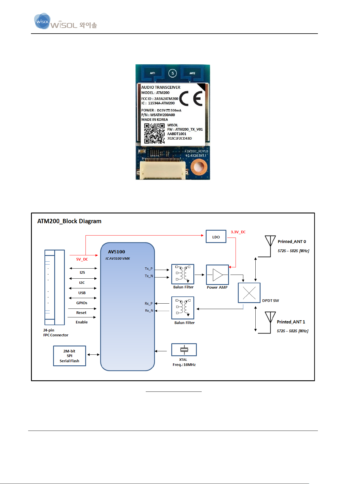
ATM200
User Manual
1. Introduction
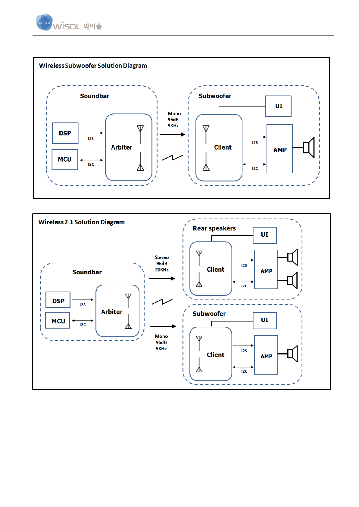
The ATM200 is a 5GHz wireless audio transceiver module offering point to multi-point digital wireless audio solutions
such as wireless subwoofers and wireless rear speakers and in home theater system.
The module incorporates AV5100 SoC (System-on-chip) with Avnera’s proprietary 5GHz wireless audio protocol to
accommodate a wide range of wireless audio application. It features low fixed latency, multiple OTA audio
configurations, uncompressed CD quality mono or stereo audio, excellent interference immunity, and inherent
coexistence with WIFI.
The AV5100 SoC contains all the necessary radio transceiver and digital baseband circuitry to form a complete digital
wireless node without external processing as well as including power management and analog circuitry to operate it.
The module integrates all feature necessary to complete a wireless link including wireless audio IC, power amplifier (PA),
flash memory, printed diversity antennas, FPC connector and passive components. It provides better extended wireless
range with external PA and user interfaces through 24pin FPC connector.
The ATM200 module is certified to FCC and CE standards.
2. Feature
Product Size
- Module Size (mm): 40.4 (W) X 26.0 (L) X 3.1 (H)
- PCB size (mm): 40.0 (W) X 2.6.0 (L) x 1.1 (H)
- Shield can (mm): 24.7 (W) X 21.9 (L) X 2.0(H)
- Antenna Type : PCB Printed Antenna
Audio Interfaces
- I2S Digital Input/Output interface with >93dB end-to-end digital audio path
5.725-5.825 GHz RF operating frequency band
Low, fixed latency (14.8ms typ. for stereo)
3Mbps OTA data rate
Multiple OTA audio configurations
Forward error correction coding, error detection, and audio-specific error concealment
Auto-search/sync and dynamic channel selection
Capability to detect and avoid wideband interferences such as 5GHz band WLAN
Dual printed PCB diversity antennas for multipath and fading migrations
Wireless Range (typ.)
- NLOS (Non Line Of Sight) range : >50m
- LOS (Line of Sight) range : > 160m
I2S digital audio capability
Page 2
Version 1.0
page 2 of 15
24pin FPC connector
Applications : Wireless Subwoofers, Wireless Rear speakers, Soundbar, AV Receiver
3. Block Diagram
ATM200
.ATM200 block diagram
The ATM200 module is available in two variations; digital input transmitter or digital output receiver.
There are three available I2S digital audio data inputs/outputs, each of these can be configured to operate as either a master
Page 3
Version 1.0
page 3 of 15
I/O interfaces
Description
+5.0V supply
The ATM200 module is configured to accept a nominal +5.0V supply.
Reset
Active low reset input. This pin is driven from an open collector/drain device such that it can be
pulled to ground for the active reset state but, when released, must go to a high impedance state.
This pin should not be actively driven high, as the AV5100 internal reset circuit will not operate
correctly.
I2S In Port
The I2S input port can be configured as a master or slave. Consequently BCLK and LRCK can
be either inputs or outputs. In addition, MCLK can be sourced by the module. Since the AV5100
IC contains a sample rate converter, MCLK is not required to be supplied to the module when it
is an I2S slave. CMOS 3.3V logic levels are used for all I2S signals.
I2S Out Port
The I2S output port can be configured as a master or slave. Consequently BCLK and LRCK can
be either inputs or outputs. In addition, MCLK can be sourced by the module. Since the AV5100
IC contains a sample rate converter, MCLK is not required to be supplied to the module when it
is an I2S slave. CMOS 3.3V logic levels are used for all I2S signals.
I2C Slave Port
The I2C slave port can be used for external host communication and for module testing. It is
assumed that external pull up resistors are connected at the I2C master communicating with the
module.
I2C Master Port
The I2C master port is used to communicate with external audio devices such as a sub-woofer
amplifier or rear speaker. It is assumed that external pull up resistors are included on the
application board.
GPIOs
3.3V CMOS logic level GPIOs available to connect to other devices, or to use as UI supporting
GPIOs for LED and button support. All supported GPIOs can be configured as outputs or inputs
with configurable pull-ups/pull-downs.
ATM200
or a slave – depending on the application, the I2S ports can operate simultaneously as either inputs or outputs. When
configured as slaves, the I2S inputs/outputs can be independently clocked by up to two external masters. In addition,
MCLK can be output from the module to provide a reference clock source to an external ADC or DAC. MCLK can also be
input to the module to provide a reference clock from an external source.
The hardware for the audio input (transmit) and audio output (receive) versions of the module is identical and only the
firmware loaded onto the module determines its function.
The highly integrated nature of the AV5100 transceiver IC results in few external components being required for the
ATM200 module design. 2 printed PCB antennas are used to achieve increased range, and to achieve antenna spatial
diversity. The extended-range RF path consists of the antennas, associated tuning components, shield can, the RF switch,
RF power amplifier (PA) and two baluns, one connected to each of the RF input/output ports on the AV5100 IC.
A 16MHz crystal oscillator generates the AV5100 fundamental system clock used as the basis for all RF and digital audio
clocks.
A 2Mb flash memory chip is used to store the module’s application firmware. The AV5100 is able to boot from internal
ROM upon first power up, which enables programming the flash chip with the application firmware through USB. In
addition, Over-the-air Firmware upgrade capability can be enabled through the application firmware. The module can be
controlled from an external host device via the I2C Slave or the SPI Slave data interfaces. The I2C master port allows the
module to control other system audio devices such as a sub-woofer amplifier system without having to add another MCU
to the product design. Up to 9 additional GPIOs are available on the ATM200 module (not including I2C and I2S signals)
for implementing different UI features on the target application.
I/O interfaces description
Page 4
Version 1.0
page 4 of 15
4. Functional Diagram
ATM200
Page 5
Version 1.0
page 5 of 15
CONDITION
MIN
MAX
+5V Supply Voltage Input
-0.3V
6.0V
Input Voltage Range – Digital Inputs
-0.3V
3.6V
Input Voltage Range – Analog Inputs
-0.3V
3.6V
Operating Temperature
-40ºC
+60ºC
Storage Temperature
-40ºC
Static Discharge Voltage*
Level 2
PARAMETER
MIN
TYP
MAX
UNIT
VDD, +5V Supply pin voltage
4.5
5.0
5.5
V
Ambient Temperature (TA)
0 55
ºC
RESET pin hold time
10
ms
Power Supply Rise Time (to 3.0V)
0 10
ms
PARAMETER
CONDITION
MIN
TYP
MAX
UNIT
Supply Current (IVDDA)
Shutdown (chip disabled)
TBD 1 uA
ATM200
5. Electrical Specifications
Absolute Maximum Ratings
Absolute Maximum Ratings (AMR) are stress ratings only. AMR corresponds to the maximum value that can be applied without leading
to instantaneous or very short-term unrecoverable hard failure (destructive breakdown). Stresses beyond those listed under AMR may
cause permanent damage to the device.
Functional operation of the device at these or any other conditions beyond those indicated under “Recommended Operating Range” is
not implied. Exposure to absolute-maximum-rated conditions for extended periods may adversely affect device reliability.
Device functional operating limits and guaranteed performance specifications are given under Electrical Characteristics at the test
conditions specified.
Notes;
* System level ESD : IEC 61000-4-2; C = 150pF, R = 330Ω
Recommended operating Range
Electrical Characteristics – DC
Operating Conditions: VDD = 4.5 to 5.5V, TA = 0°C to +55 °C, RF Freq = 5725‐5825MHz, measured relative to the RF balun single‐ended I/O.
Typical specifications at TA = 25°C, VDD = 5.0V
Page 6

Version 1.0
page 6 of 15
Standby (also USB suspend)
TBD
2.5
mA
RX mode (continuous RX)
89
mA
Link mode for TX
270
Link mode for RX
130
TX mode (continuous TX);
Pout=+13dBm
350
CMOS I/O Logic Levels –
VDDIO 3.3V
Input Voltage Logic Low, VIL
0.6
V
Input Voltage Logic High, VIH
VDDIO -
0.6V
Output Voltage Logic Low,
VOL
0.3
Output Voltage Logic High,
VOH
VDDIO -
0.3V
PARAMETER
CONDITION
MIN
TYP
MAX
UNIT
RF Channel Frequency Range
Upper band (Band 4)
5725
5825
MHz
TX Output power
FCC compliance
10
13
18
dBm
CE compliance
6 9 14
TX Spurious(harmonic)
2nd
-55
dBm
3rd
-65
dBm
RF I/O Impedance
ANT0, ANT1
50 ohm
LO leakage
-20 dBc
PARAMETER
CONDITION
MIN
TYP
MAX
UNIT
RF Channel Frequency Range
Upper band (Band 4)
5725
5825
MHz
RX Sensitivity
SSC (single sub-carrier)
-90 *
dBm
Max input signal
LNA = low gain mode,
min IF gain
-5
Out-of-band blocker level
<5150 MHz, >5850 MHz
-45
Electrical Characteristics – RF TX
Operating Conditions: VDD = 4.5 to 5.5V, TA = 0°C to +55 °C, RF Freq = 5725‐ 5825MHz, measured relative to the RF balun single‐ ended
I/O. Typical specifications at TA = 25°C, VDD = 5.0V
ATM200
Electrical Characteristics – RF RX
Operating Conditions: VDD = 4.5 to 5.5V, TA = 0°C to +55 °C, RF Freq = 5725‐ 5825MHz, measured relative to the RF balun single‐ ended
I/O. Typical specifications at TA = 25°C, VDD = 5.0V
Page 7

Version 1.0
page 7 of 15
2400-2483.5 MHz
-20
Spurious RF outputs
5150-5850 MHz
-55
<5150 MHz, >5850 MHz
-63 dBm
RF I/O Impedance
ANT0, ANT1
50 ohm
PARAMETER
CONDITION
MIN
TYP
MAX
UNIT
RF Channel Frequency Range
Upper band (Band 4)
5725
5825
MHz
RF Channel frequency resolution
(raster)
1 MHz
Local Frequency error
5
10
ppm
Crystal Oscillator Frequency
External crystal
16 MHz
RF I/O Impedance
ANT0, ANT1
50 ohm
* The sensitivity been defined with BER <= 0.002.
Electrical Characteristics – RF PLL
Operating Conditions: VDD = 4.5 to 5.5V, TA = 0°C to +55 °C, RF Freq = 5725‐5825MHz, measured relative to the RF balun single‐ended I/O.
Typical specifications at TA = 25°C, VDD = 5.0V
ATM200
Antenna Characteristics
VSWR
Page 8

Version 1.0
page 8 of 15
Antenna Gain
ANT0
ATM200
ANT1
Page 9

Version 1.0
page 9 of 15
Pin Number
Pin Name
I/O
Description
1
GPIO2 /S_SSB
I/O
SPI slave chip select
2
GPIO3 /S_SCLK
I/O
SPI slave serial clock
3
GPIO4 / I2CS_SDA/S_MOSI
I/O
I2C slave serial data or SPI slave data In
4
GPIO5 / I2CS_SCL/S_MISO
I/O
I2C slave serial clock or SPI slave data out
5
GPIO16 / I2CM_SDA
I/O
I2C master serial data
6
GPIO17 / I2CM_SCL
I/O
I2C master serial clock
7
GPIO20 /LINK_LED
I/O
Link_LED output
8
GPIO21/ PAIR
I/O
Input from PAIR Button
9
GPIO18 /BCK1
I/O
I2S port1 bit clock
10
GPIO19 / WCLK1
I/O
I2S port1 word clock
11
GPIO10 /MCLK
I/O
Master clock out
12
GND
GND
GND
13
GPIO11 / BCK0
I/O
I2S port0 bit clock
14
GPIO12 /WCLK0
I/O
I2S port0 word clock
15
GPIO13 /ADAT0
I/O
I2S port0 audio data
16
GPIO14 / ADAT1
I/O
I2S port1 audio data
17
GPIO15 / ADAT2/CEN
I/O
I2S port2 audio data or Chip enable
18
GPIO22 / D+
I/O
USB data plus
19
GPIO23 / D-
I/O
USB data minus
20
GPIO24
I/O
GPIO
21
RESETN_EXT
I
Reset signal active low
22
GND
GND
GND
23
VDD
PWR
+5.0V input supply voltage
24
VDD
PWR
+5.0V input supply voltage
Pin #1
Pin #24
I/O Pin Description
ATM200
Page 10

Version 1.0
page 10 of 15
Parameter
MIN
TYP
MAX
UNIT
Notes
V
L
Low voltage level
-0.3 0 0.4
V
VL
High voltage level
2.4
3.3
3.6
V
T
Clock period
325.5 ns
1/3.072MHz
TLO
Clock low period
0.4T
0.6T
THI
Clock high period
0.4T
0.6T
TR
Rise time
50
ns
TF
Fall time
50
ns TSu
Setup time
25
ns
THd
Hold time
25
ns
TOd
Output delay
-25 25
ns
Bit clocks/Word clock
64
I2S Communication Interface Timing
I2S Interface Timing
ATM200
Page 11

Version 1.0
page 11 of 15
Parameter
MIN
MAX
UNIT
V
IL
Low level input voltage
-0.3
0.8
V
VIH
High level input voltage
2.0
3.6
V
VOH
Low level output voltage
At 1mA sink current
0
0.4
V
tof
Output fall time from V
IHmin
to V
ILmax
with a bus capacitance from 10pF to 400pF
0
250
ns
tSP
Pulse width of spike which must be suppressed by the
input filter
0
50
ns
f
SCL
S_SCL clock frequency
0
400
KHz
t
LOW
Low period of the S_SCL clock
1.3
ns
T
HIGH
High period of the S-SCL clock
0.6
ns
tHD;DAT
Data hold time
100
ns
TSU;DAT
Data set-up time
100
ns
I2C Slave Communication Interface Timing
I2C Slave Interface Timing (Fast-Mode)
ATM200
Page 12

Version 1.0
page 12 of 15
6. Label
ATM200 TX Module Label
1) FCC & CE
ATM200
2) FCC only
Page 13

Version 1.0
page 13 of 15
ATM200 RX Module Label
1) FCC & CE
ATM200
2) FCC only
Page 14

Version 1.0
page 14 of 15
his device complies with Part 15 of FCC Rules, Operation is Subject to following two conditions:
(1) This device may not cause harmful interference, and
(2) This device must accept any interference received including interference that cause undesired operation.
Caution: Any changes or modifications to the equipment not expressly approved by the party responsible for
compliance could void user s authority to operate the equipment.
This equipment has been tested and found to comply within the limits for a Class B digital device, pursuant to
part 15 of the FCC Rules. These limits are designed to provide reasonable protection against harmful
interference in a residential installation.
This equipment generates, uses, and can radiate radio frequency energy and, if not installed and used in
accordance with the instructions, may cause harmful interference to radio communications. However, there
is no guarantee that interference will not occur in a particular installation. If this equipment does cause
harmful interference to radio or television reception, which can be determined by turning the equipment off
and on, the user is encouraged to try to correct the interference by one or more of the following measures:
• Reorient or relocate the receiving antenna
• Increase the separation between the equipment and receiver
• Connect the equipment into an outlet on a different circuit from that to which the receiver is connected
• Consult the dealer or an experienced radio/TV technician for help.
IMPORTANT NOTE:
FCC Radiation Exposure Statement;
This appliance and its antenna must not be co-located or operation in conjunction with any other antenna or
transmitter.
A minimum separation distance of 20 ㎝ must be maintained between the antenna and the person for this
appliance to satisfy the RF exposure requirements.
USER MANUAL OF THE END PRODUCT:
In the users manual of the end of product, the end user has to be informed to keep at least 20cm separation
with the antenna while this end product is installed and operated.
LABEL OF THE END PRODUCT:
The module is labeled with its own FCC ID and IC Certification Number. If the FCC ID and IC
Certification Number are not visible when the module is installed inside another device, then the
outside of the device into which the module is installed must also display a label referring to the
enclosed module. In that case, the final end product must be labeled in a visible area with the
following:
7. Notice
FCC/ISED Statement
ATM200
Page 15

Version 1.0
page 15 of 15
T Le présent appareil est conforme aux CNR d’Industrie Canada applicables aux appareils radio exempts de licence.
L’exploitation est autorisée aux deux conditions suivantes :
(1) l’appareil ne doit pas produire de brouillage, et
(2) l’utilisateur de l’appareil doit accepter tout brouillage radioélectrique subi, même si le brouillage est susceptible
d’en compromettre le fonctionnement.
Cet appareil numérique de la classe B est conforme á la norme NMB-003 du Canada.
l'exposition aux RF
L’antenne (ou les antennes) doit être installée de façon à maintenir à tout instant une distance minimum de au moins 20
cm entre la source de radiation (l’antenne) et toute personne physique.
Étiquetage du produit final (IC)
Le module BT111 est étiqueté avec sa propre identification FCC et son propre numéro de certification IC. Si
l’identification FCC et le numéro de certification IC ne sont pas visibles lorsque le module est installé à l’intérieur d’un
autre dispositif, la partie externe du dispositif dans lequel le module est installé devra également présenter une étiquette
faisant référence au module inclus. Dans ce cas, le produit final devra être étiqueté sur une zone visible avec les
informations suivantes :
« Contient module émetteur identification FCC ID : 2ABA2ATM200
« Contient module émetteur IC: 11534A-ATM200”
Hereby, WISOL CO., LTD declares that the radio equipment type AUDIO TRANSCEIVER is in compliance with
Directive 2014/53/EU. The full text of the EU declaration of conformity is available at the providing datasheet or
approval sheet.
The antenna(s) must be installed such that a minimum separation distance of at least 20 cm is maintained between the
radiator (antenna) and all persons at all times. This device must not be collocated or operating in conjunction with any
other antenna or transmitter.
IC Statement
CE Statement
CE Statement
ATM200
 Loading...