

Page 1

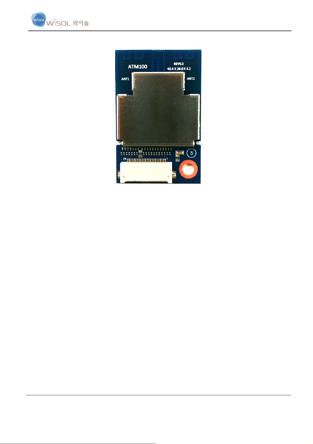
ATM100
OEM Integrators / User Manual
1. Introduction
The ATM100 module offers customers fast time to market with a mono, or stereo, wireless audio connection. The module
is optimized for low-cost, high-quality, easy-to-use wireless audio solutions for wireless subwoofer or wireless rear speaker
applications.
Avnera’s proprietary wireless system takes a new approach to wireless audio. The wireless protocol was designed from the
ground up and delivers uncompressed mono or stereo audio, with fixed latency over the air, without interference issues,
and with industry leading WiFi coexistence – even at close proximities to a WiFi device.
Avnera-enabled wireless modules offer a low-touch, easy-to-integrate wireless audio solution and enables fast time to
market by eliminating concerns about compliance, antenna tuning, and board optimization.
Modules based on Avnera’s AV6210 silicon provide breakthrough wireless audio functionality with fixed low-latency
point-to-point transport of uncompressed mono/stereo PCM audio data supporting a wide range of input sample rates. A
single I2S digital audio port is used for the module audio input/output.
2. Feature
Product Size
‐ Module Size (mm): 40.4 (W) X 26.0 (L) X 3.2 (H)
‐ Antenna Type : PCB Printed Antenna
Audio Interfaces
‐ I2S Digital Input/Output interface with >94dB end-to-end digital audio path
2.4 GHz ISM band, continuous dynamic channel selection
Forward error correction coding, error detection, and audio-specific error concealment
Dual onboard printed PCB antennas for multipath and fading mitigation
Auto-search/synch and dynamic channel selection
Low, fixed latency of less than 20ms for typical audio applications
24 pin FPC or pin header connector
Sample rate converter: Support for 32 - 96kHz input sample rates
Over-the-air upgrade capability
Customizable firmware for simple, low-cost, sub-woofer amplifier implementations
General purpose over-the-air (OTA) serial interface:
> 11 kbps, bi-directional, full duplex
Support for amplifier control data, meta-data data, and remote commands
Version 1.0 page 1 of 14
Page 2
ATM100
3. General Function
The ATM100 module is available in 2 variations; digital input transmitter module or digital output receiver module. There
is a separate I2S port for digital audio input and output functions and either of these can be configured to be a master or a
slave – only the input or output port can be active at any time. In addition, MCLK can be generated from the module, or
input to the module as required by the system application.
The highly integrated nature of the AV6210 transceiver IC results in few external components being required for the
ATM100 module design. 2 PCB antennas are used to achieve increased range, and to offer diversity, and the simple RF
path consists only of the antennas, associated tuning components, the RF switch and a LC balun connected to the AV6210
IC. A 16MHz crystal generates the AV6210 system clock signal used as the basis for all RF and digital audio signals. In
addition, a 2Mb flash memory stores the factory based firmware, as well as firmware upgrade images and configuration
parameters. The module firmware enables upgrades to be performed by the I2C slave interface or over-the-air. The module
can be controlled from an external host device via the I2C interface. The I2C master port allows the module to control
other system audio devices such as a sub-woofer amplifier system without having to add another MCU to the product
design. Up to a maximum of 17 GPIOs are supported with the ATM100 module including I2C and I2S signals. This large
number of GPIOs can be leveraged to Implement low cost sub-woofer designs as outlined below.
The ATM100 module offers a standard and low latency firmware with different over the air sample rate. While the
standard 22.2KSps over the air sample rate optimizes audio quality and WiFi coexistence performance; Lower audio
latency can be achieved by using the low-latency 44.4KSps over the air sample rate.
Version 1.0 page 2 of 14
Page 3
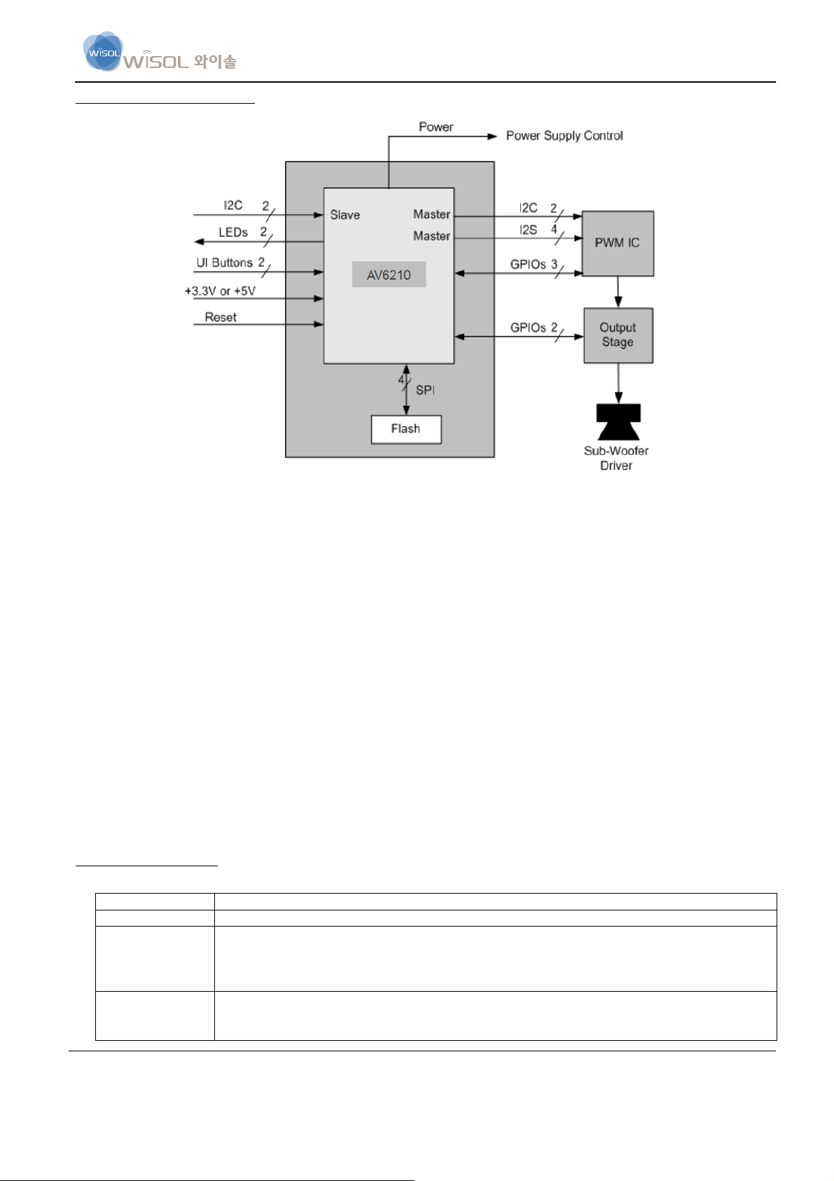
Typical Sub-Woofer Implement
ATM100
A simple low cost implementation of a sub-woofer product design is shown in Figure 2. The sub amplifier consists of a
PWM chip plus an output stage device, but no external MCU is required as the ATM100 RX module performs the control
function using the I2C master communication port in conjunction with multiple GPIOs. +5V power and
an optional reset signal are supplied to the ATM100 RX module and I2C slave communication can be used to control the
module if required. Several GPIOs can be used to drive LEDs, or to connect to UI buttons. Typically 2 LEDs may be used
and 1 button for pairing purposes. Another button could be used, for example, to implement a “bass enhance” feature.
Another GPIO can be used to control the main power supply for the unit. The ATM100 RX module will remain always
powered up but a GPIO control line is used to enable/disable the higher voltage rail for the amplifier output circuitry. If the
wireless link is lost (when the sound bar, or ATM100 TX module is powered down) the ATM100 RX module can, after a
timeout period, power down the amplifier section to conserve power and to help meet energy start requirements.
The I2C master port from the ATM100 RX module can communicate, control, and initialize external audio ICs such as the
PWM chip in this example.
Other GPIOs can be used to detect fault conditions (over temperature etc) and notify the module. The audio is routed from
the ATM100 RX module to the amplifier circuit with the I2S output port which can be configured as either a master or a
slave as required. MCLK can also be generated from the SWA RX module as a ~12.288MHz clock if required.
I/O interfaces description
I/O interfaces Description
+5.0V supply The ATM100 module is configured to accept a nominal +5.0V supply.
Reset Active low reset input. This pin is driven from an open collector/drain device such that it can be
pulled to ground for the active reset state but, when released, must go to a high impedance state.
This pin should not be actively driven high, as the AV5100 internal reset circuit will not operate
correctly.
I2S In Port The I2S input port can be configured as a master or slave. Consequently BCLK and LRCK can
be either inputs or outputs. In addition, MCLK can be sourced by the module. Since the AV5100
IC contains a sample rate converter, MCLK is not required to be supplied to the module when it
Version 1.0 page 3 of 14
Page 4
ATM100
is an I2S slave. CMOS 3.3V logic levels are used for all I2S signals.
I2S Out Port
I2C Slave Port
I2C Master Port
GPIOs 3.3V CMOS logic level GPIOs available to connect to other devices, or to use as UI supporting
The I2S output port can be configured as a master or slave. Consequently BCLK and LRCK can
be either inputs or outputs. In addition, MCLK can be sourced by the module. Since the AV5100
IC contains a sample rate converter, MCLK is not required to be supplied to the module when it
is an I2S slave. CMOS 3.3V logic levels are used for all I2S signals.
The I2C slave port can be used for external host communication and for module testing. It is
assumed that external pull up resistors are connected at the I2C master communicating with the
module.
The I2C master port is used to communicate with external audio devices such as a sub-woofer
amplifier or rear speaker. It is assumed that external pull up resistors are included on the
application board.
GPIOs for LED and button support. All supported GPIOs can be configured as outputs or inputs
with configurable pull-ups/pull-downs.
4. Electrical Specifications
Absolute Maximum Ratings
Absolute Maximum Ratings (AMR) are stress ratings only. AMR corresponds to the maximum value that can be applied
without leading to instantaneous or very short-term unrecoverable hard failure (destructive breakdown). Stresses beyond
those listed under AMR may cause permanent damage to the device.
Functional operation of the device at these or any other conditions beyond those indicated under “Recommended Operating
Range” is not implied. Exposure to absolute-maximum-rated conditions for extended periods may adversely affect device
reliability.
Device functional operating limits and guaranteed performance specifications are given under Electrical Characteristics at
the test conditions specified.
CONDITION MIN MAX
+5V Supply Voltage Input -0.3V 6.0V
Input Voltage Range – Digital Inputs -0.3V 3.6V
Operating Temperature -10ºC +70ºC
Storage Temperature -20ºC +80ºC
Version 1.0 page 4 of 14
Page 5
Recommended operating Range
PARAMETER MIN TYP MAX UNIT
VDD, +5V Supply pin voltage 4.5 5.0 5.5 V
Ambient Temperature (TA) 0 60 ºC
Electrical Characteristics – DC
PARAMETER CONDITION MIN TYP MAX UNIT
TX Module Configuration Linked 35 mA
TX Module Configuration Searching 22 mA
TX Module Configuration Continuous TX 63 mA
ATM100
RX Module Configuration Linked 35 mA
Electrical Characteristics – RF TX/RX
Operating Conditions: VDD = 4.5 to 5.5V, TA = 0°C to +60 °C, RF Freq = 2403.35-2477.35MHz, measured at RF
test connector. Typical specifications at TA = 25°C, VDD = 5.0V
PARAMETER CONDITIONS MIN TYP MAX UNIT
RF Channel Frequency Range 2403.35 2477.35 MHz
TX Output power 2.5 dBm
RX Sensitivity -88.7 dBm
Range (NLOS) 15 m
Range (LOS) 50 m
Notes;
1) Sensitivity is defined as the onset of 0.2% BLER Clock Error Rate.
Version 1.0 page 5 of 14
Page 6

ATM100
Electrical Characteristics – Audio
Operating Conditions: VDD = 4.5 to 5.5V, TA = 0°C to +60 °C, RF Freq = 2403.35-2477.35MHz, measured at RF
test connector. Typical specifications at TA = 25°C, VDD = 5.0V
PARAMETER CONDITION MIN TYP MAX UNIT
Frequency Response1) 20 10K Hz
Gain Flastness2) 0dB Input/Output Gain
±0.2
dB
SNR I2S Input/Output 94 dB
THD+N
Notes;
1) 16 bit audio, 22.2KSps over-the-air sample rate firmware build
2) 16 bit audio, 22.2KSps over-the-air sample rate firmware build – 10KHz frequency response
Electrical Characteristics – Audio latency
Operating Conditions: VDD = 4.5 to 5.5V, TA = 0°C to +60 °C, RF Freq = 2403.35-2477.35MHz, measured at RF
test connector. Typical specifications at TA = 25°C, VDD = 5.0V
94 dB
PARAMETER CONDITION MIN TYP MAX UNIT
22.2KSps OTA Sample latency Standard Firmware 17 ms
44.4KSps OTA Sample latency Standard Firmware 14 ms
Antenna Characteristics
PARAMETER CONDITION MIN TYP MAX UNIT
Frequency Range 2400 2480 MHz
ANT1 1.92:1
VSWR
ANT2 2.23:1
Peak Gain 4.8 dBi
ANT1 70.2 %
Efficiency
ANT2 63.8 %
Isolation -14 dB
Impedance 50 Ω
Version 1.0 page 6 of 14
Page 7

ATM100
I/O Pin Description
No Pin Name I/O Description
1 VDD PWR +5.0V input supply
AVM100
TX Module
voltage
2 VDD PWR +5.0V input supply
voltage
3 GPIO I/O Function defined by
GPIO ADOUT0 RX =
firmware application
4 GPIO I/O Function defined by
GPIO GPIO
firmware application
5 GPIO
6 Reset I Driven from open drain
I/O Function defined by
firmware application
GPIO GPIO
Reset Reset
external source.
Can be left open
7 I2C_SCL_S /
S_MISO
8 I2C_SDA_S /
S_MOSI
I/O I2C slave or SPI slave
port
I/O I2C slave or SPI slave
port
I2C_SCL_S LED RED,
I2C_SDA_S LED RED,
9 I2C_SCL_M O I2C master or GPIO GPIO I2C_SCL_M
10 I2C_SDA_M I/O I2C master or GPIO GPIO I2C_SCL_M
11 S_SCLK I SPI slave port or GPIO GPIO GPIO
12 GND GND Ground
13 BCK1 I/O I2S port BCLK1, TX module
= Input
14 WCLK1 I/O I2S port WCLK1, TX module
= Input
15 S_SSB I SPI slave port or GPIO GPIO GPIO
16 MCLK I/O I2S port or GPIO GPIO/MCLK RX = 12.000MHz
17 ADIN1 I/O I2S port ADIN1, TX module
= Input
18 M_SSB/GPIO17 O SPI master port or GPIO GPIO GPIO
19 M_SCLK/GPIO1 O SPI master port or GPIO GPIO GPIO
20 M_MOSI O SPI master port NC NC
21 M_MISO I SPI master port NC NC
22 GPIO I/O Function defined by
LED1 BCLK0
firmware application
23 GPIO I/O Function defined by
LED2 WCLK0
firmware application
24 GND GND Ground
AVM100
RX Module
Output
firmware upgrade
firmware upgrade
POWER
GPIO
output
GPIO
Version 1.0 page 7 of 14
Page 8

u
I2S Communication Interface Timing
I2S Interface Timing
ATM100
Parameter MIN TYP MAX UNIT Notes
Low voltage level -0.3 0 0.4 V
V
L
VL High voltage level 2.4 3.3 3.6 V
T Clock period 325.5 ns 1/3.072MHz
TLO Clock low period 0.4T 0.6T
THI Clock high period 0.4T 0.6T
TR Rise time 50 ns
TF Fall time 50 ns
T
Setup time 25 ns
S
THd Hold time 25 ns
TOd Output delay -25 25 ns
Bit clocks/Word
clock
64
I2S protocol is “I2S Justified” as shown below.
Version 1.0 page 8 of 14
Page 9

5. I2C Slave Communication Interface Timing
I2C Slave Interface Timing (Fast-Mode)
ATM100
Parameter MIN MAX UNIT
V
Low level input voltage -0.3 0.8 V
IL
VIH High level input voltage 2.0 3.6 V
VOH
tof
tSP
f
SCL
t
LOW
T
HIGH
tHD;DA
T
TSU;DA
T
Low level output voltage
At 1mA sink current
Output fall time from V
IHmin
to V
ILmax
with a bus capacitance from 10pF to 400pF
Pulse width of spike which must be suppressed
by the input filter
0 0.4 V
0 250 ns
0 50 ns
S_SCL clock frequency 0 400 KHz
Low period of the S_SCL clock 1.3 ns
High period of the S-SCL clock 0.6 ns
Data hold time 100 ns
Data set-up time 100 ns
Version 1.0 page 9 of 14
Page 10

ATM100
6. Notice
FCC, IC Statement
This AUDIO TRANSCEIVER has been granted modular approval for mobile applications. OEM integrators for host
products may use the module in their final products without additional FCC / IC (Industry Canada) certification if they
meet the following conditions. Otherwise, additional FCC / IC approvals must be obtained.
The host product with the module installed must be evaluated for simultaneous transmission requirements.
The user’s manual for the host product must clearly indicate the operating requirements and conditions that
must be observed to ensure compliance with current FCC / IC RF exposure guidelines.
To comply with FCC / IC regulations limiting both maximum RF output power and human exposure to RF
radiation, use this module only with the included onboard antenna.
A label must be affixed to the outside of the host product with the following statements:
Product Name : AUDIO TRANSCEIVER
Contains FCCID: 2ABA2ATM100
Contains IC: 11534A-ATM100
The final host / module combination may also need to be evaluated against the FCC Part 15B criteria for unintentional
radiators in order to be properly authorized for operation as a Part 15 digital device.
This equipment has been tested and found to comply within the limits for a Class B digital device, pursuant to part 15 of
the FCC Rules. These limits are designed to provide reasonable protection against harmful interference in a residential
installation.
This equipment generates, uses, and can radiate radio frequency energy and, if not installed and used in accordance with
the instructions, may cause harmful interference to radio communications. However, there is no guarantee that
interference will not occur in a particular installation. If this equipment does cause harmful interference to radio or
television reception, which can be determined by turning the equipment off and on, the user is encouraged to try to
correct the interference by one or more of the following measures:
• Reorient or relocate the receiving antenna
• Increase the separation between the equipment and receiver
• Connect the equipment into an outlet on a different circuit from that to which the receiver is connected
• Consult the dealer or an experienced radio/TV technician for help.
Version 1.0 page 10 of 14
Page 11

ATM100
Device Classifications
Since host devices vary widely with design features and configurations module integrators shall follow the guidelines
below regarding device classification and simultaneous transmission, and seek guidance from their preferred regulatory
test lab to determine how regulatory guidelines will impact the device compliance. Proactive management of the
regulatory process will minimize unexpected schedule delays and costs due to unplanned testing activities.
The module integrator must determine the minimum distance required between their host device and the user’s body.
The FCC provides device classification definitions to assist in making the correct determination. Note that these
classifications are guidelines only; strict adherence to a device classification may not satisfy the regulatory requirement
as near-body device design details may vary widely. Your preferred test lab will be able to assist in determining the
appropriate device category for your host product and if a KDB or PBA must be submitted to the FCC.
Note, the module you are using has been granted modular approval for mobile applications. Portable applications may
require further RF exposure (SAR) evaluations. It is also likely that the host / module combination will need to undergo
testing for FCC Part 15 regardless of the device classification. Your preferred test lab will be able to assist in
determining the exact tests which are required on the host / module combination.
FCC Definitions
Portable: (§2.1093) — A portable device is defined as a transmitting device designed to be used so that the radiating
structure(s) of the device is / are within 20 centimeters of the body of the user.
Mobile: (§2.1091) (b) — A mobile device is defined as a transmitting device designed to be used in other than fixed
locations and to generally be used in such a way that a separation distance of at least 20 centimeters is normally
maintained between the transmitter’s radiating structure(s) and the body of the user or nearby persons. Per
§2.1091d(d)(4) In some cases (for example, modular or desktop transmitters), the potential conditions of use of a device
may not allow easy classification of that device as either Mobile or Portable. In these cases, applicants are responsible
for determining minimum distances for compliance for the intended use and installation of the device based on
evaluation of either specific absorption rate (SAR), field strength, or power density, whichever is most appropriate.
Version 1.0 page 11 of 14
Page 12

ATM100
Simultaneous Transmission Evaluation
This module has not been evaluated or approved for simultaneous transmission as it is impossible to determine the
exact multi-transmission scenario that a host manufacturer may choose. Any simultaneous transmission condition
established through module integration into a host product must be evaluated per the requirements in
KDB447498D01(8) and KDB616217D01,D03 (for laptop, notebook, netbook, and tablet applications).
These requirements include, but are not limited to:
Transmitters and modules certified for mobile or portable exposure conditions can be incorporated in mobile
host devices without further testing or certification when:
The closest separation among all simultaneous transmitting antennas is >20 cm,
Or
Antenna separation distance and MPE compliance requirements for ALL simultaneous transmitting antennas
have been specified in the application filing of at least one of the certified transmitters within the host device.
In addition, when transmitters certified for portable use are incorporated in a mobile host device, the antenna(s)
must be >5 cm from all other simultaneous transmitting antennas.
All antennas in the final product must be at least 20 cm from users and nearby persons.
Version 1.0 page 12 of 14
Page 13

ATM100
OEM Instruction Manual Content
Consistent with §2.909(a), the following text must be included within the user’s manual or operator instruction guide
for the final commercial product (OEM-specific content is displayed in italics.)
Operating Requirements and Conditions:
The design of (Product Name) complies with U.S. Federal Communications Commission (FCC) guidelines respecting
safety levels of radio frequency (RF) exposure for Mobile devices.
Note: In the case where the Host / Module combination has been re-certified the FCCID shall appear in the product
manual as follows:
FCCID: (Include Standalone FCC ID)
Mobile Device RF Exposure S t atement (If Applicable):
RF Exposure - This device is only authorized for use in a mobile application. At least 20 cm of separation distance
between the transmitting antenna device and the user's body must be maintained at all times.
Caution Statement for Modifications:
Caution: Any changes or modifications to the equipment not expressly approved by the party responsible for
compliance could void user s authority to operate the equipment.
FCC Part 15 Statement (Only Include if FCC Part 15 is Required on the End Product):
Note: This equipment has been tested and found to comply with the limits for a Class B digital device, pursuant to Part
15 of the FCC Rules. (OEM must follow Part 15 guidelines (§15.105 and §15.19) to determine additional statements
required in this section for their device class)
Note 2 :
Operation is subject to the following two conditions.
1) This device may not cause harmful interference, and
2) This device must accept any interference, including interference that may cause undesired operation of the device.
a. That module is limited to OEM installation ONLY.
b. That OEM integrators are responsible for ensuring that the end-user has no manual instructions to remove or install module.
c. That module is limited to installation in mobile or fixed applications, according to Part 2.1091(b).
d. That separate approval is required for all other operating configurations, including portable
configurations with respect to Part 2.1093 and different antenna configurations.
e. That grantee shall provide guidance to the host manufacturer for compliance with Part 15 subpart B requirements.
This device complies with part 15 of the FCC Rules.
Version 1.0 page 13 of 14
Page 14

ATM100
Information
Le présent appareil est conforme aux CNR d’Industrie Canada applicable aux appareils radio exempts de licence.
L’exploitation est autorisée aux deux conditions suivantes :
(1) l’appareil ne doit pas produire de brouillage, et
(2) l’utilisateur de l’appareil doit accepter tout brouillage radioélectrique subi, même
si le brouillage est susceptible d’en compromettre le fonctionnement.
Cet équipement est conforme aux limites d’exposition aux rayonnements énoncées pour un environnement non contrôlé
et respecte les règles les radioélectriques (RF) de la FCC lignes directrices d’exposition et d’exposition aux frequencies
radioélectriques (RF) CNR-102 de l’IC. Cet équipement émet une énergie RF très faible qui est considérée conforme
sans évaluation du débit d’absorption spécifique (DAS).
CE Statement
Hereby, WISOL CO., LTD declares that the radio equipment type AUDIO TRANSCEIVER is in compliance with
Directive 2014/53/EU. The full text of the EU declaration of conformity is available at the providing datasheet or
approval sheet.
The antenna(s) must be installed such that a minimum separation distance of at least 20 cm is maintained between the
radiator (antenna) and all persons at all times. This device must not be collocated or operating in conjunction with any
other antenna or transmitter.
Version 1.0 page 14 of 14
 Loading...