


OP ERA TIONS MAN UAL
LBC- 486Plus
LBC- 586Plus
Win Sys tems re serves the right to make changes in the cir cuitry
and speci fi ca tions at any time with out no tice.
Copy right 1997 by Win Sys tems. All Rights Re served.

RE VI SION HIS TORY
P/N 403- 0259- 000
ECO Num ber Date Code Rev L evel
ORIGI NATED 970422 C
97- 36 970602 C1
97- 78 970829 C2
97- 105 971204 C3
98- 01 980107 C4
98- 18 980311 C5
98- 57 980807 C6
98- 86 980817 C7
99- 30 990609 D
99- 83 991206 E

TA BLE OF CON TENTS
Sec tion Para graph Page
Num ber Ti tle Num ber
1 Gen eral In for ma tion
1.1 Fea tures 1-1
1.2 Gen eral De scrip tion 1-1
1.3 Speci fi ca tions 1-2
2 LBC- Plus Tech ni cal Ref er ence
2.1 In tro duc tion 2-1
2.2 ALI 1487/1489 Chipset 2-1
2.3 CPU Speed Se lec tion 2-2
2.4 PCI Clock Se lect 2-3
2.5 Mem ory In stal la tion 2-3
2.6 In ter rupt rout ing 2-4
2.7 Real Time Clock/Cal en dar 2-5
2.8 Key board In ter face 2-5
2.9 Se rial In ter face 2-6
2.10 Par al lel Printer Port 2-13
2.11 Speaker/Sound In ter face 2-14
2.12 PC/104 Bus In ter face 2-14
2.13 Floppy Disk In ter face 2-14
2.14 IDE Hard Disk In ter face 2-16
2.15 Watch dog Timer Con figu ra tion 2-16
2.16 Status LED 2-17
2.17 Bat tery Se lect Con trol 2-17
2.18 Power/Re set Con nec tion 2-18
2.19 Sili con Disk Con figu ra tion 2-18
2.20 Par al lel I/O 2-21
2.21 VGA Con figu ra tion 2-24
2.22 Eth er net Con figu ra tion 2-29
2.23 Multi I/O Con nec tor 2-41
2.24 Jumper/Con nec tor Sum mary 2-42
3 Award BIOS Con figu ra tion
3.1 Gen eral In for ma tion 3-1
3.2 En ter ing Setup 3-1
3.3 Setup Main Menu 3-1
3.4 Stan dard CMOS Setup 3-2
3.5 BIOS Fea tures Setup 3-6
3.6 Chipset Fea tures Setup 3-10
3.7 Load BIOS De faults 3-13
3.8 Load Setup De faults 3-13
3.9 Pass word Set ting 3-14
3.10 IDE HDD Auto De tec tion 3-14

3.11 Save & Exit Setup 3-14
3.12 Exit without Saving 3-14
4 LBC-Plus Silicon Disk Reference
4.1 Introduction 4-1
4.2 ROMDISK Usage 4-1
4.3 Bootable RAMDISK/FLASHDISK Usage 4-4
4.4 Non-Bootable RAMDISK Usage 4-5
4.5 Non-Bootable FLASHDISK Usage 4-7
4.6 DiskOnChip Usage 4-7
5 WS16C48 Programming Reference
5.1 Introduction 5-1
5.2 Function Definitions 5-1
5.3 Sample Programs 5-6
APPENDIX A I/O Port Map
APPENDIX B Interrupt Map
APPENDIX C Parts Placement Guide
APPENDIX D LBC-Plus Mechanical Drawing
APPENDIX E WS16C48 I/O Routines and Sample Programs Listings
WARRANTY

1 Gen eral In for ma tion
1.1 Fea tures
n 486DX4 at 100MHz or 5X86 at 133 MHz
n 100% PC- AT Com pati ble
n Up to 32 Mbytes of user instal la ble FPM or EDO DRAM
n Op tional 256K L2 Cache
n Solid State Disk Sup port of up to 12MB
n PCI High- Resolution VGA con trol ler for CRT or Flat Panel us age
n PCI IDE Con trol ler
n NE2000 Com pati ble 10BaseT, AUI, Eth er net Con trol ler
n Four 16550 Com pati ble Se rial ports with op tional RS422, RS485, J1708 in ter faces
n Bi- directional Par al lel printer port sup ports EPP and ECP modes
n 48 Digi tal I/O lines with 24 line event sense ca pa bil ity
n Dual Floppy Disk in ter face
n 16- Bit PC/104 Ex pan sion Bus
n Watch dog Timer with Power- fail re set
1.2 Gen eral De scrip tion
The LBC- 486/586Plus is a small, high- performance, em beddable com puter sys tem on a sin gle
board. It in te grates a number of popu lar I/O op tions in clud ing VGA, Eth er net, Solid- State Disk, and
High- Density Par al lel I/O. Four PC com pati ble ser ial ports are stan dard, as are the floppy, hard disk,
and par al lel printer in ter faces. The LBC-Plus is popu lated with ei ther a 100 MHz AMD DX4 proc es sor
or the AMD 5x85 133 MHz proc es sor. Up to 32Mbytes of user instal la ble SIMM mem ory is sup ported. An op tional 256KB level two cache is also avail able. A full 16- bit PC/104 ex pan sion bus is
pro vided for fur ther ex pan sion to an en tire in dus try of add-on pe riph er als in clud ing so und and speech
mod ules, SCSI con trol lers, Ana log I/O mod ules, and lit er ally hun dreds of other op tions ava il able from
Win Sys tems and a va ri ety of ven dors sup port ing the PC/104 stan dard. An on board sili con di sk ar ray
sup ports disks up to 2 mega bytes in size and can util ize SRAM, PEROM or EPROM as the disk me dia .
Boot ca pa bil ity is pro vided on board and a set of utili ties and driv ers are pro vided to make the sili con
disk based sys tem very user friendly. Al ter nately, the M- Systems Disk On Chip FLASH mod ules ma y
be popu lated, sup port ing disk sizes rang ing from 1 Mega byte to 12 Mega bytes.
991206 OPERATIONS MANUAL LBC-Plus Page 1 - 1

WinSystems - "The Embedded Systems Authority"
1.3 Speci fi ca tions
1.3.1 Elec tri cal
Bus In ter face : PC/104 8- Bit or 16- Bit ex pan sion bus
Sys tem Clock : Jumper pro gram ma ble from 4MHz to 50MHz
In ter rupts : TTL Level in put
VCC : +5V +/- 5% at 2.0A typi cal with a 133MHz 5X86 proc es sor with 16M DRAM
1.8A typi cal with a 100MHz DX4 proc es sor and 16M DRAM
VCC1 : +12V +/-5% (Not re quired. PC/104 Ex pan sion, Flat- Panel, or AUI use only)
VCC2 : -12V +/-5% (Not required. PC/104 Ex pan sion or FLat- Panel use only)
1.3.2 Mem ory
Ad dress ing : 32 Mega byte ad dress ing
BIOS ROM : 128K OT PROM
Mem ory SIMM Socket : 72- pin Fast Page Mode or EDO DRAM in sizes from 1M to 32M
SSD Mem ory : Two 32- pin JE DEC stan dard sock ets sup port 4- Mbit SRAM, 4- Mbit PEROM,
4- Mbit EPROM, 8- Mbit EPROM, or one M- Systems 32- Pin DOC (Dis k On Chip) mod ule.
1.3.3 Me chani cal
Di men sions : 5.75 X 8.0 X 0.60 inches (with out PC/104 mod ules or ca bles)
PC- Board : FR4 Ep oxy Glass with 4 sig nal lay ers and 2 power planes with screened
com po nent leg end, and plated through holes.
Jump ers : 0.025" square posts on 0.10" cen ters
Con nec tors : Multi I/O : 50 pin RN type IDH- 50LP
COM3/COM4 : 20- pin RN type IDH- 20LP
Floppy Disk : 34 pin RN type IDH- 34- LP
Fixed Disk : 40 pin RN type IDH- 40- LP
Digi tal I/O : Two 50 pin RN type IDH- 50- LP
10BaseT : RJ45
Page 1 - 2 OPERATIONS MANUAL LBC-Plus 991206

WinSystems - "The Embedded Systems Authority"
Eth er net AUI : 16 pin RN type IDH- 16- LP
CRT : 10 pin RN type IDH- 10- LP
Flat Panel : 50 pin RN type IDH- 50- LP
Power/Re set : 8 pin in- line Mo lex
PC/104 Bus : 64 Pin SAM TEC type ESQ- 132- 12- G-D
40 Pin SAM TEC type ESQ- 120- 12- G-D
1.3.4 En vi ron men tal :
Op er at ing Tem pera ture : -40 ° to +70° C
Non- condensing rela tive hu mid ity : 5% to 95%
991206 OPERATIONS MANUAL LBC-Plus Page 1 - 3

2 LBC- PLUS Tech ni cal Ref er ence
2.1 In tro duc tion
This sec tion of the man ual is in tended to pro vide suf fi cient in for ma tion re gard ing the c on figu ra tion
and us age of the LBC-Plus board. Win Sys tems main tains a Tech ni cal Sup port group to help an s wer
ques tions re gard ing con figu ra tion, us age, or pro gram ming of the board. For an swers to que s tions not
ade quately ad dressed in this man ual, con tact Tech ni cal Sup port at (817) 274- 7553 be tween 8 AM and
5PM Cen tral Time.
2.2 ALI 1487/1489 Chipset
The LBC-Plus util izes the ALI FINALI- 486 Chipset which pro vides a highly- integrated, high-
performance back bone for full PC/AT com pati bil ity. The Chipset con tains the logic for DRAM an d bus
state con trol as well as the stan dard com ple ment of 'AT' class pe riph er als, in clud ing :
8 DMA Chan nels com pati ble with PC/AT 8237A DMA con trol lers
15 in ter rupt in puts com pati ble with mas ter/slaved 8259 in ter rupt con trol lers
Three 8254 com pati ble timer/coun ter chan nels
A PC- AT com pati ble real time clock/cal en dar with CMOS RAM
A PCI BUS IDE in ter face
A PC/AT com pati ble key board in ter face
These func tional units are 100% PC/AT com pati ble and are sup ported by the AWARD BIOS and
setup. Us ers de sir ing to ac cess these in ter nal pe riph er als di rectly should ref er to any manu fac tur ers ge neric lit era ture on the equiva lent dis crete com po nent.
There are a number of in ter nal reg is ters within the Finali- 486 chipset that are used by the BI OS for
con trol and con figu ra tion. Ref er to the I/O map in Ap pen dix A for port us age to avoid con f licts when
add ing ex ter nal I/O de vices.
991206 OPERATIONS MANUAL LBC-Plus Page 2 - 1

WinSystems - "The Embedded Systems Authority"
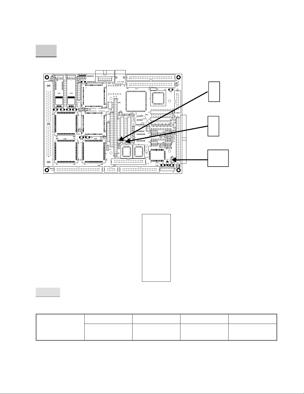
2.3 CPU Speed Se lec tion
J36
1 2 3
o o o
J31
1 o
2 o
3 o
J12
1 o o 2
3 o o 4
5 o o 6
J14
1 o
2 o
3 o
The LBC- Plus uses a Crys tal con trolled fre quency syn the sizer to con trol the CPU clock rate. The
jumper block at J12 al lows for the se lec tion of any of 8 CPU base clock fre quen cies rang ing f rom 8
MHz to 100 MHz.
The ta ble be low gives all of the pos si ble CPU clock speeds avail able by jump er ing J12.
CPU
Speed
J12
1-2
J12
3-4
J12
5-6
8 Mhz ON ON ON
16 MHz ON ON OFF
33 MHz ON OFF ON
40 MHz ON OFF OFF
50 MHz OFF ON ON
66 MHz OFF ON OFF
80 MHz OFF OFF ON
100 MHz OFF OFF OFF
NOTE : The LBC- Plus board will be jumpered at the fac tory for the rated speed of the in stalled
proc es sor. Jump er ing J12 to any speed in ex cess of the rated speed may re sult in CPU over hea t ing,
misop era tion, and pos si ble de struc tion of the CPU. Fail ures of CPUs which have been op er at ed above
their rated speed or tem pera ture are not cov ered un der the Win Sys tems stan dard prod uct war ranty.
Page 2 - 2 OPERATIONS MANUAL LBC-Plus 991206

WinSystems - "The Embedded Systems Authority"
2.3.1 Clock Mul ti plier Se lect
486DX4 and 5X86 proc es sors ac tu ally run at a mul ti ple of the base os cil la tor fre quency. T he
jumper block at J36 al lows se lec tion of the mul ti plier as shown here :
J36
1 2 3
o o o
3X
J36
1 2 3
o o o
2X - 486
4X - 5X86
2.4 PCI Clock Se lect
The PCI bus clock source must be se lected us ing jumper blocks at J14 and J31. The CPUCLK
source may be se lected any time the CPU base fre quency is less than or equal to 33MHz. For any C PU
base fre quency in ex cess of 33MHz the CPUCLK/2 se lec tion must be made.
J14 J14
1 o
2 o
3 o
J31
1 o
2 o
3 o
1 o
2 o
3 o
CPUCLK
CPUCLK/2
J31
1 o
2 o
3 o
2.5 Mem ory In stal la tion
The LBC-Plus util izes user instal la ble 72- pin stan dard SIMMs. SIMM mod ules should be a
minimum speed of 70nS and X32 ar chi tec ture is pre ferred as there is no sup port for the par ity bits pro vided by X36 bit mod ules. A sin gle SIMM socket is pro vided which can sup port DRAM sizes from
1MB to 32MB.
In stal la tion is ac com plished with power off by an gling the SIMM mod ule ap proxi mately 30 de grees from ver ti cal and in sert ing the fin gers into the con nec tor (It may be nec es sary to r e move any de vice in stalled in the U27 socket. ). The SIMM mod ule is keyed slightly off- center and can not be in serted
back wards with out ex treme force. Once the fin gers are in the socket, the mod ule is then ro tat ed to the
ver ti cal un til the re tain ing clips snap into place. Re moval is the re verse pro cess. Pull th e re tain ing clips
out ward and the SIMM mod ule, once re leased, should ro tate back to an ap pro pri ate re moval an gle.
991206 OPERATIONS MANUAL LBC-Plus Page 2 - 3

WinSystems - "The Embedded Systems Authority"
2.6 In ter rupt rout ing
J30
1 o o 2
3 o o 4
5 o o 6
7 o o 8
9 o o 10
11 o o 12
13 o o 14
15 o o 16
17 o o 18
19 o o 20
21 o o 22
All in ter rupts on the LBC-Plus are routed to their re spec tive PC/104 bus pins. On board pe riph er als,
se rial, par al lel, and disk are routed to their typi cal us age in ter rupts us ing the jumper bl ock at J30. This
block al lows dis con nect ing or re rout ing of the on board in ter rupts. The lay out for the J30 header and the
de fault jumper set tings are shown here.
J30
IDE
LPT
1 o o 2
3 o o 4
5 o o 6
7 o o 8
9 o o 10
11 o o 12
13 o o 14
15 o o 16
17 o o 18
19 o o 20
21 o o 22
IRQ9
IRQ10
IEQ11
IRQ12
IRQ15
IRQ14
IRQ7
IRQ6
IRQ5
IRQ4
IRQ3
COM4
ENET
COM3
COM4
WS16C48
FLOPPY
COM3
COM1
COM2
Page 2 - 4 OPERATIONS MANUAL LBC-Plus 991206

WinSystems - "The Embedded Systems Authority"
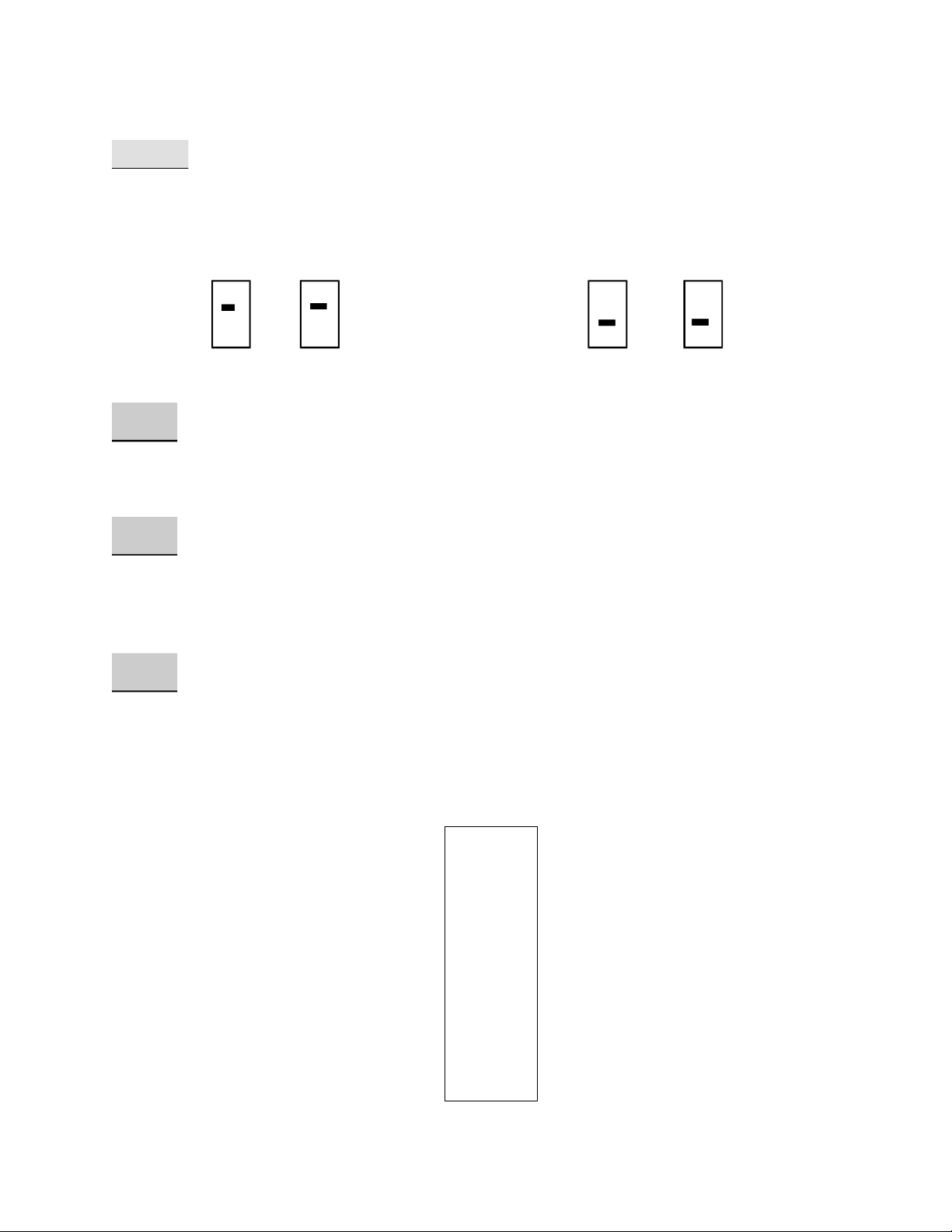
2.7 Real Time Clock/Cal en dar
J13
1 2 3
o o o
The LBC- Plus con tains an on board Clock/Cal en dar within the ALI1487 chip. This clock is fully
com pati ble with the MC146818A used in the origi nal PC- AT com put ers. This clock has a number o f
fea tures in clud ing pe ri odic and alarm in ter rupt ca pa bili ties. In ad di tion to the time a nd date keep ing
func tions, the sys tem con figu ra tion is kept within the CMOS RAM con tained in the clock sec ti on. This
RAM holds all of the setup in for ma tion re gard ing hard and floppy disk types, video type, shad owing,
wait states, etc. Ref er to the sec tion on the AWARD BIOS Setup for what is con fig ured via the C MOS
RAM.
It may be come nec es sary at some time to make the CMOS RAM for get its cur rent con figu ra tion and
to start fresh with fac tory de faults. This may be ac com plished by re mov ing power from the boa rd . Then
re move the jumper from pins 1-2 on J13 and place on pins 2-3 for 30 seconds. Re place the jumper o n
J13 pins 1-2, power- up, and re con fig ure the CMOS set tings as de sired.
NOTE : J13 is the mas ter bat tery en able jumper. Re mov ing the jumper re moves bat tery power from
the en tire board in clud ing the SSD ar ray. Be sure that any data con tained in bat tery backed S RAM is
backed up bef ore re mov ing the bat tery jumper. J13 must be jumpered 2-3 in the clear po si tion if a bat tery is not installed.
2.8 Key board In ter face
The LBC-Plus con tains an on board PC- AT style key board con trol ler. Key board con nec tion is
made through the Multi-I/O con nec tor at J3. An adapter ca ble P/N CBL- 162-1 is avail able from W in Sys tems to make ready ac cess to all of the de vices ter mi nated at the Multi-I/O con nec tor. Us ers de sir ing
cus tom con nec tions should ref er to the Multi-I/O con nec tor pin defi ni tions given later in t his man ual.
991206 OPERATIONS MANUAL LBC-Plus Page 2 - 5

WinSystems - "The Embedded Systems Authority"
2.9 Se rial In ter face
U8
J10
U9
J11
U3
1 2 3
o o o
J8
U5
1 2 3
o o o
U4
1 2 3
o o o
U6
J9
The LBC-Plus pro vides four 16550 com pati ble RS- 232 se rial ports at the fol low ing ad dresses :
COM1 3F8H at IRQ 4
COM2 2F8H at IRQ 3
COM3 3E8H* at IRQ 5**
COM4 2E8H* at IRQ 9**
*COM ports 3 and 4 can be en abled or dis abled in di vidu ally via the jumper block at J23. When J 23
pins 1-2 are jumpered, COM3 is en abled. When J23 pins 3-4 are jumpered, COM4 is en abled.
**The in ter rupts are not dis con nected when COM3 or COM4 are dis abled. Use the in ter rupt rout ing block de scribed ear lier to dis con nect the de fault in ter rupts if de sired.
1 2 3
o o o
Page 2 - 6 OPERATIONS MANUAL LBC-Plus 991206

WinSystems - "The Embedded Systems Authority"
The two pri mary se rial ports, COM1 and COM2 are con fig ur able for RS- 422, RS- 485 or J1708,
with the ad di tion of op tional driver ICs. The con figu ra tion op tions for each of the sup port ed modes are
shown on the fol low ing pages.
COM1 - RS- 232
COM1 DB9
J8 J10
1 2 3
o o o
1 2 3
o o o
U3 - In stalled
U4 - Not In stalled
U8 - Not In stalled
RX Data
TX Data
GND
CD
DTR
1 o o 6
2 o o 7
3 o o 8
4 o o 9
5 o
DSR
RTS
CTS
RI
COM2 - RS- 232
COM2 DB9
J9 J11
1 2 3
o o o
1 2 3
o o o
U5 - In stalled
U6 - Not In stalled
U9 - Not In stalled
RX Data
TX Data
DTR
GND
CD
1 o o 6
2 o o 7
3 o o 8
4 o o 9
5 o
DSR
RTS
CTS
RI
COM3/COM4 - RS- 232
COM3 and COM4 are RS- 232 only and are ter mi nated at J2. An adapter ca ble is avail able from
Win Sys tems ( P/N CBL- 173-1), which adapts J2 to two stan dard DB9M con nec tors. The pin defi ni tions for J2 are shown here :
J2
COM3 DCD
COM3 RX
COM3 TX
COM3 DTR
GND
COM4 DCD
COM4 RX
COM4 TX
COM4 DTR
GND
991206 OPERATIONS MANUAL LBC-Plus Page 2 - 7
1 o o 2
3 o o 4
5 o o 6
7 o o 8
9 o o 10
11 o o 12
13 o o 14
15 o o 16
17 o o 18
19 o o 20
COM3 DSR
COM3 RTS
COM3 CTR
COM3 RI
N/C
COM4 DSR
COM4 RTS
COM4 CTS
COM4 RI
N.C

WinSystems - "The Embedded Systems Authority"
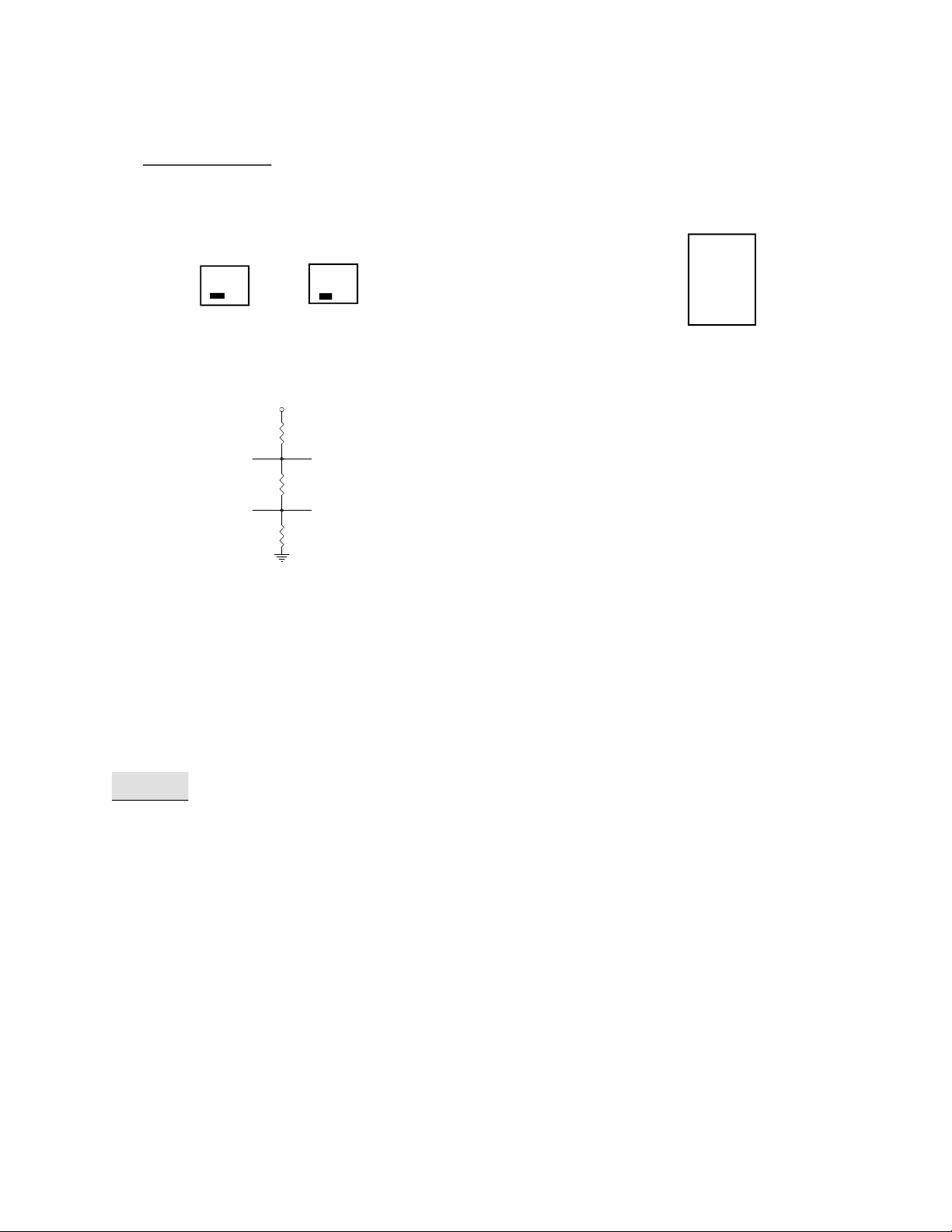
2.9.1 RS- 422 Mode Con figu ra tion
RS- 422 lev els are sup ported on both COM1 and COM2 with the in stal la tion of the op tional “Chi p
Kit”, Win Sys tems part number CK- 75176-2. This kit pro vides the driver ICs nec es sary for a sin gle
chan nel of RS- 422. If two chan nels of RS- 422 are re quired then two kits will be needed. RS- 42 2 is a 4 wire point-to-point full- duplex in ter face al low ing much longer ca ble runs than are pos si bl e with RS-
232. The dif fer en tial trans mit ter and re ceiver twisted pairs of fer a high de gree of noise im mu nity. RS 422 usu ally re quires the lines be ter mi nated at both ends. This ter mi na tion can be ac com p lished ei ther
on the ca ble or by in stall ing re sist ers on the board in lo ca tions re served for them. The me thod for de ter min ing the cor rect re sis tor val ues is be yond the scope of this docu ment but it is rec om men ded that trial
val ues of 100 ohms be used in all three lo ca tions at the re ceiver end. The fol low ing il lus t ra tion shows
the cor rect mode jump er ing, driver IC in stal la tion, I/O con nec tor pin defi ni tions, and te r mi na tion re sis tor lo ca tions for each of the chan nels when used in RS- 422 mode.
COM1 - RS- 422
COM1 DB9
J8 J10
1 2 3
o o o
VCC
R8
R9
R10
1 2 3
o o o
RX+
RX-
U3 - Not In stalled
U4 - In stalled
U8 - In stalled
RS- 422 NOTE : When used in RS- 422 mode,
the trans mit ter must be en abled by set ting the RTS
bit in the Mo dem Con trol Reg is ter (Bit1).
N/C
TX+
TX-
N/C
GND
1 o o 6
2 o o 7
3 o o 8
4 o o 9
5 o
RX+
RXN/C
N/C
Page 2 - 8 OPERATIONS MANUAL LBC-Plus 991206
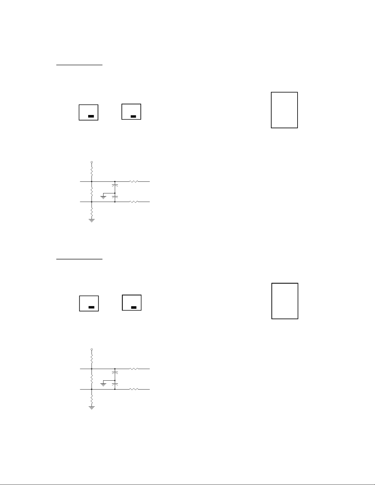
COM2 - RS- 422
WinSystems - "The Embedded Systems Authority"
COM2 DB9
J9 J11
1 2 3
o o o
1 2 3
o o o
U5 - Not In stalled
U6 - In stalled
U9 - In stalled
N/C
TX+
TX-
N/C
GND
1 o o 6
2 o o 7
3 o o 8
4 o o 9
5 o
RX+
RXN/C
N/C
RS- 422 NOTE : When used in RS- 422 mode,
VCC
R7
RX+
R6
RX-
R3
the trans mit ter must be en abled by set ting the RTS
bit in the Mo dem Con trol Reg is ter (Bit1).
2.9.2 RS- 485 Mode Con figu ra tion
The RS- 485 Multi- drop in ter face is sup ported on both chan nels with the in stal la tion of the op tional
“Chip Kit”, Win Sys tems part number CK- 75176-2. A sin gle kit is suf fi cient to con fig ure both chan nels
for RS- 485. RS- 485 is a 2- wire multi- drop in ter face where only one sta tion at a time talks ( trans mits)
while all oth ers lis ten (re ceive). RS- 485 usu ally re quires the twisted pair be ter mi nated a t each end of
the run. The re quired ter mi na tion val ues are de pend ent upon a number of fac tors in clud ing : line im ped ance, line length, etc. A good trial value is 100 ohms in all three re sis tor lo ca tions. The fol low ing il lus tra tions show the cor rect jump er ing, driver IC in stal la tion, I/O con nec tor pin out, and te r mi na tion
re sis tor lo ca tions for each of the chan nels when used in RS- 485 mode.
991206 OPERATIONS MANUAL LBC-Plus Page 2 - 9
COM1 - RS- 485
WinSystems - "The Embedded Systems Authority"
COM1 DB9
J8 J10
1 2 3
o o o
VCC
R8
R9
R10
1 2 3
o o o
TX/RX-
TX/RX+
U3 - Not In stalled
U4 - In stalled
U8 - Not In stalled
N/C
TX/RX+
TX/RX-
N/C
GND
1 o o 6
2 o o 7
3 o o 8
4 o o 9
5 o
N/C
N/C
N/C
N/C
RS- 485 NOTE : Be cause RS- 485 uses a sin gle
twisted- pair, all trans mit ters are con nected in par al lel. Only one sta tion at a time may trans mit or have
its trans mit ter en abled. The trans mit ter En able/Dis able is con trolled in soft ware us ing bit 1 in the Mo dem Con trol Reg is ter (RTS). When RTS is set, the
trans mit ter is en abled, and when cleared (the nor mal
state) the trans mit ter is dis abled and the re ceiver is
en abled. Note that it is nec es sary to al low some
mini mal set tling time af ter ena bling the trans mit ter
bef ore trans mit ting the first char ac ter. Like wise, fol low ing a trans mis sion, it is nec es sary to be sure that
all char ac ters have been com pletely shifted out of
the UART (Check Bit 6 in the Line Status Reg is ter)
bef ore dis abling the trans mit ter to avoid chop ping
off the last char ac ter.
Page 2 - 10 OPERATIONS MANUAL LBC-Plus 991206
COM2 - RS- 485
WinSystems - "The Embedded Systems Authority"
COM2 DB9
J9 J11
1 2 3
o o o
VCC
R14
R15
R16
1 2 3
o o o
TX/RX-
TX/RX+
U5 - Not In stalled
U6 - In stalled
U9 - Not In stalled
N/C
TX/RX+
TX/RX-
N/C
GND
1 o o 6
2 o o 7
3 o o 8
4 o o 9
5 o
N/C
N/C
N/C
N/C
RS- 485 NOTE : Be cause RS- 485 uses a sin gle
twisted- pair, all trans mit ters are con nected in par al lel. Only one sta tion at a time may trans mit or have
its trans mit ter en abled. The trans mit ter En able/Dis able is con trolled in soft ware us ing bit 1 in the Mo dem Con trol Reg is ter (RTS). When RTS is set, the
trans mit ter is en abled, and when cleared (the nor mal
state) the trans mit ter is dis abled and the re ceiver is
en abled. Note that it is nec es sary to al low some
mini mal set tling time af ter ena bling the trans mit ter
bef ore trans mit ting the first char ac ter. Like wise, fol low ing a trans mis sion, it is nec es sary to be sure that
all char ac ters have been com pletely shifted out of
the UART (Check Bit 6 in the Line Status Reg is ter)
bef ore dis abling the trans mit ter to avoid chop ping
off the last char ac ter.
2.9.3 SAE J1708 Con figu ra tion
The So ci ety of Auto mo tive En gi neers (SAE) J1708 in ter face is a varia tion of the RS- 485 in ter face
which is used for “Se rial Data Com mu ni ca tions be tween Mi cro com puter Sys tems in Heavy Duty Ve hi cle Ap pli ca tions”. It is be yond the scope of this docu ment to go into de tail on the J1708 spe ci fi ca tion.
The LBC- Plus may be user con fig ured for J1708 by the ad di tion of the CK- 75176-2 “Chip Kit”. O ne
“Chip Kit” is suf fi cient to con fig ure both chan nels for J1708. The il lus tra tions that fol l ow show the cor rect jump er ing, driver IC in stal la tion, I/O con nec tor pin defi ni tions, and the ter mi na t ion net work de tails
for each of the chan nels when used in J1708 mode.
991206 OPERATIONS MANUAL LBC-Plus Page 2 - 11
COM1 - J1708
WinSystems - "The Embedded Systems Authority"
COM1 DB9
J8 J10
1 2 3
o o o
VCC
R11
4.7K
R12
Absent
R13
4.7K
COM2 - J1708
1 2 3
o o o
R1 470 OHM
C1 .0022 ufd
C2 .0022 ufd
R2 470 OHM
U3 - Not In stalled
U4 - In stalled
U8 - Not In stalled
TX/RX+
TX/RX-
N/C
TX/RX+
TX/RX-
N/C
GND
1 o o 6
2 o o 7
3 o o 8
4 o o 9
5 o
N/C
N/C
N/C
N/C
R14
4.7K
R15
Absent
R16
4.7K
J9 J11
1 2 3
o o o
VCC
1 2 3
o o o
R5 470 OHM
C4 .0022 ufd
C3 .0022 ufd
R4 470 OHM
U5 - Not In stalled
U6 - In stalled
U9 - Not In stalled
TX/RX+
TX/RX-
N/C
TX/RX+
TX/RX-
N/C
GND
COM2 DB9
1 o o 6
2 o o 7
3 o o 8
4 o o 9
5 o
N/C
N/C
N/C
N/C
Page 2 - 12 OPERATIONS MANUAL LBC-Plus 991206
WinSystems - "The Embedded Systems Authority"
2.10 Par al lel Printer Port
J24
1 2
o o
o o
3 4
J21
1 2
o o
o o
3 4
J6
1 o o 2
3 o o 4
5 o o 6
The LBC- Plus sup ports a fully bi- directional par al lel printer port ca pa ble of EPP and ECP op era tions. The par al lel port is mapped at 278H and is ter mi nated at the Multi-I/O con nec tor J3. T he pin defi ni tions for the par al lel port DB25 con nec tor when us ing the CBL- 162-1 cable are shown be low :
PD0
PD1
PD2
PD3
PD4
PD5
PD6
PD7
ACK
PE
SLCT
1 o o 14
2 o o 15
3 o o 16
4 o o 17
5 o o 18
6 o o 19
7 o o 20
8 o o 21
9 o o 22
10 o o 23
11 o o 24
12 o o 25
13 o
AUTOFD
ERROR
INIT
SLIN
GND
GND
GND
GND
GND
GND
GND
GND
STROBE
BUSY
2.10.1 Par al lel Port Mode Se lec tion
The par al lel port mode is se lected via the jumper block at J6 per the fol low ing ta ble :
SPP Mode EPP Mode ECP Mode EPP/ECP Mode
J6
Jumpering
3-5
4-6
3-5
2-4
1-3
4-6
1-3
2-4
991206 OPERATIONS MANUAL LBC-Plus Page 2 - 13
WinSystems - "The Embedded Systems Authority"
2.10.2 ECP DMA Con figu ra tion
When the par al lel port is used in an ECP con figu ra tion, the jumper blocks at J21 and J24 are u sed to
se lect the de sired DMA chan nel as shown here :
J21 J24
1 2
o o
o o
3 4
DMA Chan nel 1 DMA Chan nel 3
1 2
o o
o o
3 4
J21
1 2
o o
o o
3 4
J24
1 2
o o
o o
3 4
2.11 Speaker/Sound In ter face
The LBC- Plus util izes a high- impedance piezo type de vice for audio out put. BIOS beep codes, er ror sig nal ing, or user de fined tones can be pre sented via this de vice.
2.12 PC/104 Bus In ter face
The LBC- Plus sup ports I/O ex pan sion through the stan dard PC/104 con nec tors at J26 and J29. T he
LBC- Plus sup ports both 8- bit and 16- bit PC/104 mod ules. The PC/104 con nec tor pin defi ni tio ns are
pro vided on the fol low ing page for ref er ence pur poses.
2.13 Floppy Disk In ter face
The LBC- Plus sup ports up to 2 stan dard 3 1/2" or 5 1/4" PC com pati ble floppy disk drives. The
drives are con nected via the I/O con nec tor at J17. Note that the in ter con nect ca ble to the d rives is a stan dard floppy I/O ca ble used on desk- top PCs. The ca ble must have the twisted sec tion prior to t he drive A
po si tion. The pin defi ni tions for the J17 con nec tor are shown here :
J17
GND
1 o o 2
3 o o 4
GND
5 o o 6
GND
GND
7 o o 8
9 o o 10
GND
11 o o 12
GND
GND
13 o o 14
15 o o 16
GND
17 o o 18
GND
GND
19 o o 20
21 o o 22
GND
23 o o 24
GND
GND
25 o o 26
27 o o 28
GND
29 o o 30
GND
GND
31 o o 32
33 o o 34
GND
Page 2 - 14 OPERATIONS MANUAL LBC-Plus 991206
RPM/LC
N/C
N/C
INDEX
MTR0
DRV1
DRV0
MTR1
DIR
STEP
WDATA
WGATE
TRK0
WPRT
RDATA
HDSEL
DSKCHG

WinSystems - "The Embedded Systems Authority"
GND
RESET
+5V
IRQ9
-5V
DRQ2
-12V
0WS
+12V
GND
MEMW
MEMR
IOW
IOR
DACK3
DRQ3
DACK1
DRQ1
REFRESH
SYSCLK
IRQ7
IRQ6
IRQ5
IRQ4
IRQ3
DACK2
TC
BALE
+5V
OSC
GND
GND
J26
B1 o o A1
B2 o o A2
B3 o o A3
B4 o o A4
B5 o o A5
B6 o o A6
B7 o o A7
B8 o o A8
B9 o o A9
B10 o o A10
B11 o o A11
B12 o o A12
B13 o o A13
B14 o o A14
B15 o o A15
B16 o o A16
B17 o o A17
B18 o o A18
B19 o o A19
B20 o o A20
B21 o o A21
B22 o o A22
B23 o o A23
B24 o o A24
B25 o o A25
B26 o o A26
B27 o o A27
B28 o o A28
B29 o o A29
B30 o o A30
B31 o o A31
B32 o o A32
IOCHK
BD7
BD6
BD5
BD4
BD3
BD2
BD1
BD0
IOCHRDY
AEN
SA19
SA18
SA17
SA16
SA15
SA14
SA13
SA12
SA11
SA10
SA9
SA8
SA7
SA6
SA5
SA4
SA3
SA2
SA1
SA0
GND
GND
SBHE
LA23
LA22
LA21
LA20
LA19
LA18
LA17
MEMR
MEMW
SD8
SD9
SD10
SD11
SD12
SD13
SD14
SD15
KEY
J29
C0 o o D0
C1 o o D1
C2 o o D2
C3 o o D3
C4 o o D4
C5 o o D5
C6 o o D6
C7 o o D7
C8 o o D8
C9 o o D9
C10 o o D10
C11 o o D11
C12 o o D12
C13 o o D13
C14 o o D14
C15 o o D15
C16 o o D16
C17 o o D17
C18 o o D18
C19 o o D19
GND
MEMCS16
IOCS16
IRQ10
IRQ11
IRQ12
IRQ15
IRQ14
DACK0
DRQ0
DACK5
DRQ5
DACK6
DRQ6
DACK7
DRQ7
VCC
MASTER
GND
GND
991206 OPERATIONS MANUAL LBC-Plus Page 2 - 15

WinSystems - "The Embedded Systems Authority"
2.14 IDE Hard Disk In ter face
The LBC-Plus sup ports stan dard IDE fixed disks through the I/O con nec tor at J18. A red ac tiv i ty
LED is pres ent at D1. The pin defi ni tions for J18 are shown here :
J18
D7
D6
D5
D4
D3
D2
D1
D0
GND
GND
IOW
IOR
N/C
N/C
A1
A0
N/C
1 o o 2
3 o o 4
5 o o 6
7 o o 8
9 o o 10
11 o o 12
13 o o 14
15 o o 16
17 o o 18
19 o o 20
21 o o 22
23 o o 24
25 o o 26
27 o o 28
29 o o 30
31 o o 32
33 o o 34
35 o o 36
37 o o 38
39 o o 40
GND
D8
D9
D10
D11
D12
D13
D14
D15
N/C
GND
GND
GND
ALE
GND
IOCS16
N/C
A2
HDCS1
GND
RESET
INTRQ
HDCS0
2.15 Watch dog Timer Con figu ra tion
The LBC- Plus board fea tures a power- on volt age de tect and power- down/power brown- out re set
cir cuit to pro tect mem ory and I/O from faulty CPU op era tion dur ing pe ri ods of il le gal vol t age lev els.
This su per vi sor cir cuitry also fea tures a watch dog timer which can be used to guard against s oft ware
lock ups. An in ter nal timer with a pe ri od of 1.5 sec onds will, when en abled, re set the CPU i f the watch dog has not been serv iced within the al lot ted time. There are three watch dog modes avail able o n the
LBC- Plus. With no jumper in stalled on J19, the watch dog is to tally dis abled and can never re s et the
CPU. When J19 is jumpered on pins 2-3, the watch dog cir cuit is per ma nently en abled and tim ing be gins im me di ate ly with power- on. This mode is NOT com pati ble with the AWARD BIOS or with MS DOS but is avail able for di rectly em bed ded code that takes the place of the BIOS. The watch do g must
be ac cessed every 1.5 sec onds or a re set will oc cur. Pet ting in this mode is ac com plished by writ ing to
I/O port 1EFH with any value.
An al ter nate mode of op era tion is via soft ware en able/dis able con trol. This mode is set by jump er ing J19 pins 1-2. In this mode the watch dog timer powers- up dis abled and must be en abled in sof t ware
bef ore tim ing will be gin. Ena bling is ac com plished by writ ing a 1 to I/O port 1EEH. Writ in g a 0 to I/O
port 1EEH will dis able the watch dog. Af ter ena bling, pet ting may be ac com plished by writ ing any
value to I/O port 1EFH at least every 1.5 sec onds or a re set will oc cur. This mode of op era tio n can be
used with the BIOS or DOS pro vided that the watch dog is dis abled bef ore mak ing any ex ten sive BIOS
or DOS calls, es pe cially video or Disk IO calls which could ex ceed the 1.5 sec onds al lowed. Th e draw -
Page 2 - 16 OPERATIONS MANUAL LBC-Plus 991206
WinSystems - "The Embedded Systems Authority"
back to this mode is that a lockup dur ing the time the watch dog is dis abled will not al low for auto recovery and will re quire an ex ter nal re set.
J13
1 2 3
o o o
J19
1 2 3
o o o
2.16 Status LED
A green LED is popu lated on the board at D2 which can be used for any ap pli ca tion spe cific pur pose. The LED can be turned on in soft ware by writ ing a 1 to I/O port 1EDH. The LED can be turned off
by writ ing a 0 to 1EDH.
2.17 Bat tery Se lect Con trol
An on board 200mAh nomi nal ca pac ity, lith ium coin- cell bat tery is pro vided for the CMOS
Clock/Cal en dar and for bat tery backing- up Solid State Disk SRAMs. A mas ter bat tery en able j umper is
pro vided at J13. When J13 is jumpered pins 1-2, bat tery power is sup plied to the Clock/Cal en da r and to
the in di vid ual jumper blocks for bat tery backup of SSD SRAMs. When J13 is jumpered pins 2-3, th e
bat tery is to tally dis con nected and no cur rent will be drawn from it. Bat tery life is highly de pend ent
upon duty cy cle as there is no cur rent drawn from the bat tery when +5 volts is ap plied to the b oard. Both
stor age and op era tional tem pera tures play a promi nent fac tor in bat tery life. High tem pera tures will
shorten bat tery life sig nifi cantly. J13 must be jumpered 2-3 in the clear po si tion if a bat te ry is not
installed.
991206 OPERATIONS MANUAL LBC-Plus Page 2 - 17
WinSystems - "The Embedded Systems Authority"
2.18 Power/Re set Con nec tion
Power is sup plied to the LBC-Plus via the con nec tor at J7. The pin defi ni tions for J7 are give n be low. An op tional normally- open push- button- reset switch may also be con nected to J7 be tween P BRE SET* and ground.
J7
8 o
7 o
6 o
5 o
4 o
3 o
2 o
1 o
PBRESET*
GND
GND
GND
+5V
+5V
+12V
-12V
2.19 Sili con Disk Con figu ra tion
J38
2 4 6 8 10
o o o o o
o o o o o
1 3 5 7 9
J40
1 o
2 o
3 o
J34
1 o
2 o
3 o
J16
1 o
J39
2 4 6 8 10
o o o o o
o o o o o
1 3 5 7 9
2 o
3 o
J25
1 o
2 o
The LBC- Plus sup ports the use of EPROM, PEROM (Flash), SRAM, and the M- Systems Disk On Chip (DOC) de vices to be used as Solid State Disk (SSD) drives. Sec tion 4 of this man ual pro vi des the
nec es sary in for ma tion for the gen era tion and us age of the Sili con drives. This sec tion do cu ments the re quired hard ware con figu ra tions for the vari ous type of de vices. Two 32- pin JE DEC mem ory so ck ets at
U27 and U23 are used to con tain the RAM, ROM,Flash, or DOC de vices used for the disk. The sili co n
Page 2 - 18 OPERATIONS MANUAL LBC-Plus 991206

WinSystems - "The Embedded Systems Authority"
disk ar ray is mem ory mapped into a 16k byte hole at seg ment E400H and has an I/O con trol reg i s ter at
1ECH.
2.19.1 Sili con Disk Mode
There are two ba sic modes of Sili con Disk op era tion on the LBC- Plus. The first uses the on boa rd
BIOS ex ten sion and sup ports the use of 512K or 1M EPROMS, 512K SRAMS, or 512K AT MEL Flash
De vices. The sec ond mode uses the M- Systems Disk On Chip de vice. The mode is con trolled via th e
jumper block at J25 as shown here :
J25
1 o
2 o
DOC Mode
J25
1 o
2 o
SSD Mode
NOTE : Jump er ing for DOC mode with EPROMs, RAMs, of Flash de vices in stalled ef fec tively
acts as a dis able to the Solid State Disk and simi larly when a DOC de vice is in stalled and the jumper is
se lected for stan dard de vices the DOC is dis abled.
IM POR TANT NOTE : To in sure Win dows 95 com pati bil ity, J25 must be jumpered 1-2.
2.19.2 De vice Size Se lec tion
The on board Solid State Disk ar ray sup ports ei ther 512K EPROMs, SRAMs or FLASH de vice or
1M EPROM de vices. The de vice size se lec tion is made at J16 as shown here :
J16
1 o
2 o
3 o
J16
1 o
2 o
3 o
512K or DOC Device
991206 OPERATIONS MANUAL LBC-Plus Page 2 - 19
1M Devices

WinSystems - "The Embedded Systems Authority"
2.19.3 De vice Type Se lec tion
Each of the de vices in the ar ray has an in di vid ual de vice type jumper block at the de vice so cket. J39
sets the de vice type for U27 and J38 sets the de vice type for U23. The sup ported de vice type ju mp er ings
are shown here :
2 4 6 8 10
o o o o o
o o o o o
1 3 5 7 9
512K X 8
SRAM
2 4 6 8 10
o o o o o
o o o o o
1 3 5 7 9
512K X 8
EPROM
2 4 6 8 10
o o o o o
o o o o o
1 3 5 7 9
512K X 8
PEROM
2 4 6 8 10
o o o o o
o o o o o
1 3 5 7 9
1 MEG X 8
EPROM
2 4 6 8 10
o o o o o
o o o o o
1 3 5 7 9
DOC
DEVICE
2.19.4 Bat tery Backup Se lec tion
When us ing SRAM de vices and non vola tile op era tion is de sired, bat tery backup can be se lect ed on
a socket- by- socket ba sis. J40 for U27 and J34 for U23. The il lus tra tion be low shows the jump er ing for
bat tery backup or stan dard op era tion.
1 o
2 o
3 o
Bat tery Backup
Enabled
1 o
2 o
3 o
Bat tery Backup
Disabled
NOTE : Hav ing the jumper(s) se lected for bat tery backup when us ing other than low- power standby SRAMs (such as with EPROMs, or PEROMs) will re sult in the quick drain ing of the on board
bat tery.
2.19.5 Sili con Disk Notes
1. When in stall ing de vices, U27 is the first de vice in the ar ray and must al ways con tain the first de -
vice of a boota ble disk.
2. The Disk On Chip op tion must use the socket at U23. When a DOC is in stalled, U27 is avail abl e
as a Sec ondary Sili con Disk de vice. See sec tion 4.4 for more in for ma tion.
Page 2 - 20 OPERATIONS MANUAL LBC-Plus 991206

WinSystems - "The Embedded Systems Authority"
2.20 Par al lel I/O
The LBC-Plus util izes the Win Sys tems WS16C48 ASIC high- density I/O chip mapped at a base
ad dress of 120H. The first 24 lines are ca pa ble of fully latched event sens ing with sense po la r ity be ing
soft ware pro gram ma ble. Two 50- pin con nec tors al low for easy mat ing with in dus try stan da rd I/O
racks.
J1
1 o
2 o
J15
1 o
2 o
2.20.1 Par al lel I/O En able
The par al lel fea tures of the LBC- Plus can be en abled or dis abled us ing the jumper block at J 15.
When J15 is jumpered the par al lel I/O is en abled at I/O ad dress 120H. When J15 is open the 16 a d dresses start ing at I/O ad dress 120H are free for use by other de vices.
2.20.2 Par al lel I/O Con nec tors
The 48 lines of par al lel I/O are ter mi nated through two 50- pin con nec tors at J4 and J5. The J4 con nec tor han dles I/O ports 0-2 while J5 han dles ports 3-5. The pin defi ni tions for J4 and J5 are shown on
the fol low ing page.
991206 OPERATIONS MANUAL LBC-Plus Page 2 - 21

WinSystems - "The Embedded Systems Authority"
Port 2 Bit 7
Port 2 Bit 6
Port 2 Bit 5
Port 2 Bit 4
Port 2 Bit 3
Port 2 Bit 2
Port 2 Bit 1
Port 2 Bit 0
Port 1 Bit 7
Port 1 Bit 6
Port 1 Bit 5
Port 1 Bit 4
Port 1 Bit 3
Port 1 Bit 2
Port 1 Bit 1
Port 1 Bit 0
Port 0 Bit 7
Port 0 Bit 6
Port 0 Bit 5
Port 0 Bit 4
Port 0 Bit 3
Port 0 Bit 2
Port 0 Bit 1
Port 0 Bit 0
+5V
J4
1 o o 2
3 o o 4
5 o o 6
7 o o 8
9 o o 10
11 o o 12
13 o o 14
15 o o 16
17 o o 18
19 o o 20
21 o o 22
23 o o 24
25 o o 26
27 o o 28
29 o o 30
31 o o 32
33 o o 34
35 o o 36
37 o o 38
39 o o 40
41 o o 42
43 o o 44
45 o o 46
47 o o 48
49 o o 50
GND
GND
GND
GND
GND
GND
GND
GND
GND
GND
GND
GND
GND
GND
GND
GND
GND
GND
GND
GND
GND
GND
GND
GND
GND
Port 5 Bit 7
Port 5 Bit 6
Port 5 Bit 5
Port 5 Bit 4
Port 5 Bit 3
Port 5 Bit 2
Port 5 Bit 1
Port 5 Bit 0
Port 4 Bit 7
Port 4 Bit 6
Port 4 Bit 5
Port 4 Bit 4
Port 4 Bit 3
Port 4 Bit 2
Port 4 Bit 1
Port 4 Bit 0
Port 3 Bit 7
Port 3 Bit 6
Port 3 Bit 5
Port 3 Bit 4
Port 3 Bit 3
Port 3 Bit 2
Port 3 Bit 1
Port 3 Bit 0
+5V
J5
1 o o 2
3 o o 4
5 o o 6
7 o o 8
9 o o 10
11 o o 12
13 o o 14
15 o o 16
17 o o 18
19 o o 20
21 o o 22
23 o o 24
25 o o 26
27 o o 28
29 o o 30
31 o o 32
33 o o 34
35 o o 36
37 o o 38
39 o o 40
41 o o 42
43 o o 44
45 o o 46
47 o o 48
49 o o 50
GND
GND
GND
GND
GND
GND
GND
GND
GND
GND
GND
GND
GND
GND
GND
GND
GND
GND
GND
GND
GND
GND
GND
GND
GND
2.20.3 Par al lel I/O VCC En able
The I/O con nec tors can pro vide +5 volts to an I/O rack or for mis cel la ne ous pur poses by jum p er ing
J1. When J1 is jumpered +5 volts is pro vided at pin 49 of both J4 and J5. It the user's re spon s i bil ity to
limit cur rent to a safe value (less than 1A) to avoid dam ag ing the CPU board.
2.20.4 WS16C48 Reg is ter Defi ni tions
The LBC- Plus uses the Win Sys tems’ ex clu sive ASIC de vice, the WS16C48. This de vice pro vides
48 lines of digi tal I/O. There are 17 unique reg is ters within the WS16C48. The fol low ing ta b le sum ma rizes the reg is ters and the text that fol lows pro vides de tails on each of the in ter nal reg i s ters.
Page 2 - 22 OPERATIONS MANUAL LBC-Plus 991206

WinSystems - "The Embedded Systems Authority"
I/O Ad dress
Offset
Page 0 Page 1 Page 2 Page 3
00H Port 0 I/O Port 0 I/O Port 0 I/O Port 0 I/O
01H Port 1 I/O Port 1 I/O Port 1 I/O Port 1 I/O
02H Port 2 I/O Port 2 I/O Port 2 I/O Port 2 I/O
03H Port 3 I/O Port 3 I/O Port 3 I/O Port 3 I/O
04H Port 4 I/O Port 4 I/O Port 4 I/O Port 4 I/O
05H Port 5 I/O Port 5 I/O Port 5 I/O Port 5 I/O
06H Int_Pending Int_Pending Int_Pending Int_Pending
07H Page/Lock Page/Lock Page/Lock Page/Lock
08H N/A Pol_0 Enab_0 Int_ID0
09H N/A Pol_1 Enab_1 Int_ID1
0AH N/A Pol_2 Enab_2 Int_ID2
Reg is ter De tails
Port 0-5 I/O - Each I/O bit in each of the 6 ports can be in di vidu ally pro grammed for in put or out -
put. Writ ing a '0' to a bit po si tion causes the cor re spond ing out put pin to go to a High- Im pedance state
(pulled high by ex ter nal 10K ohm re sis tors). This al lows it to be used as an in put. When used in the in put
mode, a read re flects the in verted state of the I/O pin, such that a high on the pin will read as a '0' in the
reg is ter. Writ ing a '1' to a bit po si tion causes the out put pin to sink cur rent (up to 12mA) , ef fec tively
pull ing it low.
INT_PEND ING - This read- only reg is ter re flects the com bined state of the INT_ID0 through
INT_ID2 reg is ters. When any of the lower 3 bits are set, it in di cates that an in ter rupt is pe nd ing on the
I/O port cor re spond ing to the bit po si tion(s) that are set. Read ing this reg is ter al lows a n In ter rupt Serv ice Rou tine to quickly de ter mine if any in ter rupts are pend ing and which I/O port has a pend ing in ter rupt.
PAGE/LOCK - This reg is ter serves two pur poses. The up per two bits se lect the reg is ter page in use
as shown here :
D7 D6 Page
0 0 Page 0
0 1 Page 1
1 0 Page 2
1 1 Page 3
991206 OPERATIONS MANUAL LBC-Plus Page 2 - 23

WinSystems - "The Embedded Systems Authority"
Bits 5-0 al low for lock ing the I/O ports. A '1' writ ten to the I/O port po si tion will pro hibi t fur ther
writes to the cor re spond ing I/O port.
POL0- POL2 - These reg is ters are ac ces si ble when page 1 is se lected. They al low in ter rupt po lar ity
se lec tion on a port- by- port and bit- by- bit ba sis. Writ ing a '1' to a bit po si tion se lect s the ris ing edge de tec tion in ter rupts while writ ing a '0' to a bit po si tion se lects fal ling edge de tec tion i n ter rupts.
ENAB0- ENAB2 - These reg is ters are ac ces si ble when page 2 is se lected. They al low for port- by port and bit- by- bit ena bling of the edge de tec tion in ter rupts. When set to a '1' the edge d e tec tion in ter rupt is en abled for the cor re spond ing port and bit. When cleared to a '0' the bit's edge de tec tion in ter rupt
is dis abled. Note that this reg is ter can be used to in di vidu ally clear a pend ing in ter rupt by dis abling and
reena bling the pend ing in ter rupt.
INT_ID0 - INT_ID2 - These reg is ters are ac ces si ble when page 3 is se lected. They are used to
iden tify cur rently pend ing edge in ter rupts. A bit when read as a '1' in di cates that an edge of the po lar ity
pro grammed into the cor re spond ing po lar ity reg is ter has been rec og nized. Note that a writ e to this reg is ter (value ig nored) clears ALL of the pend ing in ter rupts in this reg is ter.
2.21 VGA Con figu ra tion
J20
1 2
o o
o o
3 4
Page 2 - 24 OPERATIONS MANUAL LBC-Plus 991206

WinSystems - "The Embedded Systems Authority"
2.21.1 In tro duc tion
The LBC- Plus uses a third gen era tion CRT/Flat panel VGA con trol ler. It sup ports stan dard VGA
out put as well as a va ri ety of Flat Panel Dis plays us ing op tional Flat Panel Adapter (FPA) mo d ules. The
video on the LBC-Plus uses the Chips and Tech nolo gies 6554X se ries of high per form ance VGA co n trol lers. The C&T con trol ler sup ports stan dard and Super- VGA modes as well as Color and Mono chrome pan els with 8,9,12,15,16,18, and 24- bit in ter faces. Win Sys tems pro vides flat panel su p port
through a se ries of FPA (Flat Panel Adapter) mod ules. Con tact your Win Sys tems Ap pli ca tions En gi neer for the most cur rent list of avail able FPAs and sup ported pan els.
De tails re gard ing in ter fac ing to spe cific Flat Pan els is not pro vided in this man ual but should be ref er enced in the docu men ta tion ac com pa ny ing the FPA mod ule. At tempted con nec tion to any f lat panel
not di rectly sup ported by a Win Sys tems FPA mod ule is at the user's risk and ex treme care shou ld be ex er cised to avoid dam ag ing or de stroy ing the panel.
HAZ ARD WARN ING : LCD pan els can re quire a high volt age for the panel back light. This high frequency volt age can ex ceed 1000 volts and can pres ent a shock haz ard. Care should be taken w hen
wir ing or han dling the inverter out put. To avoid dan ger of shock and to avoid dam ag ing frag i le and ex pen sive pan els, make all con nec tion changes with power re moved.
2.21.2 VGA BIOS ROM Type Se lec tion
The LBC- Plus comes stan dard with a video BIOS ex pan sion ROM popu lated at U15. Vari ous
ROM sizes can be used to sup port a va ri ety of flat panel con figu ra tions each need ing its own BIOS im age. The FPA adapter mod ules, when con nected to J33, auto mati cally se lect the cor rect BIOS im age for
the panel fam ily the FPA sup ports. The fac tory will or di nar ily con fig ure the BIOS ROM for t he size
pro vided but the il lus tra tion be low shows the proper jump er ing of J20 for the sup ported RO M sizes.
J20
1 2
o o
o o
3 4
27C010
27C020
27C040
J20
1 2
o o
o o
3 4
27C080
991206 OPERATIONS MANUAL LBC-Plus Page 2 - 25

WinSystems - "The Embedded Systems Authority"
2.21.3 CRT Out put Con nec tion
Video out put to a stan dard VGA moni tor is made via the con nec tor at J27. An adapter ca ble par t
number CBL- 207-1 is avail able from Win Sys tems to adapt from J27 to the stan dard DB15 VGA con nec tor. The pin defi ni tions for the J27 con nec tor are shown here :
J27
RED
GREEN
BLUE
HSYNC
VSYNC
1 o o 2
3 o o 4
5 o o 6
7 o o 8
9 o o 10
GND
GND
GND
GND
GND
2.21.4 Flat Panel Out put Con nec tion
Con nec tion to all flat pan els is made via the 50- pin con nec tor at J33. This con nec tor is ca bled to the
ap pro pri ate FPA (Flat Panel Adapter) mod ule which then breaks out the nec es sary ca bling fo r at tach ment to the panel it self. The FPA mod ule also sup plies any spe cial con trols that may be needed for the
panel. Ref er to the FPA docu men ta tion for spe cific hook- up in struc tions. The pin defi ni ti ons for J33 are
shown here :
SW0
SW2
P23
P21
P19
GND
P17
P15
P13
GND
P11
P9
P7
GND
P5
P3
P1
GND
SHFCLK
FLM
ENVCC
ENVEE
PVS
+12V
VCC
J33
1 o o 2
3 o o 4
5 o o 6
7 o o 8
9 o o 10
11 o o 12
13 o o 14
15 o o 16
17 o o 18
19 o o 20
21 o o 22
23 o o 24
25 o o 26
27 o o 28
29 o o 30
31 o o 32
33 o o 34
35 o o 36
37 o o 38
39 o o 40
41 o o 42
43 o o 44
45 o o 46
47 o o 48
49 o o 50
SW1
SW3
P22
P20
P18
GND
P16
P14
P12
GND
P10
P8
P6
GND
P4
P2
P0
GND
LP
M
ENBKL
PHS
-12V
+12V
VCC
Page 2 - 26 OPERATIONS MANUAL LBC-Plus 991206

WinSystems - "The Embedded Systems Authority"
2.21.5 Video Mode Ta bles
The LBC- Plus video sec tion sup ports a number of stan dard and ex tended VGA modes. The fol low ing ta bles ex tracted from the C&T 65540/65545 da ta book show the video modes along with the re quired amount of RAM.
Stan dard Video Modes - VGA Stan dard
Mode
(Hex)
0+, 1+ Text
2+, 3+ Text 16
7+ Text Mono
10 Planar 16 80 X 25 8 X 14 640 X 350 25.175 31.5 70 256KB A,B,C
11 Planar 2 80 X 30 8 X 16 640 X 480 25/175 31.5 60 256KB A,B,C
12 Planar 16 80 X 30 8 X 16 640 X 480 25.175 31.5 60 256KB A,B,C
13
Dis play
#
Mode
Col ors
16
4 Graph ics 4 40 X 25 8 X 8 320 X 200 25.175 31.5 70 256KB A,B,C
5 Graphics 4 40 X 25 8 X 8 320 X 200 15.175 31.5 70 256KB A,B,C
6 Graphics 2 80 X 25 8 X 8 640 X 200 25.175 31.5 70 256KB A,B,C
D Planar 16 40 X 25 8 X 8 320 X 200 25.175 31.5 70 256KB A,B,C
E Planar 16 80 X 25 8 X 8 640 X 200 25.175 31.5 70 256KB A,B,C
F Planar Mono 80 X 25 8 X 14 640 X 350 25.175 31.5 70 256KB A,B,C
Packed
Pixel
256 40 X 25 8 X 8 320 X 200 25.175 31.5 70 256KB A,B,C
Text
Dis play
40 X 25
40 X 25
40 X 25
80 X 25
80 X 25
80 X 25
80 X25
80 X 25
80 X 25
Font
Size
9 X 16
8 X 14
8 X 8
9 X 16
8 X 14
8 X 8
9 X 16
9 X 14
9 X 8
Pixel
Reso lu tion
360 X 400
320 X 350
320 X 200
720 X 400
640 X 350
620 X 200
720 X 400
720 X 350
720 X 350
Dot
Clock
(MHz)
28.322
25.175
25.175
28.322
25.175
25.175
28.322 31.5 70 256KB A,B,C
Hori zon tal
Fre quency
(KHz)
31.5 70 256KB A,B,C
31.5 70 256KB A,B,C
Ver ti cal
Fre quency
(Hz)
Video
Memory
CODE
CRT
CRT Codes
A - PS/2 Fixed Frequency analog CRT or equivalent (31.5/35.5 Khz Horizontal Frequency Specification )
B - Multi-Frequency CRT Monitor (37.5 Khz minimum Horizontal Frequency Specification) (NEC MultiSyn c 3D or equivalent)
C - Multi-Frequency High-Performance CRT Monitor (48.5 KHZ minimum Horizontal Frequency Specificati on) MultiSyc 5D or equivalent
991206 OPERATIONS MANUAL LBC-Plus Page 2 - 27

WinSystems - "The Embedded Systems Authority"
Ex tended Reso lu tion Modes
Mode
#
(Hex)
Dis play
Mode
Col ors
Text
Dis play
Font
Size
Pixel
Reso lu tion
Dot
Clock
(MHz)
Hori zon tal
Fre quency
(KHz)
Ver ti cal
Fre quency
(Hz)
Video
Memory
CRT
CODE
20 4- Bit Linear 16 80 X 30 8 X 16 640 X 480 25.175 31.5 60 512KB A,B,C
22 4- Bit Linear 16 100 X 37 8 X 16 800 X 600 40.00 37.5 60 512KB B,C
24 4- Bit Linear 16 128 X 48 8 X 16
1024 X
768
65.00 48.5 60 512KB C
24I 44.90 35.5 43 512KB B,C
30 8- Bit Linear 256 80 X 30 8 X 16 640 X 480 25/175 31.5 60 512K A,B,C
32 8- Bit Linear 256 100 X 37 8 X 16 800 X 600 40.00 37.5 60 512KB B,C
34 8- Bit Linear 256 128 X 48 8 X 16
1024 X
768
65.00 48.5 60 1MB C
34I 44.90 35.5 43 1MB B,C
40 16- Bit Linear 32K 80 X 30 8 X 16 640 X 480 50.350 31.5 60 1MB A,B,C
41 16- Bit Linear 64K 80 X 30 8 X 16 640 X 480 50.350 31.5 60 1MB A,B,C
50 24- Bit Linear 16M 80 X 30 8 X 16 640 X 480 65.00 27.1 51.6 1MB B.C
60 Text 16 132 X 25 8 X 16
61 Text 16 132 X 50 8 X 16
1056 X
400
1056 X
400
40.00 30.5 68 256KB A,B,C
40.00 30.5 68 256KB A,B,C
6A,70 Planar 16 100 X 37 8 X 16 800 X 600 40.00 38.0 60 256KB B,C
72,75 Planar 16 128 X 48 8 X 16
1024 X
768
65.00 48.5 60 512KB C
72,75I 44.90 35.5 43 512KB B,C
78 Packed Pixel 16 80 X 25 8 X 16 640 X 400 25.175 31.5 70 256KB A,B,C
79 Packed Pixel 256 80 X 30 8 X 16 640 X 480 25.175 31.5 60 512KB A,B,C
7C Packed Pixel 256 100 X 37 8 X 16 800 X 600 40.00 37.5 60 512KB B,C
7E Packed Pixel 256 128 X 48 8 X 16
1024 X
768
65.00 48.5
60
1MB C
7EI Packed Pixel 44.90 35.5 43 1MB B,C
Support for the modes above is included directly in the BIOS. The ‘I’ in the mode # column indicate s “interlaced”
CRT Codes
A - PS/2 Fixed fre quency ana log CRT or equiva lent (31.5/35.5 Khz Hori zon tal Fre quency Speci f i ca tion)
B - Multi-Frequency CRT Monitor (37.5 Khz minimum Horizontal Frequency Specification) (NEC MultiSyn c 3D or equivalent)
C - Multi-Frequency High-Performance CRT Monitor (48.5 KHZ minimum Horizontal Frequency Specificati on) MultiSyc 5D or equivalent
Page 2 - 28 OPERATIONS MANUAL LBC-Plus 991206

High Re fresh Modes
WinSystems - "The Embedded Systems Authority"
Mode
#
(Hex)
12 Planar 16 80 X 30 8 X 16 640 X 480 31.50 37.5 75 256KB B,C
30 8- Bit Linear 256 80 X 30 8 X 16 640 X 480 31.50 37.5 75 256KB C
79 Packed Pixel 256 80 X 30 8 X 16 640 X 480 31.50 37.5 75 512KB C
6A,70 Planar 16 100 X 37 8 X 16 800 X 600 49.50 46.9 75 512KB C
32 8- Bit Linear 256 100 X 37 8 X 16 800 X 600 49.50 46.9 75 1MB C
7C Packed Pixel 256 100 X 37 8 X 16 800 X 600 49.50 46.9 75 1MB C
Dis play
Mode
Col ors
Text
Dis play
Font
Size
Pixel
Reso lu tion
Dot
Clock
(MHz)
Hori zon tal
Fre quency
(KHz)
Ver ti cal
Fre quency
(Hz)
Video
Memory
CRT
CODE
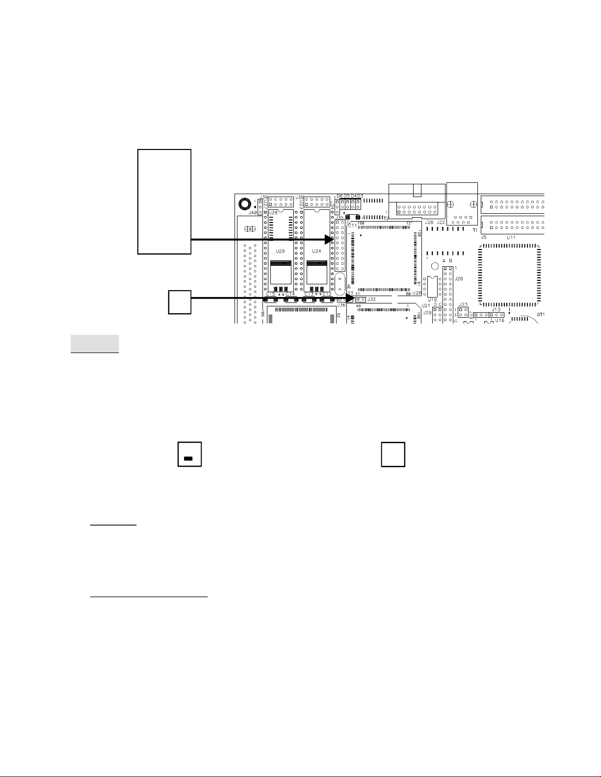
2.22 Eth er net Con figu ra tion
The Eth er net sec tion of the LBC- Plus uses the Na tional 83905 AT/LAN TIC Lo cal Area Net work
Twisted- Pair In ter face con trol ler. The AT/LAN TIC con trol ler is a CMOS/VLSI de vice used in the im ple men ta tion of CSMA/CD lo cal area net works. Sup ported net work in ter faces in clude 10BASE5 or
10BASE2 via an ex ter nal trans ceiver con nected to the AUI port, and twisted pair Eth er net (10B ASE-T)
us ing the on board trans ceiver. The AT/LAN TIC pro vides the Eth er net Me dia Ac cess Con trol ( MAC),
Encode- Decode (EN DEC) with an AUI in ter face, and 10BASE-T trans ceiver func tions in ac cor dan ce
with IEEE 802.3 stan dards.
This func tional block in cor po rates the re ceiver, trans mit ter, col li sion heart beat. loop b ack jab ber,
and link in teg rity blocks as de fined in the stan dard. The trans ceiver when com bined with the equali za tion re sis tors, trans mit/re ceive fil ters, and pulse trans form ers pro vide a com plete physi cal in ter face
from the AT/LAN TIC Con trol ler EN DEC mod ule and the twisted- pair me dium.
The in te grated EN DEC mod ule al lows the Man ches ter en cod ing and de cod ing via a dif fer en tial
trans ceiver and phase- lock- loop de coder at 10 Mbit/sec. Also in cluded are a col li sion de tec t trans la tor
and di ag nos tic loop back ca pa bil ity. The EN DEC mod ule in ter faces di rectly to the trans c eiver mod ule
and pro vides full IEEE com pli ant AUI (At tach ment Unit In ter face) for con nec tion to other m e dia trans ceiv ers.
The Me dia Ac cess Con trol (MAC) func tion is pro vided by the Net work In ter face Con trol (NIC)
mod ule which pro vides sim ple and ef fi cient packet trans mis sion and re cep tion con trol by m eans of off chip mem ory which can be ac cessed ei ther through an I/O port or mapped into the sys tem mem ory map.
An on board EPROM holds the Eth er net Ad dress and op tional con figu ra tion in for ma tion. This al lows for “jumper less” con figu ra tion us ing soft ware to con fig ure the board for its op er at ing mode, me dia type, I/O ad dress, in ter rupt, etc.
991206 OPERATIONS MANUAL LBC-Plus Page 2 - 29
WinSystems - "The Embedded Systems Authority"
J35
1 o o 2
3 o o 4
5 o o 6
7 o o 8
9 o o 10
11 o o 12
13 o o 14
15 o o 16
17 o o 18
19 o o 20
J32
1 2
o o
2.22.1 Jumpered vs. Jumper less Mode
The Eth er net sec tion can be con fig ured ei ther through the jumper block at J35 (de scribed lat er) or
via the con figu ra tion in for ma tion stored in the on board EE PROM. The source for the con figu ra tion in for ma tion is se lected via the jumper at J32 as shown here :
J32
1 2
o o
Jumpered Mode
Jumperless Mode
J32
1 2
o o
NOTE : The choice of “jumpered” or “jumper less” is to tally ex clu sive. This means that if
“jumper less” mode is se lected, all of the jump ers on J35 are ig nored and the con figu ra tion i n for ma tion
comes to tally from the EE PROM. Simi larly if “jumpered” mode is se lected the in for ma tion in t he EE PROM (ex cept for the Eth er net Ad dress) is ig nored.
IM POR TANT NOTE : In ter rupts must AL WAYS be jumpered manu ally via the jumper block at
J30 (Sec tion 1.6) which matches the “jumpered” or “jumper less” in ter rupt selection.
Page 2 - 30 OPERATIONS MANUAL LBC-Plus 991206

WinSystems - "The Embedded Systems Authority"
The fol low ing sec tions de tail the J35 jump er ing when the “jumpered” mode is se lected.
2.22.2 I/O Port Se lec tion
The NE2000 sec tion of the LBC-Plus uses 32 con secu tive I/O ad dresses in the CPU’s I/O space.
The base ad dress is se lected us ing three pins on the J35 con figu ra tion jumper. The choices av ail able
are:
240H
280H
2C0H
300H
320H
340H
360H
None
J35
.
.
11 o o 12
13 o o 14
15 o o 16
17 o o 18
19 o o 20
300H
J35
.
.
11 o o 12
13 o o 14
15 o o 16
17 o o 18
19 o o 20
2C0H 320H 340H 360H
J35
.
.
11 o o 12
13 o o 14
15 o o 16
17 o o 18
19 o o 20
NONE 240H 280H
J35
.
.
11 o o 12
13 o o 14
15 o o 16
17 o o 18
19 o o 20
J35
.
.
11 o o 12
13 o o 14
15 o o 16
17 o o 18
19 o o 20
J35
.
.
11 o o 12
13 o o 14
15 o o 16
17 o o 18
19 o o 20
J35
.
.
11 o o 12
13 o o 14
15 o o 16
17 o o 18
19 o o 20
J35
.
.
11 o o 12
13 o o 14
15 o o 16
17 o o 18
19 o o 20
The proper jump er ing for each of these choices is shown in the fol low ing il lus tra tions.
991206 OPERATIONS MANUAL LBC-Plus Page 2 - 31

WinSystems - "The Embedded Systems Authority"
2.22.3 In ter rupt Se lec tion
The NE2000 sec tion needs an in ter rupt line for sig nal ing vari ous con di tions to the soft war e driver.
There are 8 pos si ble choices as shown here :
IRQ 3
IRQ 4
IRQ 5
IRQ 9
IRQ 10
IRQ 11
IRQ 12
IRQ 15
The proper jump er ing for the three rele vant jumper po si tions cor re spond ing to the avail abl e in ter rupt choices are shown here :
J35
.
.
5 o o 6
7 o o 8
9 o o 10
11 o o 12
13 o o 14
.
.
IRQ3
J35
.
.
5 o o 6
7 o o 8
9 o o 10
11 o o 12
13 o o 14
.
.
IRQ10
J35
.
.
5 o o 6
7 o o 8
9 o o 10
11 o o 12
13 o o 14
.
.
IRQ4
J35
.
.
5 o o 6
7 o o 8
9 o o 10
11 o o 12
13 o o 14
.
.
IRQ11
J35
.
.
5 o o 6
7 o o 8
9 o o 10
11 o o 12
13 o o 14
.
.
IRQ5
J35
.
.
5 o o 6
7 o o 8
9 o o 10
11 o o 12
13 o o 14
.
.
IRQ12
J35
.
.
5 o o 6
7 o o 8
9 o o 10
11 o o 12
13 o o 14
.
.
IRQ9
J35
.
.
5 o o 6
7 o o 8
9 o o 10
11 o o 12
13 o o 14
.
.
IRQ15
Page 2 - 32 OPERATIONS MANUAL LBC-Plus 991206
WinSystems - "The Embedded Systems Authority"
2.22.4 I/O vs. Shared Mem ory Mode
The Eth er net buffer RAM can be ac cessed in ei ther of 2 ways. In the typi cal NE2000 com pati bl e
mode, the RAM is ac cessed through the NIC via I/O ports. An al ter nate ac cess scheme is avail ab le us ing the shared mem ory mode. In this mode it is soft ware com pati ble with the WD8013EBT from Stan dard Mi cro sys tems (for merly West ern Digi tal). In this mode a 32K win dow in the PC adapter sp ace is
used to ac cess packet mem ory. The ad dress of this win dow is con trolled by the driver. For NE20 00
com pati bil ity the I/O mode should be se lected. The jump er ing for each of the ac cess modes i s shown
be low :
J35
.
.
3 o o 4
5 o o 6
7 o o 8
.
.
I/O Mode
Shared Mem ory Mode
J35
.
.
3 o o 4
5 o o 6
7 o o 8
.
.
2.22.5 Me dia Type Se lec tion
The me dia type is also jumper se lecta ble via 2 pins on J35. The avail able choices are :
Twisted- pair 10BASE-T J22
Thin Eth er net Coax
AUI2 J28
Twisted- pair 10BASE-T Re duced Squelch
1
3
The J35 jump er ing for each of the op tions is shown be low.
J35
1 o o 2
3 o o 4
5 o o 6
.
10 BASE-T THIN ETHERNET
J35
1 o o 2
3 o o 4
5 o o 6
.
J35
1 o o 2
3 o o 4
5 o o 6
.
.
1
AUI Non- Spec 10 BASE-T
1 o o 2
3 o o 4
5 o o 6
.
.
J35
2
1
The thin Eth er net mode is not us able with the LBC- Plus. If thin Eth er net is re quired, it is nec es sary
to se lect the AUI mode and use an ex ter nal trans ceiver.
2
The AUI is con nected via J28. An adapter ca ble, WinSystems part number CBL- 147-1, is avail -
able which ter mi nates in a stan dard DB15 con nec tor.
3
The non- spec twisted- pair mode with re duced squelch lev els al lows the use of longer ca ble len gths
than speci fied in the twisted- pair speci fi ca tion, or the use of ca ble with higher losses.
991206 OPERATIONS MANUAL LBC-Plus Page 2 - 33

WinSystems - "The Embedded Systems Authority"
2.22.6 Com pati ble Vs. En hanced Mode
The NE2000 sec tion uses two 32K byte buffer RAMs on board. In com pati ble mode, only 8K of
each RAM (to tal of 16K) is ac ces si ble to the driver. When the En hanced mode is cho sen the ful l 32K is
avail able from each RAM. This en hanced mode is gen er ally sup ported by the sup plied AT/LAN TIC
driv ers but may not be us able with ge neric NE2000 soft ware or driv ers. When in doubt, choose t he
com pati ble mode. The J35 jump er ing for the com pati ble and en hanced modes are shown here :
J35
.
.
17 o o 18
19 o o 20
Com pati ble Mode
J35
.
.
17 o o 18
19 o o 20
En hanced Mode
2.22.7 Status LEDs
There are 4 LEDs in stalled on the LBC-Plus used to give a vis ual in di ca tion of Eth er net stat us. The
color, lo ca tion, and gen eral de scrip tion of each LED is given here :
D3 RED Col li sion
D4 GREEN Trans mit
D5 GREEN Re ceiver
D6 YEL LOW Link
2.22.8 Boot ROM Se lec tion
The LBC- Plus sup ports the use of the re mote boot fea ture avail able from NOVELL, QNX, and
some other op er at ing sys tems by al low ing pro vi sions for a user in stalled BIOS ex ten sion ROM into
U23. Only a 27C010 EPROM de vice is sup ported in this mode al though only 32K is avail able for th e
code. If the BIOS ex ten sion is sup plied in a smaller de vice it will have to be re pro grammed i nto a
27C010 de vice. In or der to use this BIOS ex ten sion, the board must be con fig ured for the DOC mode.
(See sec tion 2.19 for de tails). It is also pos si ble to se lect the ad dress where the BIOS ROM will ap pear
by con fig ur ing the SSD Socket Re lo ca tion op tion in the BIOS fea tures menu of CMOS Setup.
NOTE : The Eth er net BOOT ROM sup port and on board SSD sup port are mu tu ally ex clu sive, only
one or the other may be used. Con tact Win Sys tems for boards that sup port this fea ture.
Page 2 - 34 OPERATIONS MANUAL LBC-Plus 991206

WinSystems - "The Embedded Systems Authority"
2.22.9 PlusCfg Con figu ra tion Util ity
When “jumper less” mode is se lected (Sec tion 2.22.1), the con figu ra tion is made via soft ware which
is then saved to the on board EE PROM. PLUSCFG.EXE along with MES SAGE.MSG can be run from
the pro vided floppy or can be cop ied to a hard disk. From the DOS com mand line PLUSCFG.EXE is
exe cuted by typ ing :
pluscfg [En ter]
The con figu ra tion pro gram will load and dis play the ba sic menu and con figu ra tion screen. I f any
AT/LANTIC, or NE2000 adapt ers are rec og nized, they will be dis played in a win dow on the right side
of the screen as shown here :
WinSystems
Thick/Thin/TPI
August 20, 1993 11:34PM
CONFIGURATION
Configure New Adapter
Display/Change Adapter Configuration
Diagnostics
Quit and Return to DOS
******* Make Selection using arrow keys and <enter> *******
******* Scroll through options using <tab> *******
PLUSCFG V1.17
AT/LANTIC ADAPTERS
I/O Port Mode IRQ
0x320 I/O Port 10
0x360 I/O Port 5
AT/LANTIC
Configuration
Software
From the main menu choose the de sired func tion. Each of the main menu op tions will be dis cussed
in the fol low ing sec tions.
991206 OPERATIONS MANUAL LBC-Plus Page 2 - 35

WinSystems - "The Embedded Systems Authority"
2.22.10 Con fig ure New Adapter
This screen is used to con fig ure an in stalled adapter that is not pres ent in the win dow on the right
side of the screen. Typi cally this would be a board that had it's I/O port set to “None”.
Two choices are pro vided to con fig ure the new adapter.
The “Con fig ure New Adapter Auto mati cally” will search out an un con fig ured adapter, if pres e nt,
sur vey the sys tem, and make auto mat ic choices for I/O ad dress and in ter rupts for what it be lieves are
free for use. The sys tem will then dis play a se ries of con figu ra tion op tions to the user. Th ese in clude :
Adapter Ar chi tec ture - I/O Port or Shared Mem ory
Se lect Ca ble In ter face - Thin Eth er net or Thick Eth er net or 10BASE-T
The sec ond prompt will only be pres ent if there is no ac tive ca ble at tached or if the pro gram is un able to de ter mine the me dia type.
WinSystems
Thick/Thin/TPI
August 20, 1993 11:34PM
CONFIGURATION
CONFIGURE NEW ADAPTER
Configure New Adapter Automatically
Configure New Adapter Manually
Return to previous menu
******* Make Selection using arrow keys and <enter> *******
******* Scroll through options using <tab> *******
PLUSCFG V1.17
AT/LANTIC
Configuration
Software
AT/LANTIC ADAPTERS
I/O Port Mode IRQ
0x320 I/O Port 10
_____
Page 2 - 36 OPERATIONS MANUAL LBC-Plus 991206

WinSystems - "The Embedded Systems Authority"
The “Con fig ure New Adapter Manu ally” pres ents a screen simi lar to the one shown be low :
WinSystems
Thick/Thin/TPI
August 20, 1993 11:34PM
CONFIGURATION AT/LANTIC ADAPTERS
CONFIGURE NEW ADAPTER MANUALLY
Novell Configuration - None
I/O Base Address - 0x240
Interrupt assignment - IRQ3
Physical Media - TPI (10BaseT)
Adapter Architecture - I/O Port
Boot Prom - No Boot Prom
Advanced Configuration Options
Temporarily Change Configuration
Save Configuration
Return to previous menu
******* Make Selection using arrow keys and <enter> *******
******* Scroll through options using <tab> *******
PLUSCFG V1.17
AT/LANTIC
Configuration
Software
Use the up and down ar row keys and tab key to change the dis played con figu ra tion to what is de sired and then se lect “Save Con figu ra tion” to pro gram the EE PROM with the se lected choices.
NOTE : PLUSCFG will not al low se lec tion of I/O ports, in ter rupts, or mem ory ad dresses that it be lieves are be ing used by other hard ware in the sys tem. If PLUSCFG re fuses to al low a de sired se lec tion
for what you know are valid choices, it will be nec es sary to use the “jumpered” mode, de scribed ear lier,
for con figu ra tion.
2.22.11 Dis play/Change Adapter Con figu ra tion
This op tion of the main menu pres ents the same screen as shown for “Con fig ure New Adapter
Manu ally”. Use the up and down ar row keys and the Tab key to al ter the con figu ra tion as de si red and
then se lect “Save Con figu ra tion” to pro gram the EE PROM with the new in for ma tion.
NOTE : PLUSCFG will not al low se lec tion of I/O ports, in ter rupts, or mem ory ad dresses that it be lieves are be ing used by other hard ware in the sys tem. If PLUSCFG re fuses to al low a de sired se lec tion
for what you know are valid choices, it will be nec es sary to use the “jumpered” mode, de scribed ear lier,
for con figu ra tion.
991206 OPERATIONS MANUAL LBC-Plus Page 2 - 37

WinSystems - "The Embedded Systems Authority"
2.22.12 Di ag nos tics
This third choice from the main menu al lows the se lec tion from the di ag nos tics sub- menu as s hown
in this screen :
WinSystems
Thick/Thin/TPI
August 20, 1993 11:34PM
INITIALIZATION AND DIAGNOSTICS
Adapter Initialization & disagnostics
Advanced Network Diagnostics
Return to previous menu
******* Make Selection using arrow keys and <enter> *******
******* Scroll through options using <tab> *******
2.22.13
Adapter Ini tiali za tion and Di ag nos tics
CONFIGURATION
PLUSCFG V1.17
AT/LANTIC
Configuration
Software
AT/LANTIC ADAPTERS
I/O Port Mode IRQ
0x320 I/O Port 10
0x360 I/O Port 5
This choice ini tial izes the se lected adapter and con firms I/O ad dress, in ter rupt, me dia typ e, etc. The
adapter should be con nected to the net work ca ble at this time. A sam ple screen is shown on the foll owing page :
Page 2 - 38 OPERATIONS MANUAL LBC-Plus 991206

WinSystems - "The Embedded Systems Authority"
WinSystems
Thick/Thin/TPI
August 20, 1993 11:34PM
CONFIGURATION
INITIALIZATION AND DIAGNOSTICS
Network Interface Controller (080017086050)..............................................OK
Buffer Memory Check................................................................................ ...OK
Check cable connection (Cable Connected)................................................OK
Interrupt Assignment (5)........................................................................... ....OK
Boot Prom Check (No Boot Prom)...............................................................OK
Press <ESC> to return to previous menu.
******* Make Selection using arrow keys and <enter> *******
******* Scroll through options using <tab> *******
PLUSCFG V1.17
AT/LANTIC ADAPTERS
I/O Port Mode IRQ
INITIALIZATION AND DIAGNOSTICS
AT/LANTIC
Configuration
Software
NOTE : The Ini tiali za tion and Di ag nos tics must be run and must pass bef ore any of the Ad vanced
di ag nos tics can be exe cuted.
2.22.14 Ad vanced Net work Di ag nos tics
The Ad vanced Net work Di ag nos tics screen is shown here :
WinSystems
Thick/Thin/TPI
August 20, 1993 11:34PM
CONFIGURATION
INITIALIZATION AND DIAGNOSTICS
ADVANCED NETWORK DIAGNOSTICS
Set up as a master station..
Setup as a slave station.
Show packets on network.
Return to previous menu
******* Make Selection using arrow keys and <enter> *******
******* Scroll through options using <tab> *******
PLUSCFG V1.17
AT/LANTIC
Configuration
Software
AT/LANTIC ADAPTERS
I/O Port Mode IRQ
0x320 I/O Port 10
0x360 I/O Port 5
991206 OPERATIONS MANUAL LBC-Plus Page 2 - 39

WinSystems - "The Embedded Systems Authority"
Three choices are pro vided for Ad vanced Net work Di ag nos tics
2.22.15 Setup as a Mas ter Sta tion
This en ables the board un der test to be set up as the Mas ter. The mas ter will ini ti ate test i ng. The
Slave must be en abled prior to start ing the Mas ter.
The sys tem will then re quest a packet repe ti tion length and af ter en tered will be gin the tes t.
2.22.16 Setup as Slave Sta tion
This choice should be made for a known good board. It will echo back across the net work all pack e ts
ini ti ated by the Mas ter.
2.22.17 Show Packet on Net work
This op tion dis plays in HEX and AS CII pack ets as they are re ceived from the net work. A sam pl e
screen is shown here :
WinSystems
Thick/Thin/TPI
August 20, 1993 11:34PM
RECEIVED PACKET CONTENTS
Received Status : 01 Next Pointer : 54 Receiver Length : 1493
Destination 0040F698A3E6 Source : 0040F6988448
Length/Type : 05C3 Hex HW CRC : D703A649 SW CRC : NORMAL
0450 98 7D D0 40 03 00 00 00 01 00 00 00 00 00 01 04 ..}.@.............
0460 51 33 33 87 02 01 00 00 00 04 00 20 44 6F 63 2D Q33..........(Doc-
0470 06 00 F0 76 41 47 44 53 54 4D 00 00 00 40 E1 7A ..vAGDSTM...@.z
0480 74 BF 05 00 02 77 4D 44 54 47 53 00 04 00 0C 77 t....wMDTGS....w
0490 41 43 50 52 0E 00 14 77 41 43 44 49 4E 4F 50 52 ACPR...wACDINO
04A0 53 54 55 58 4F 47 0E 00 26 77 41 43 44 49 4E 4F STUXMG..&aACDINO
04B0 50 52 53 54 55 58 4D 47 0C 00 38 77 49 54 45 4D PRSTUXMG..8wITEM
04C0 20 4B 45 59 0C 00 54 77 56 41 4C 49 44 20 54 52 KEY :..Hw###,
04D0 23 23 23 59 0C 00 54 77 56 41 4C 49 44 20 54 53 ###Y...TwALID.TR
04E0 41 4E 53 3A 07 00 64 77 23 23 23 2C 23 23 23 52 ANS:..dw###,###R
Press <ESC> when finished examining receive packet
PLUSCFG V1.17
2.22.18 Quit and Re turn to DOS
This main menu op tion ex its PlusCfg and re turns you to the DOS prompt.
AT/LANTIC
Configuration
Software
Page 2 - 40 OPERATIONS MANUAL LBC-Plus 991206

WinSystems - "The Embedded Systems Authority"
2.23 Multi I/O Con nec tor
The I/O to the pri mary se rial chan nels, the printer port, and key board are all ter mi nated via the con nec tor at J3. An adapter ca ble, part number CBL- 162-1, is avail able from Win Sys tems to adapt to the
con ven tional I/O con nec tors. The pin defi ni tions for J3 are shown here :
J3
COM1 - DCD
COM1 - RXD
COM1 - TXD
COM1 - DTR
COM1 - GND
COM2 - DSR
COM2 - RTS
COM2 - CTS
COM2 - RI
LPT - STROBE
LPT - PD0
LPT - PD1
LPT - PD2
LPT - PD3
LPT - PD4
LPT - PD5
LPT - PD6
LPT - PD7
LPT - ACK
LPT - BUSY
LPT - PE
LPT - SLCT
KEYBD - GND
KEYBD - KDATA
KEYBD - +5V
1 o o 2
3 o o 4
5 o o 6
7 o o 8
9 o o 10
11 o o 12
13 o o 14
15 o o 16
17 o o 18
19 o o 20
21 o o 22
23 o o 24
25 o o 26
27 o o 28
29 o o 30
31 o o 32
33 o o 34
35 o o 36
37 o o 38
39 o o 40
41 o o 42
43 o o 44
45 o o 46
47 o o 48
49 o o 50
COM1 - DSR
COM1 - RTS
COM1 - CTS
COM1 - RI
COM2 - DCD
COM2 - RSX
COM2 - TXD
COM2 - DTR
COM2 - GND
LPT - AUTOFD
LPT - ERROR
LPT - INIT
LPT - SLCTIN
LPT - GND
LPT - GND
LPT - GND
LPT - GND
LPT - GND
LPT - GND
LPT - GND
LPT - GND
KEYBD - GND
KEYBD - GND
KEYBD - CLK
KEYBD - +5V
991206 OPERATIONS MANUAL LBC-Plus Page 2 - 41

WinSystems - "The Embedded Systems Authority"
2.23.1 Jumper/Con nec tor Sum mary
Con nec tor/ De scrip tion Page Ref er ence
Jumper
J1 Par al lel I/O VCC En able jumper 2-22
J2 COM3/COM4 I/O Con nec tor 2-7
J3 Multi-I/O Con nec tor 2-41
J4 Par al lel I/O ports 0-2 2-22
J5 Par al lel I/O ports 3-5 2-22
J6 Par al lel port mode se lect 2-13
J7 Power/Re set Con nec tor 2-18
J8 COM1 mode se lect jumper 2-7
J9 COM2 mode se lect jumper 2-7
J10 COM1 mode se lect jumper 2-7
J11 COM2 mode se lect jumper 2-7
J12 CPU Speed Se lect jumper 2-2
J13 Mas ter bat tery en able jumper 2-17
J14 PCI Bus Clock se lect jumper 2-3
J15 Par al lel I/O En able jumper 2-21
J16 SSD Ar ray size se lect jumper 2-19
J17 Floppy disk I/O con nec tor 2-14
J18 IDE I/O Con nec tor 2-16
J19 Watch dog timer con figu ra tion jumper 2-16
J20 VGA BIOS size se lect jumper 2-25
J21 ECP mode DMA se lect jumper 2-14
J22 10BASET I/O con nec tor N/A
J23 COM3/COM4 En able Dis able Se lect jumper 2-6
J24 ECP DMA se lect jumper 2-14
J25 SSD/DOC Mode se lect jumper 2-19
J26 PC/104-8 con nec tor 2-15
J27 Video out put con nec tor 2-26
J28 Eth er net AUI con nec tor N/A
J29 PC/104- 16 Con nec tor 2-15
J30 In ter rupt rout ing header 2-4
J31 PCI Bus clock se lect jumper 2-3
J32 NE2000 Mode se lect jumper 2-30
J33 FPA50 Panel adapter I/O con nec tor 2-26
J34 U23 VBAT se lect jumper 2-20
J35 NE2000 Con figu ra tion jumper 2-31
J36 CPU Clock mul ti plier se lect 2-3
J37 SMI In ter rupt N/A
J38 U23 De vice type se lect jumper 2-20
J39 U27 De vice type se lect jumper 2-20
J40 U27 VBAT Se lect Jumper 2-20
Page 2 - 42 OPERATIONS MANUAL LBC-Plus 991206

3 Award BIOS Con figu ra tion
3.1 Gen eral In for ma tion
The LBC- Plus comes equipped with a stan dard AWARD BIOS with Setup in ROM that al lows us ers to mod ify the ba sic sys tem con figu ra tion. This type of in for ma tion is stored in batter y- backed
CMOS RAM so that it re tains Setup in for ma tion when power is turned off.
3.2 En ter ing Setup
To en ter setup, power on the com puter and press the DEL key im me di ate ly af ter the mes sage “ Press
DEL to En ter Setup” ap pears on the lower left of the screen. If the mes sage dis ap pears bef ore you re spond and you still wish to en ter setup, re start the sys tem by turn ing it OFF and then ON or by press ing
the RE SET but ton, if so equipped, or by press ing the CTRL, ALT and DEL key si mul ta ne ously. A l ter nately, un der cer tain er ror con di tions of in cor rect setup the mes sage :
“Press F1 to con tinue or DEL to En ter Setup”
may ap pear. To En ter Setup at that time press the DEL key. To at tempt to con tinue, ig nor ing t he er ror con di tion, press the F1 key.
3.3 Setup Main Menu
The main menu screen is dis played on the fol low ing page. Each of the op tions will be dis cussed in
this sec tion. Use the ar row keys to high light the de sired se lec tion and press EN TER to en te r the sub menu or to exe cute the func tion se lected.
991206 OPERATIONS MANUAL LBC-Plus Page 3 - 1

WinSystems - "The Embedded Systems Authority"
ROM PCI/ISA BIOS (2A4KD000)
CMOS SETUP UTILITY
AWARD SOFTWARE, INC.
STANDARD CMOS SETUP PASSWORD SETTING
BIOS FEATURES SETUP IDE HDD AUTO DETECTION
CHIPSET FEATURES SETUP SAVE AND EXIT SETUP
LOAD BIOS DEFAULTS EXIT WITHOUT SAVING
LOAD SETUP DEFAULTS
Esc : Quit :Select Item
F10 : Save & Exit Setup (Shift) F2 : Change Color
Time, Date. Hard Disk, Type...
↑ ↓ → ←
3.4 Stan dard CMOS Setup
The items in the Stan dard CMOS Setup menu are di vided into sev eral cate go ries. Each cate gory
may in clude one or more setup items. Use the ar row keys to high light the item and then use the P gUp,
PgDn, +.-. keys to se lect the de sired value for the item.
Date
The date for mat is <day>,< date>,< month>, <year>
day = The day, from Sun to Sat, de ter mined by the BIOS and is dis play only
Date = the date, from 1 to 31 (or the maxi mum for the cur rent month)
month = the month, JAN through DEC
year = The year, from 1900 to 2099
Time
The time is hour,minute,sec ond. The time is cal cu lated on the 24- hour, military- time clock suc h
that 1:00PM is 13:00:00.
Page 3 - 2 OPERATIONS MANUAL LBC-Plus 991206

WinSystems - "The Embedded Systems Authority"
ROM PCI/ISA BIOS (2A4KD000)
STANDARD CMOS SETUP
AWARD SOFTWARE, INC.
Date (mm:dd:yy) : Wed, Sep 25 1996
Time (hh:mm:ss): 13 : 28 : 46
HARD DISKS TYPE SIZE CYLS HEAD PRECOMP LANDZ SECTOR MODE
Primary Master : Auto 0 0 0 0 0 0 AUTO
Primary Slave : Auto 0 0 0 0 0 0 AUTO
Drive A : 1.44M, 3.5 in
Drive B: None
Video : EGA/VGA
Halt On : No Errors
Base Memory : 640K
Extended Memory : 19456K
Other Memory : 384K
Total Memory:
ESC : Quit : Select Item PU/PD/+/- : Modify
F1 : Help (Shift) F2 : Change Color
↑ ↓ → ←
Drive C / Drive D type
This cate gory iden ti fies the type of hard disk C or hard disk D that has been in stalled in the sys tem.
There are 46 pre de fined types and a user de fin able type. Types 1-46 are shown in the fol low in g ta ble.
Type Size Cyl in ders Heads Sec tors Pre comp Land zone
1 10 306 4 17 128 305
2 20 615 4 17 300 615
3 30 615 6 17 300 614
4 62 940 8 17 512 940
5 46 940 6 17 512 940
6 20 615 4 17 None 615
7 30 462 8 17 256 511
8 30 733 5 17 None 733
9 112 900 15 17 None 901
10 20 820 3 17 None 820
11 35 855 5 17 None 855
12 49 855 7 17 None 855
13 20 306 8 17 128 319
991206 OPERATIONS MANUAL LBC-Plus Page 3 - 3

WinSystems - "The Embedded Systems Authority"
14 42 733 7 17 None 733
15 Re served
16 20 612 4 17 0 663
17 40 977 5 17 300 977
18 56 977 7 17 None 977
19 59 1024 7 17 512 1023
20 30 733 5 17 300 732
21 42 733 7 17 300 732
22 30 306 5 17 300 733
23 10 977 4 17 0 336
24 40 1024 5 17 None 976
25 76 1224 9 17 None 1023
26 71 1224 7 17 None 1223
27 111 1224 11 17 None 1223
28 152 1024 15 17 None 1223
29 68 1024 8 17 None 1023
30 93 918 11 17 None 1023
31 83 925 11 17 None 1023
32 69 1024 9 17 None 926
33 85 1024 10 17 None 1023
34 102 1024 12 17 None 1023
35 110 1024 13 17 None 1023
36 119 1024 14 17 None 1023
37 17 1024 2 17 None 1023
38 136 1024 16 17 None 1023
39 114 918 15 17 None 1023
40 40 820 6 17 None 820
41 42 1024 5 17 None 1023
42 65 1024 5 26 None 1023
43 40 809 6 17 None 852
44 61 809 6 26 None 852
45 100 776 8 33 None 775
46 203 684 16 38 None 685
Press PgUp or PgDn to se lect a num bered hard disk type, or type the number and press ENTER.
Most manu fac tur ers sup ply type in for ma tion with their drives that can be used to help iden t ify the
proper drive type. Mod ern IDE drives sel dom fall into the pre de fined types and are usu ally bes t han dled
with the “auto” or “user” types. The “auto” mode, reads the hard disk type in for ma tion from the drive at
Page 3 - 4 OPERATIONS MANUAL LBC-Plus 991206

WinSystems - "The Embedded Systems Authority"
boot time and uses it to ac cess the drive. The “user” mode al lows for ei ther man ual or auto mat ic en try,
via the setup op tion “IDE Auto De tect” of the drive pa rame ters.
If you de cide to cre ate the user type manu ally, you must sup ply the re quired pa rame ters as t o Cyl in der count, Head count, Pre comp Cyl in der, Land ing Zone Cyl in der, and number of sec tors per tr ack.
On Hard disks larger than 528MB, it will be nec es sary to choose the Logi cal Block Ad dress ing
mode (LBA) if you wish the drive to be ac ces si ble as a sin gle drive let ter.
If there is not hard disk in stalled, be sure to se lect “None”.
Drive A type/Drive B type
This cate gory iden ti fies the type of floppy drives at tached as Drive A: or Drive B:. The choice s are
as fol lows :
NONE 360K, 5.25 in.
1.2M, 5.25 in.
720K, 3.5 in
1.44M, 3.5 in.
Video
This cate gory speci fies the type of video adapter used for the pri mary sys tem moni tor that mat ches
your video dis play board and moni tor. The avail able choices are :
EGA/VGA
CGA40
CGA80
MONO
The LBC- Plus has built- in VGA sup port so EGA/VGA should be se lected.
Er ror Halt
This cate gory de ter mines whether the sys tem will halt if a non- fatal er ror is de tected dur i ng the
power up self test. The choices are :
No Er rors : The sys tem will not be stopped for any er ror that may be de tected.
All Er rors : When ever the BIOS de tects a non- fatal er ror, the sys tem will be stopped and a pr ompt
will ap pear.
All, but Key board : The sys tem will not stop for a key board er ror, it will stop for all other e r rors.
All, but disk ette : The sys tem will not stop for disk er rors. All oth ers will re sult in a prom pt.
991206 OPERATIONS MANUAL LBC-Plus Page 3 - 5

WinSystems - "The Embedded Systems Authority"
All but Disk/Key : All er rors ex cept disk ette or key board will re sult in a halt and a prompt.
Mem ory
This cate gory is dis play only and is de ter mined by the BIOS POST (Power On Self Test).
Base Mem ory
The POST rou tines in the BIOS will de ter mine the amount of base (con ven tional) mem ory in stal led
in the sys tem The value of the base mem ory is typi cally 640K for sys tems with a Mega byte of me m ory
or greater.
Ex tended Mem ory
The BIOS de ter mines how much ex tended mem ory is pres ent dur ing the POST. This is the amount
of mem ory lo cated above 1MB in the CPU's mem ory ad dress space.
Other Mem ory
This re fers to mem ory lo cated in the 640K to 1024K ad dress space. This is mem ory that can be u sed
for dif fer ent ap pli ca tions. DOS may use this area to load de vice driv ers and TSRs to keep a s much base
mem ory free as pos si ble for ap pli ca tion pro grams. The most com mon use of this area is for s hadow
RAM.
3.5 Bios Fea tures Setup
Vi rus Warn ing
This op tion when en abled, pro tects the boot sec tor and par ti tion ta ble of the hard disk agai nst un au thor ized writes through the BIOS. Any at tempt to al ter these ar eas will re sult in an er ror me s sage and a
prompt to author ize the ac tiv ity.
CPU In ter nal Cache
This op tion, when en abled, pro vides maxi mum per form ance by cach ing in struc tions and data u s ing
the on- chip cache of the 486 or 586 proc es sor.
Ex ter nal Cache
This op tion, when en abled, fur ther en hances per form ance by cach ing recently used in struc ti ons and
data into fast SRAM.
Page 3 - 6 OPERATIONS MANUAL LBC-Plus 991206

WinSystems - "The Embedded Systems Authority"
Quick Power ON Self Test
This op tion, when en abled, speeds up the POST dur ing power up. If it is en abled, the BIOS will
shorten and/or skip some items dur ing POST.
ROM PCI/ISA BIOS (2A4KD000)
BIOS FEATURES SETUP
AWARD SOFTWARE, INC.
Virus Warning : Disabled Video BIOS Shadow : En abled
CPU Internal Cache : Enabled C8000-CFFFF Shadow : Enabled
External Cache : Enabled D0000-D7FFF Shadow : Disab led
Quick Power On Self Test : Disabled D8000-DFFFF Shadow : Disabled
Boot Sequence : A,C SSD Socket Relocate : Disabled
Swap Floppy Drive : Disabled
Boot Up Floppy Seek : Enabled
Boot Up NumLock Status : On
Boot Up System Speed : High
Gate A20 Option : Fast
Typematic Rate Setting : Disabled
Typematic Rate (Chars/Sec) : 6
Typematic Delay (Msec) : 250
Security Option : Setup
ESC : Quit : Select Item
F1 : Help PU/PD/+/- : Modify
F5 : Old Value Shift F2 : Color
F6 : Load BIOS Defaults
↑ ↓ → ←
Boot Se quence
This op tion de ter mines the boot at tempt se quence for the fixed disk and floppy disk.
The choices are:
C,A The sys tem will at tempt Hard disk boot first
A,C The sys tem will at tempt Floppy disk boot first
Swap Floppy Drive
This op tion al lows for swap ping of the A: and B: floppy drives with out ac tu ally re lo cat ing the
drives on the ca ble.
Boot Up Floppy Seek
Dur ing POST, when this op tion is en abled, the BIOS will de ter mine if the floppy drive is 40 tr ack or
80 tracks, If dis abled, no seek test will be per formed and no er ror can be re ported.
991206 OPERATIONS MANUAL LBC-Plus Page 3 - 7

WinSystems - "The Embedded Systems Authority"
Boot Up Num lock Status
This al lows user se lec tion of the Num lock state at boot time.
Boot Up Sys tem Speed
This op tion al lows speci fi ca tion of the proc es sor speed at boot time. The op tions are :
HIGH
LOW
Gate A20 Op tion
This op tion al lows for the se lec tion of the source for the gate A20 sig nal. The choices are :
Nor mal - Sour ced from the key board con trol ler
Fast - Sour ced from the Chipset
Type matic Rate Set ting
This op tion en ables or dis ables the type matic rate pro gram ming at boot time. Type matic is th e auto repeat func tion for the key board.
Type matic Rate
When the type matic rate set ting is en abled the type matic re peat speed is set via this op tion. The sup ported rates are :
6 char ac ters per sec ond
8 char ac ters per sec ond
10 char ac ters per sec ond
12 char ac ters per sec ond
15 char ac ters per sec ond
20 char ac ters per sec ond
24 char ac ters per sec ond
30 char ac ters per sec ond
Page 3 - 8 OPERATIONS MANUAL LBC-Plus 991206

WinSystems - "The Embedded Systems Authority"
Type matic De lay
When type matic rate set ting is en abled, this op tion speci fies the time in mil li sec onds bef ore auto repeat be gins. The sup ported val ues are :
250 mS
500 mS
750 mS
1000 mS
Se cu rity Op tion
This op tion al lows you to limit ac cess to the sys tem and setup, or just to setup. The choices a re :
Sys tem - The sys tem will not boot and ac cess will be de nied if the cor rect pass word is not en tered
at the prompt.
Setup - The sys tem will boot, but ac cess to Setup will be de nied if the cor rect pass word is no t en tered
at the prompt.
NOTE : To dis able se cu rity, se lect “Pass word Set ting” at the Setup Main Menu and then you will
be asked to en ter a pass word. Do not type any thing, just hit EN TER. Once the se cu rity is dis abled, the
sys tem will boot and you can en ter Setup freely.
Shad ow ing Op tions
When shad ow ing for a par ticu lar ad dress range is en abled, it in structs the BIOS to copy the BIOS
lo cated in ROM into DRAM. This shad ow ing from an 8- bit EPROM into fast 32- bit DRAM re sults in a
Multi- magnitude in crease in per form ance. The main BIOS is shad owed auto mati cally but there a re
other ar eas that may be se lected for shad ow ing as shown here :
Video BIOS Shadow - C000- C7FFF EGA/VGA BIOS ROM
C8000- CFFFF
D0000- D7FFF
D8000- DFFFF
SSD Socket Re lo ca tion
The LBC- Plus sup ports an op tional BIOS ex ten sion ROM in U27. This fea ture was im ple mented
pri mar ily to sup port net work boot ROMs but can be used for other pur poses by knowl edge able users.
Only 128K X 8 de vices (27C010 type) are sup ported, al though only 32K of the de vice may be used
for code. The board is con fig ured for the DOC mode as docu mented in the SSD con figu ra tion sec tion of
this man ual. This setup op tion al lows for the BIOS ex ten sion to be lo cated at any of sev era l ad dresses as
shown here :
991206 OPERATIONS MANUAL LBC-Plus Page 3 - 9

WinSystems - "The Embedded Systems Authority"
Dis abled
C8000
CC000
D0000
D4000
D8000
DC000
E0000
Note : This mode of us age is mu tu ally ex clu sive of any on board sili con disk us age. Fur ther note t hat
'Di sabled' must be se lected when any SSD mode is de sired.
3.6 Chipset Fea tures Setup
The op tions in this sec tion con trol the chipset pro gram ming at boot time. In most cases, the d e fault
set tings should be used un less you have a clear un der stand ing of the sig nifi cance of the cha nge. It is pos si ble us ing these op tions to cre ate a sys tem that will ei ther not boot or is very un sta ble or un re li able. If
this should oc cur, there are two meth ods to re turn the sys tem to a sta ble con figu ra tion. If the sys tem
works well enough to get into Setup, sim ply choose the “Load BIOS De faults” op tion and then se l ect
“Save and Exit Setup” to re store fac tory de faults. If the sys tem will not run well enough to ru n Setup, it
will be nec es sary to re move the bat tery source tem po rar ily un til the CMOS mem ory de cays. Ref er to
Sec tion 2.X for de tails on re ini tial iz ing the CMOS RAM.
Each of the op tions for the Chipset Fea tures Menu will be briefly dis cussed in the sections that fol low.
Auto Con figu ra tion
This op tion, when en abled, in structs the BIOS to auto- select the proper AT Bus Clock, the DRAM
read tim ing, the DRAM write tim ing, the SRAM read tim ing, and the SRAM write tim ing base upon t he
cal cu lated CPU speed. The de fault is “En abled”.
Page 3 - 10 OPERATIONS MANUAL LBC-Plus 991206

WinSystems - "The Embedded Systems Authority"
ROM PCI/ISA BIOS (2A4KD000)
CHIPSET FEATURES SETUP
AWARD SOFTWARE, INC.
Auto Configuration : Enabled
AT-BUS Clock : CLK/4
DRAM Read Timing : Normal
DRAM Write Timing : Normal
SRAM Read Timing : 3-1-1-1
SRAM Write Timing : 0 Wait
ISA I/O Recovery : Disabled
Fast-Back-to-Back : Disabled
On-Chip Local Bus IDE : Enabled
IDE Buffer for DOS & Win : Enabled
IDE HDD Block Mode : Disabled
IDE Primary Master PIO : Auto
IDE Primary Slave PIO : Auto
ESC : Quit : Select Item
F1 : Help PU/PD/+/- : Modify
F5 : Old Value Shift) F2 : Color
F6 : Load BIOS Defaults
↑ ↓ → ←
AT- BUS Clock
This op tion is avail able when the “Auto Con figu ra tion” op tion is dis abled. This al lows se l ec tion of
the speed of the AT- BUS clock. This clock is any of 5 sub- multiples of the proc es sor os cil la tor or is
fixed at 7.19MHz. The choices avail able are:
7.19MHz
CLK/3
CLK/4
CLK/5
CLK/6
CLK/8
DRAM Read Tim ing
This op tion con trols the read tim ing to the DRAM ar ray. The avail able op tions are shown here :
slow
nor mal - de fault
fast
fast est
991206 OPERATIONS MANUAL LBC-Plus Page 3 - 11

WinSystems - "The Embedded Systems Authority"
DRAM Write Tim ing
This op tion con trols the write tim ing to the DRAM ar ray. The avail able op tions are shown here :
slow
nor mal - de fault
fast
fast est
SRAM Read Tim ing
This op tion al lows for se lec tion of the tim ing pat terns used to ac cess the Cache RAM. The av ail able
choices are :
2- 1- 1-1
3- 1- 1-1 De fault
3- 2- 2-2
4- 2- 2-2
SRAM Write Tim ing
This op tion con trols the number of wait- states to be in serted dur ing cache write op era tions. The
choices are :
0 Wait
1 Wait De fault
ISA I/O Re cov ery
The CPU and lo cal bus are much faster than the stan dard for the ISA bus. Se lect ing en abled for this
op tion al lows ad di tional time for I/O de vices to re spond to the sys tem. The de fault is dis abled.
Fast Back- To- Back
When en abled, con secu tive write cy cles tar geted to the same slave be come fast back- to- back on the
PCI bus. The de fault set ting is dis abled.
On Chip Lo cal Bus IDE
This op tion when en abled al lows us age of the on board PCI Bus IDE con trol ler. The de fault is en abled.
Page 3 - 12 OPERATIONS MANUAL LBC-Plus 991206

WinSystems - "The Embedded Systems Authority"
IDE Buffer for DOS & Win
Se lect En abled to in crease through put to and from IDE de vices by us ing the on- chip read- ahe ad and
post- write IDE buff ers. Note that the use of the buffer may cause some slow IDE de vices to ap pe ar even
slower. The de fault is En abled.
IDE HDD Block Mode
Block mode is also called block trans fer, mul ti ple com mand, or mul ti ple sec tor read/write. I f the
IDE hard drive sup ports block mode, se lect En abled for the auto mat ic de tec tion of the op ti mal number
of block read/writes per sec tor that the drive can sup port. The de fault is dis abled.
IDE Pri mary Mas ter PIO
There are 5 trans fer modes avail able for hard disk IDE trans fers rang ing from mode 0 to mode 4
with each suc ces sive mode pro vid ing an in creased level of per form ance. Se lect ing “Auto” wi ll al low
the BIOS to auto mati cally se lect the op ti mum trans fer mode for the mas ter hard disk. The de fault set ting is Auto.
IDE Pri mary Slave PIO
Like the pre vious item, this op tion al lows for the se lec tion of any one of 5 IDE trans fer mod es or an
Auto se lec tion which al lows the BIOS to auto- optimize the IDE trans fers to/from the slave hard disk.
The de fault set ting is Auto.
3.7 Load BIOS Defaults
This main- menu op tion will cause the CMOS RAM to be loaded with the de fault val ues as signed by
the fac tory. These are usu ally con sid ered safe val ues and do not neces sar ily rep re sent the high est per form ance val ues.
3.8 Load Setup Defaults
This op tion will cause the CMOS RAM to be loaded with de fault setup val ues as signed by the fac tory. These are usu ally val ues that were de ter mined to give a higher level of per form ance alo ng with re li able op era tion.
991206 OPERATIONS MANUAL LBC-Plus Page 3 - 13

WinSystems - "The Embedded Systems Authority"
3.9 Password Setting
This op tion al lows the set ting of the se cu rity pass word. Press ing en ter at the pass word pr ompt dis ables the se cu rity func tion com pletely.
3.10 IDE HDD Auto Detection
This func tion al lows mod ern IDE fixed disks to be used to their maxi mum po ten tial by in ter r o gat ing the driver as to its pre ferred con figu ra tion of tracks,heads, and sec tors; and auto mati c ally load ing
these pa rame ters into a “user de fined” hard disk type.
3.11 Save & Exit Setup
This func tion writes all changes to CMOS RAM and re starts the sys tem.
3.12 Exit without Saving
This op tion ex its setup with out sav ing any changes made and then re starts the sys tem.
Page 3 - 14 OPERATIONS MANUAL LBC-Plus 991206

4 LBC-PLUS Sili con Disk Ref er ence
4.1 In tro duc tion
Win Sys tems pro vides sili con disk sup port for the LBC-Plus us ing four dif fer ent me dia types de pend ing upon the needs of the ap pli ca tion.
1. The LBC-Plus pro vides sup port for a boota ble ROM DISK with a size of up to 1.44 Mega bytes. A
sim ple disk im ag ing tech nique al lows for the easy crea tion and main te nance of ROM DISKs. Si nce the
boota ble ROM DISK is an ex act im age of a boota ble floppy disk ette, all test ing and de bug gin g can be
ac com plished us ing a floppy drive. Once the ap pli ca tion is ready for ROM, it's a sim ple mat ter to use
the MKDISK util ity to cre ate the EPROM files nec es sary for the boota ble ROM DISK equiva lent o f the
func tion ing floppy disk ette.
2. In ap pli ca tions re quir ing oc ca sional pro gram or data up dates PEROM, (Flash) disks of up to 1
Mega byte may be used as the boot me dia. On board sup port is pro vided for the for mat ting, read ing, and
writ ing of the Floppy drive emu lat ing PEROMs.
3. For Ap pli ca tions need ing to log data, up date the ap pli ca tion, or for con ven ience dur i ng de vel op ment, bat tery backed SRAM may be used as the boot me dia with a size of up to 1 Mega byte.
4. The LBC- Plus sup ports the M- Systems Disk- On- Chip De vices (DOC). These are sin gle chip de vices con tain ing the BIOS Ex ten sion, TFFS Flash File Sys tem, and a Flash ar ray rang ing in si ze from 1
Mega byte to 12 Mega bytes. These de vices emu late a hard disk at the BIOS level.
4.2 ROM DISK Us age
MKDISK is a menu-driven util ity for cre at ing the ROM im age(s) du pli cat ing the de sired flopp y
disk ette. MKDISK is in voked at the DOS com mand line with :
MKDISK
Se lect the USSD mode from menu number 1. The other menu op tions are used with other Win Sys -
tems' Sili con Disk sys tems and are NOT com pati ble with the LBC- Plus board.
991206 OPERATIONS MANUAL LBC-Plus Page 4 - 1

WinSystems - "The Embedded Systems Authority"
MKDISK - Solid State RomDisk Creation Utility V6.00
(C) 1988-1994, WinSystems Inc.
SELECT SSD TYPE
Paged Memory Mode (SSD-XT)
Extended Memory Mode (SSD-AT)
V53 Expanded Memory Mode
I/O Mapped Silicon Disk (USSD)
sx386 On Board ROMDISK
SBC53sx Expanded Memory Mode
SAT-V40 Expanded Memory Mode
Use arrow keys and ENTER to make your selection.
MKDISK - Main Menu
From menu number 2 se lect the ap pro pri ate source disk size and type.
MKDISK - Solid State RomDisk Creation Utility V6.00
(C) 1988-1994, WinSystems Inc.
SELECT SOURCE DISK TYPE
160 KB 5 1/4 Single Sided 8 Sectors 40 tracks
180 KB 5 1/4 Single Sided 9 Sectors 40 tracks
320 KB 5 1/4 Double Sided 8 Sectors 40 tracks
360 KB 5 1/4 Double Sided 9 Sectors 40 tracks
720 KB 3 1/2 Double Sided 9 Sectors 80 tracks
720 KB 5 1/4 Double Sided 9 Sectors 80 tracks
954 KB 3 1/2 Double Sided 9 Sectors 53 tracks
960 KB 5 1/4 Double Sided 15 Sectors 64 tracks
1.2 Meg 5 1/4 Double Sided 15 Sectors 80 tracks
1.4 Meg 3 1/2 Double Sided 18 Sectors 80 tracks
Use arrow keys and ENTER to make your selection.
MKDISK - Drive type Menu
Page 4 -2 OPERATIONS MANUAL LBC-Plus 991206

WinSystems - "The Embedded Systems Authority"
MKDISK - Solid State RomDisk Creation Utility V6.00
(C) 1988-1994, WinSystems Inc.
SELECT SOURCE DRIVE
Drive A
Drive B
Use arrow keys and ENTER to make your selection.
MKDISK - Drive Menu
Se lect the source drive as ap pro pri ate.
MKDISK - Solid State RomDisk Creation Utility V6.00
(C) 1988-1994, WinSystems Inc.
SELECT ROM SIZE
32K X 8 ROM (27C256 type)
64K X 8 ROM (27C512 type)
128K X 8 ROM (27C010 type)
256K X 8 ROM (27C020 type)
512K X 8 ROM (27C040 type)
1M X 8 ROM (27C080 type)
Use arrow keys and ENTER to make your selection.
MKDISK - ROM type Menu
From menu number 4, se lect the ap pro pri ate EPROM size for the ROM DISK. EPROM size
smaller than 512K are not us able with the LBC- Plus, but are pro vided as choices for use with oth er
Win Sys tems’ sili con disk de vices.
991206 OPERATIONS MANUAL LBC-Plus Page 4 - 3

WinSystems - "The Embedded Systems Authority"
MKDISK - Solid State RomDisk Creation Utility V6.00
(C) 1988-1994, WinSystems Inc.
SELECT OUTPUT FILE TYPE
Binary Image Files
Hex ROM Image Files
S-Record ROM image files
Use arrow keys and ENTER to make your selection.
MKDISK - Output Menu
From menu number 5, se lect the ap pro pri ate ROM im age file for mat that your EPROM pro gram mer ac cepts. Se lect ing the Bi nary ROM im age file for mat will re sult in the small est files. MKDISK will
then read the speci fied floppy disk ette and cre ate a ROMx.HEX or ROMx.S19 where x is the ROM
number in the se quence (start ing with 1) and the ex ten sion (.BIN, .HEX, .S19) in di cates the o ut put for mat for Bi nary, Hex, and Mo torola re spec tively. If more than one file is cre ated, it means tha t the disk
will span more than a sin gle EPROM. Once the ROM(s) have been cre ated us ing the im age files, in stall
the ROM(s), jumper for cor rect ROM size, and en able the Sili con Disk boot op tion. The next powe r up
should re sult in a boot from the A: Sili con Disk. The ac tual floppy drive, if pres ent, will the n be avail able as drive B:.
4.3 Bootable RAMDISK/FLASHDISK Usage
The LBC- Plus sup ports boota ble RAM DISKs and FLASH DISKs of up to 1 Mega byte in size.
512K X 8 Static RAMs/PEROMs can be in stalled in the board be gin ning at U27. One or two
RAMs/PEROMs can be in stalled and the de vice jump ers should be ap pro pri ately set as de scribed in
sec tion 2.20. Af ter powe rup, it is nec es sary to con fig ure the sili con disk for the ac tual size of the drive
us ing the SSDINIT util ity. SSDINIT is in voked at the DOS com mand line with :
SSDINIT [A: | B: ] disk_size[K | M]
the K or M ar gu ments are op tional and are ac tu ally ig nored. Val ues be low 32 are as sumed to be in
Mega bytes while val ues above 32 are as sumed to be in Ki lo bytes. An ex am ple might help to cla r ify. To
pre pare a 1Meg Flash or SRAM disk for for mat ting, type :
SSDINIT B: 1M
Page 4 - 4 OPERATIONS MANUAL LBC-Plus 991206

WinSystems - "The Embedded Systems Authority"
The disk is now pre pared for for mat ting. The sys tem must be re booted prior to for mat ting wi th the
sim ple DOS com mand :
for mat b: /s/u
Af ter the next re set the for mat ted sili con disk will boot as the A: drive. If it is ever nec e s sary to by pass the sili con disk boot in or der to re for mat or to boot the ac tual floppy drive, or the har d disk, sim ply
press the <CTRL><ALT><LSHIFT> keys si mul ta ne ously im me di ate ly fol low ing dis play of the B IOS
con figu ra tion BOX. The mes sage :
Sili con Disk Boot Aborted by User
will be dis played and the sys tem will boot from one of the avail able boot drives.
IM POR TANT NOTE : The FLASH DISK is fully write able at all times but is not rec om mended
for con tinu ous up dat ing or data log ging. The on board BIOS im ple ments a sim ple FAT based fi le sys tem (iden ti cal to a floppy disk) with no wear lev el ing im ple mented. The PEROMs can and will wear
out with ex ces sive write cy cles. AT MEL speci fies at least 10,000 write cy cles.
4.4 Non-Bootable RAMDISK Usage
A non boota ble RAM DISK is of ten de sired in con junc tion with a boota ble ROM DISK, FLASH DISK, or ro ta tional me dia. It can then be used for pro gram up dates, pa rame ter stor age, or d ata log ging
ap pli ca tions. a non- bootable RAM DISK uses the Win Sys tems Uni ver sal Solid State Disk Driver
(USSD) which is loaded via the boot me dia's CON FIG.SYS file with the en try :
de vice = ussd.sys /mod:p /pad:1ec /seg:e400 /psz:16 /inc:1 /spg:xx /dsz:yy
where the YYY in /DSZ:YYY is the size of the disk in Ki lo bytes and the XXX in the /SPG:XXX is
the start ing page ad dress in the ar ray for this sili con disk. This hexa deci mal value is ac tu ally the count of
16K byte blocks pre ced ing the start of the RAM DISK. The sim plest ap proach is to use the ta ble be low
to de ter mine the cor rect /SPG value.
To tal RAM/ROM/FLASH /SPG Value
Prior to this socket
None /SPG:80
512K /SPG:A0
1M /SPG:C0
991206 OPERATIONS MANUAL LBC-Plus Page 4 - 5

WinSystems - "The Embedded Systems Authority"
A cou ple of ex am ples might help to il lus trate. Sup pose we're boot ing from a floppy or hard d isk and
we have in stalled two 512K X 8 SRAMs. In or der to cre ate the de sired 1 Meg RAM DISK we would
need the line :
de vice = ussd.sys /mod:p /seg:e400 /psz:16 /inc:1 /pad:1ec /spg:80 /dsz:1024
which would in di cate that we wish to cre ate a disk of 1M (1024K) start ing at the be gin ning of the ar ray.
For an other ex am ple as sume that we want a 512K ROM DISK and a 512K RAM DISK. We would
cre ate our boota ble floppy with the CON FIG.SYS line :
de vice = ussd.sys /mod:p /pad:1ec /seg:e400 /psz:16 /inc:1 /spg:a0 /dsz:512
This would cre ate the 512K RAM DISK which will be pre ceded by the 512K of ROM DISK. We
would cre ate our ROM DISK as pre vi ously de scribed and place the EPROM into U27. We would in sta ll
our 512K SRAM into U23.
A fi nal ex am ple would be to use the non- bootable RAM DISK in U27 as a sec on dary sili con disk to
a DISK-ON-CHIP. In this case we are boot ing from the DISK- ON- CHIP and will in clude the fol low ing CON FIG.SYS com mand line :
de vice = ussd.sys /mod:p /seg:e000 /psz:16 /inc:1 /pad:1ec /spg:80 /dsz:512
this will cre ate a 512K RAM DISK in the sili con disk socket U27.
NOTE : USSD, as is the con ven tion with DOS instal la ble disk de vices, cre ates a drive with the
NEXT AVAIL ABLE drive let ter. Drives A: and B: are al ways re served for the physi cal floppy drive or
the BIOS sup ported boota ble Sili con Disk. In a sys tem with out a hard disk, the next avail able drive let ter would be C:. In a sys tem with one or more hard drive par ti tions, the sili con disk cre ated with USSD
will be the first avail able let ter fol low ing any other drive let ters al ready in use. Also not e that it is never
nec es sary to for mat a disk cre ated with USSD. The disks are self for mat ting us ing the size a nd ad dress
in for ma tion pro vided on the CON FIG.SYS in vo ca tion line. Dur ing ini tiali za tion, USSD ex am ines the
sili con disk to de ter mine if a disk al ready ex ists which matches the pa rame ters speci fied. If so, no ac tion
is taken and the disk is used as is. If there is not a disk of the type and size speci fied, it is cre ated.
Page 4 - 6 OPERATIONS MANUAL LBC-Plus 991206

WinSystems - "The Embedded Systems Authority"
4.5 Non-Bootable FLASHDISK Usage
The AT MEL 5 Volt Flash Parts (29C040/29C040A) may also be used as a non boota ble drive in a
man ner nearly iden ti cal to the RAM DISK us age de scribed in the pre vious sec tion. The only ch ange
when us ing USSD for the AT MEL PEROMs is the ad di tion of the /EPT:256 pa rame ter to the CON FIG.SYS line which in stalls the USSD driver. An ex am ple us ing a 512K EPROM for a ROM DISK and
a 512K PEROM de vice would need the line :
de vice = ussd.sys /mod:p /pad:1ec /seg:e400 /psz:16 /inc:1 /spg:a0 /dsz:512 /ept:256
in the CON FIG.SYS file on the floppy to be im aged. This in vo ca tion will cre ate a 512K Flash d isk
in the sec ond socket of the ar ray. Ref er to the pre vious sec tion on non- bootable RAM DISK us age for
ad di tional de tails re gard ing the USSD driver.
4.6 DiskOnChip Usage
The LBC- Plus sup ports the M- Systems DISK- ON- CHIP (DOC) flash de vice in sizes rang ing from
1MB to 12MB. The DOC de vice con tains a BIOS ex ten sion, the TFFS (Tiny Flash File Sys tem), and
the Flash mem ory all in a sin gle 32- pin de vice. The DOC, un like the other Win Sys tems’ SSD su p port
for the LBC- Plus, emu lates a hard disk rather than a floppy disk. The DOC can be used as a sec on dary
hard disk to a physi cal IDE drive or it can be the only hard disk in the sys tem.
The DOC is in stalled into the socket at U23. Ref er to the sec tion 2.19 for cor rect de vice jump er ing
and ena bling of the DOC.
4.6.1 DOC Initialization
The DOC is ini tial ized in an iden ti cal fash ion to a fixed disk. DOS is booted (from floppy or hard
disk), FDISK is run on the DOC drive (be sure to get the right drive), the sys tem is re booted and then the
DOC is for mat ted us ing the DOS for mat com mand.
If the /S switch was used dur ing for mat ting and there is no other fixed disk de vice speci fied or at tached to the sys tem the DOC will be come the boot de vice. If a hard disk is pres ent, the DOC wi ll be come a sec on dary fixed disk.
991206 OPERATIONS MANUAL LBC-Plus Page 4 - 7

5 WS16C48 Pro gram ming Ref er ence
5.1 In tro duc tion
This sec tion pro vides ba sic docu men ta tion for the in cluded I/O rou tines. It is in tended th at the ac com pa ny ing source code equip the pro gram mer with a ba sic li brary of I/O func tions for the W S16C48
or can serve as the ba sis from which ap pli ca tion spe cific code can be de rived.
5.2 Func tion Defi ni tions
This sec tion briefly de scribes each of the func tions con tained in the driver. Where nec es sary , short
ex am ples will be pro vided to il lus trate us age. Any ap pli ca tion mak ing use of any of the d river func tions
should in clude the header file “uio48.h”, which in cludes the func tion pro to types and the neede d con stant defi ni tions.
Note that all of the func tions util ize the con cept of “bit_number”. The “bit_number” is a value from
1 to 48 (1 to 24 for in ter rupt re lated func tions) that cor re lates to a spe cific I/O pin. Bi t_number 1 is port
0 bit 0 and con tin ues through to bit_number 48 at port 5 bit 7.
INIT_IO - Ini tial ize I/O, set all ports to in put
Syn tax
void init_io(un signed io_ad dress);
De scrip tion
This func tion takes a sin gle ar gu ment :
io_ad dress - The I/O ad dress of the WS16C48 chip.
There is no re turn value. This func tion ini tial izes all I/O pins for in put (Sets them high), d is ables all
in ter rupt set tings, and sets the im age val ues.
991206 OPERATIONS MANUAL LBC-Plus Page 5 - 1

WinSystems - "The Embedded Systems Authority"
READ_BIT - Reads an I/O port Bit
Syn tax
int read_bit(int bit_number);
De scrip tion
This func tion takes a sin gle ar gu ment :
bit_number - This is a value from 1 to 48 that in di cates the I/O pin to read from.
This func tion re turns the state of the I/O pin. A '1' is re turned if the I/O pin is low and a '0 ' is re turned
if the pin is high.
WRITE_BIT - Write a 1 or 0 to an I/O pin
Syn tax
void write_bit(int bit_number, int value);
De scrip tion
This func tion takes two ar gu ments
bit_number - This is value from 1 to 48, which is the bit to be acted upon.
Value - is ei ther 1 or 0.
This func tion al lows for writ ing of a sin gle bit to ei ther a '0' or a '1' as speci fied by the sec ond ar gu ment. There is no re turn value and other bits in the I/O port are not af fected.
Page 5 - 2 OPERATIONS MANUAL LBC-Plus 991206

WinSystems - "The Embedded Systems Authority"
SET_BIT - Set the speci fied I/O Bit
Syn tax
void set_bit(int bit_number);
De scrip tion
This func tion takes a sin gle ar gu ment :
bit_number - a value be tween 1 and 48 speci fy ing the port bit to be set.
This func tion sets the speci fied I/O port bit. Note that set ting a bit re sults in the I/O pin a c tu ally go ing low. There is no re turn value and other bits in the same I/O port are un af fected.
CLR_BIT - Clear the speci fied I/O Bit
Syn tax
void clr_bit(int bit_number);
De scrip tion
This func tion takes a sin gle ar gu ment :
bit_number - a value from 1 to 48 in di cates the bit number to clear.
This func tion clears the speci fied I/O bit. Note that clear ing the I/O bit re sults in the ac tu al I/O pin
go ing high. This func tion does not af fect any bits other than the one speci fied.
991206 OPERATIONS MANUAL LBC-Plus Page 5 - 3

WinSystems - "The Embedded Systems Authority"
ENAB_INT - En able Edge In ter rupt, Se lect Po lar ity
Syn tax
void enab_int(int bit_number, int po lar ity);
De scrip tion
This func tion re quires two ar gu ments :
bit_number - A value from 1 to 24 speci fy ing the ap pro pri ate bit
po lar ity - Speci fies ris ing or fal ling edge po lar ity de tect. The con stants RIS ING and FAL LING are de fined
in “uio48.h”
This func tion en ables the edge de tec tion cir cuitry for the speci fied bit at the speci fied po lar ity. It
does not un mask the in ter rupt con trol ler, in stall vec tors, or han dle in ter rupts when they oc cur. There is
no re turn value and only the speci fied bit is af fected.
DISAB_INT - Dis able Edge De tect In ter rupt De tec tion
Syn tax
void disab_int(int bit_number);
De scrip tion
This func tion re quires a sin gle ar gu ment :
bit_number - A value from 1 to 24 speci fy ing the ap pro pri ate bit.
This func tion shuts down the edge de tec tion in ter rupts for the speci fied bit. There is no re turn value
and no harm is done by call ing this func tion for a bit which did not have edge de tec tion in ter rupts en abled. There is no af fect on any other bits.
Page 5 - 4 OPERATIONS MANUAL LBC-Plus 991206

WinSystems - "The Embedded Systems Authority"
CLR_INT - Clear the speci fied pend ing in ter rupt
Syn tax
void clr_int(int bit_number);
De scrip tion
This func tion re quires a sin gle ar gu ment :
bit_number - The speci fied bit number from 1 to 24 to re set the in ter rupt.
This func tion clears a pend ing in ter rupt on the speci fied bit. It does this by dis abling and reena bling
the in ter rupt. The net re sult af ter the call is that the in ter rupt is no longer pend ing and is re armed for the
next tran si tion of the same po lar ity. Call ing this func tion on a bit that has not been en abl ed for in ter rupts
will re sult in its in ter rupt be ing en abled with an un de fined po lar ity. Call ing this func tion with no in ter rupt pend ing will have no ad verse af fect. Only the speci fied bit is af fected.
GET_INT - Re trieve bit number of pend ing in ter rupt
Syn tax
int get_int(void);
De scrip tion
This func tion re quires no ar gu ments and re turns ei ther a '0' for no bit in ter rupts pend ing or a value
be tween 1 and 24 rep re sent ing a bit number that has a pend ing edge de tect in ter rupt. The fu nc tion re turns with the first in ter rupt found and be gins its search at Port 0 Bit 0 pro ceed ing through to Port 2 Bit
7. It is nec es sary to use ei ther clr_int() or disab_int() to avoid re turn ing the same bit con tinu ously. This
func tion may ei ther be used in an ap pli ca tion's ISR or can be used in the fore ground to poll for bit tran si tions.
991206 OPERATIONS MANUAL LBC-Plus Page 5 - 5

WinSystems - "The Embedded Systems Authority"
5.3 Sam ple Pro grams
There are three sam ple pro grams in source code form in cluded on the LBC-Plus disk ette in the
UIO48 di rec tory. These pro grams are not use ful by them selves but are pro vided to il lus trate the us age
of the I/O func tions pro vided in UIO48.C.
FLASH.C
This pro gram was com piled with Bor land C/C++ ver sion 3.1 on the com mand line with :
bcc flash.c uio48.c
This pro gram il lus trates the most ba sic us age of the WS16C48. It uses three func tions from th e
driver code. The io_init() func tion is used to ini tial ize the I/O func tions and the set_bit() a nd clr_bit()
func tions are used to se quence through all 48 bits turn ing each on and then off in turn.
POLL.C
This pro gram was com piled with Bor land C/C++ ver sion 3.1 on the com mand line with :
bcc poll.c uio48.c
This pro gram il lus trates ad di tional fea tures of the WS16C48 and the I/O li brary func tions. It pro grams the first 24 bits for in put, arms them for fal ling edge de tec tion, and then polls us ing the li brary
rou tine get_int() to de ter mine if any tran si tions have taken place.
INT.C
This pro gram was com piled with Bor land C/C++ ver sion 3.1 on the com mand line with :
bcc int.c uio48.c
This pro gram is iden ti cal in func tion to the “poll.c” pro gram ex cept that in ter rupts are ac tive and all
up dat ing of the tran si tion coun ters is ac com plished in the back ground dur ing the in ter ru pt serv ice rou tine.
Sum mary
The source code for all three pro grams as well as the I/O rou tines are in cluded on the ac com pa ny ing
disk ette. The source code is also pro vided in printed form in AP PEN DIX F. These I/O rou tines a long
with the sam ple pro gram pro vided should pro vide for a good ba sis on which to build an ap pli c a tion us ing the fea tures of the WS16C48.
Page 5 - 6 OPERATIONS MANUAL LBC-Plus 991206

6 AP PEN DIX A - I/O Port Map
The fol low ing is a list of PC I/O ports. Ad dresses marked with a '-' are not used on the LBC- Pl us but
their use should be care fully quali fied so as not to con flict with other I/O boards. I/O ad dres ses marked
with a '+' are used on the LBC-Plus board and are unique to the Win Sys tems de sign. I/O Ad dresse s
marked with '**' are gen er ally un used and should be the ba sis for the first choices in I/O ad d ress se lec tion.
Hex Range Us age
000- 00F 8237 DMA #1
**010- 01F FREE
020- 021 8259 PIC #1
+022- 023 Fi nali 486 Chipset Reg is ters
**024- 03F FREE
040- 043 8254 Timer
**044- 05F FREE
060- 06F 8042 Key board Con trol ler
070- 071 CMOS RAM/RTC
**072- 07F FREE
080- 08F DMA Page Reg is ters
**090- 09F FREE
0A0- 0BF 8259 PIC #2
0C0- 0DF 8237 DMA #2
**0E0- 0EF FREE
0F0- 0F1 Co proc es sor Con trol
**0F2- 11F FREE
+120- 12F WS16C48 HDIO
**130- 1DF FREE
+1E0- 1EF SSD, Led, Watch dog con trol
1F0- 1FF Fixed Disk I/O
-200- 20F Joy stick port
-210- 21F PCM SSD I/O Ports
-220- 22F Sound blas ter I/O ports
**230- 237 FREE
-238- 23B BUS Mouse
**240- 277 FREE
278- 27F LPT1
**280- 2AF FREE
-2B0 -2DF EGA Video
-2E0 -2E7 GPIP In ter face
2E8- 2EF COM4
**2F0- 2F7 FREE
2F8- 2FF COM2
-300- 31F Pro to type Card
-320- 32F XT Hard Disk
**330- 377 FREE
-378- 37F Par al lel Printer
-380 -3AF SDLC
991206 OPERATIONS MANUAL LBC-Plus Page 6 - 1

WinSystems - "The Embedded Systems Authority"
-3B0 -3BB DMA
-3C0 -3CF EGA
3E8- 3EF COM3
3F0- 3F6 Floppy Disk
3F8- 3FF COM1
Page 6 - 2 OPERATIONS MANUAL LBC-Plus 991206

7 AP PEN DIX B - In ter rupt Map
No. Ad dress Type De scrip tion
0 00 CPU Di vide by 0
1 04 CPU Sin gle Step
386 De bug Ex cep tion
2 08 CPU NMI
3 0C CPU Break point
4 10 CPU Over flow
5 14 BIO Print Screen
186 Bound Ex cep tion
6 18 186 In va lid op code ex cep tion
7 1C 186 Co proc es sor un avail able
8 20 Hard ware IRQ0 - 18.2Hz heart beat
286 LIDT - Dou ble fault ex cep tion
9 24 Hard ware IRQ1 - Key board in ter rupt
286 Co proc es sor seg ment
A 28 Hard ware IRQ2 - XT Re served,
AT-Slaved Con trol ler
286 In va lid TSS ex cep tion
B 2C Hard ware IRQ3 - COM2
286 Seg ment not pres ent
C 30 Hard ware IRQ4 - COM1
286 Stack fault ex cep tion
D 34 Hard ware IRQ5 - XT Hard Disk, AT Free
286 Pro tec tion fault ex cep tion
E 38 Hard ware IRQ6 - Floppy Disk In ter rupt
386 Page fault ex cep tion
F 3C Hard ware IRQ7 - LPT1
10 40 BIOS Video BIOS func tions
286 Co proc es sor ex cep tion
11 44 BIOS BIOS Equip ment check
486 Align ment check ex cep tion
12 48 BIOS Mem ory Size func tion
13 4C BIOS BIOS Disk func tions
14 50 BIOS BIOS se rial func tions
15 54 BIOS Cas sette/pro tected mode
func tions
16 58 BIOS Key board BIOS func tions
17 5C BIOS BIOS printer func tions
18 60 BIOS SROM Ba sic En try point (IBM)
19 64 BIOS Boot loader func tion
1A 68 BIOS BIOS time of day func tions
1B 6C BIOS Key board break vec tor
1C 70 BIOS User chained timer tick
1D 74 BIOS Video Ini tiali za tion
1E 78 BIOS Floppy Disk pa rame ter ta ble
991206 OPERATIONS MANUAL LBC-Plus Page 7 - 1

WinSystems - "The Embedded Systems Authority"
1F 7C BIOS CGA graphic char ac ter font
20 80 MS- DOS Pro gram ter mi nate
21 84 MS- DOS DOS func tion call
22 88 MS- DOS Ter mi nate Ad dress
23 8C MS- DOS Ctrl- Break Ad dress
24 90 MS- DOS Fa tal Er ror Vec tor
25 94 MS- DOS Ab so lute disk read
26 98 MS- DOS Ab so lute disk write
27 9C MS- DOS Ter mi nate
28 A0 MS- DOS Idle Sig nal
29 A4 MS- DOS TTY out put
2A A8 MS- DOS MS- Net serv ices
2F BC MS- DOS Print Spool
30 C0 MS- DOS Long jump in ter face
33 CC MS- DOS Mouse func tions
3F FC MS- DOS Over lay in ter rupt
40 100 BIOS Floppy I/O when fixed disk
is pres ent
41 104 BIOS Fixed disk 1 pa rame ter ta ble
42 108 BIOS EGA Chain
43 10C BIOS EGA Pa rame ter ta ble pointer
44 110 BIOS EGA graph ics char ac ter font
4A 128 BIOS AT Alarm exit ad dress
50 140 BIOS AT Alarm in ter rupt
51 144 BIOS Mouse func tions
5A 168 NET Func tions
5B 16C NET Boot chain
5C 170 NET Net BIOS en try
67 19C MS- DOS EMS func tions
6D 1B4 VGA VGA Serv ice
70 1C0 Hard ware IRQ8 - Real Time clock
71 1C4 Hard ware IRQ9 - Re di rected IRQ2
72 1C8 Hard ware IRQ10 - Un as signed
73 1CC Hard ware IRQ11 - Un as signed
74 1D0 Hard ware IRQ12 - Un as signed
75 1D4 Hard ware IRQ13 - Un as signed
76 1D8 Hard ware IRQ14 - IDE Fixed Disk
77 1DC Hard ware IRQ15 - Un as signed
80 200
F0 3C0 Ba sic
F1 3C4
FF 3FC Not used
Page 7 - 2 OPERATIONS MANUAL LBC-Plus 991206
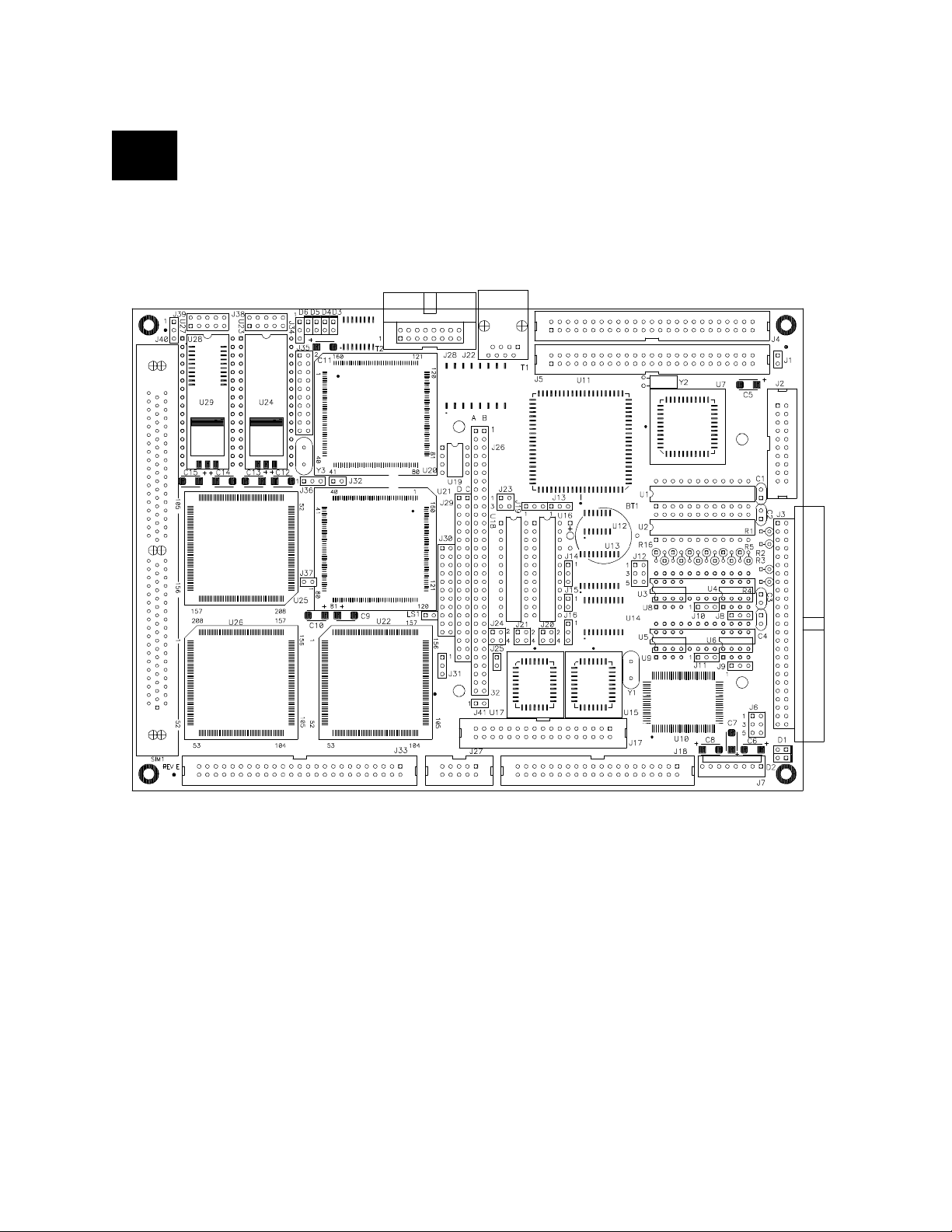
8 AP PEN DIX C
LBC-Plus Parts Place ment Guide - Top
991206 OPERATIONS MANUAL LBC-Plus Page 8 - 1
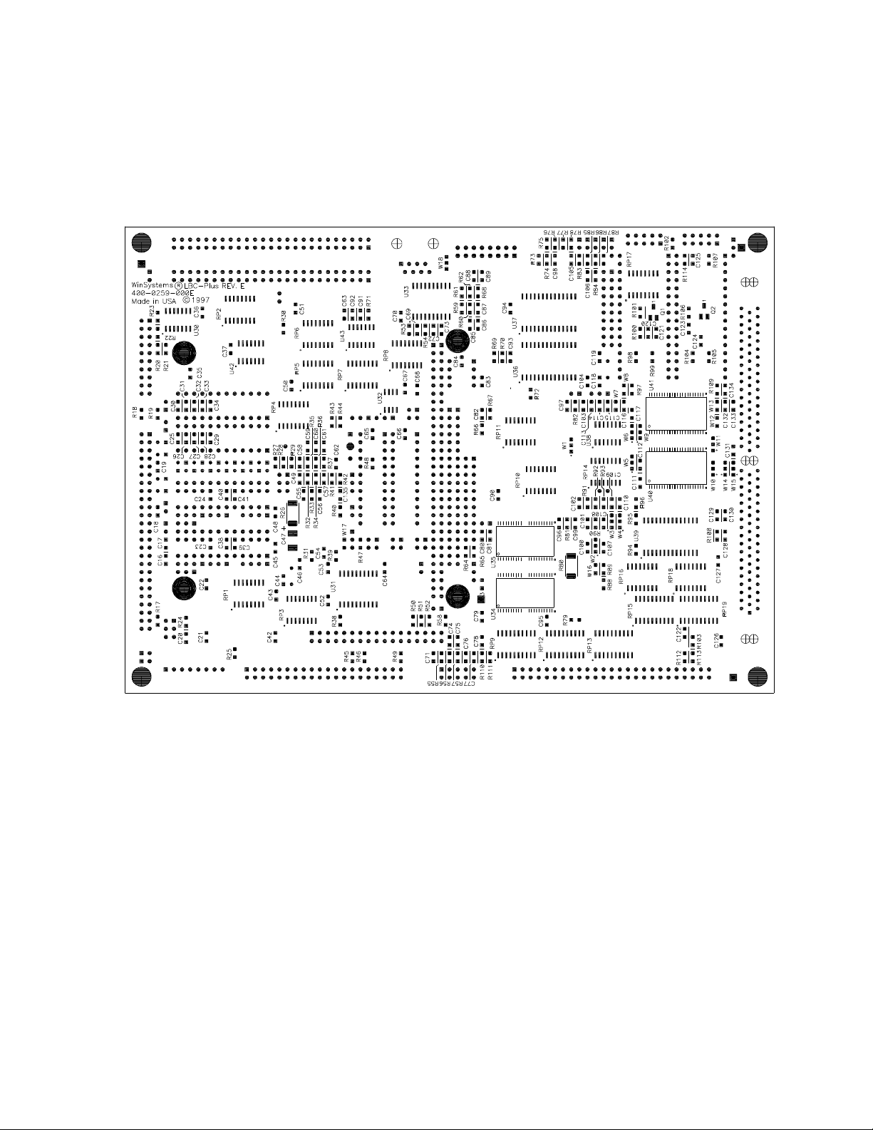
WinSystems - "The Embedded Systems Authority"
LBC- Plus Parts Place ment Guide -Bottom
Page 8 - 2 OPERATIONS MANUAL LBC-Plus 991206

9 APPENDIX D
LBC-PLUS Mechanical Drawing
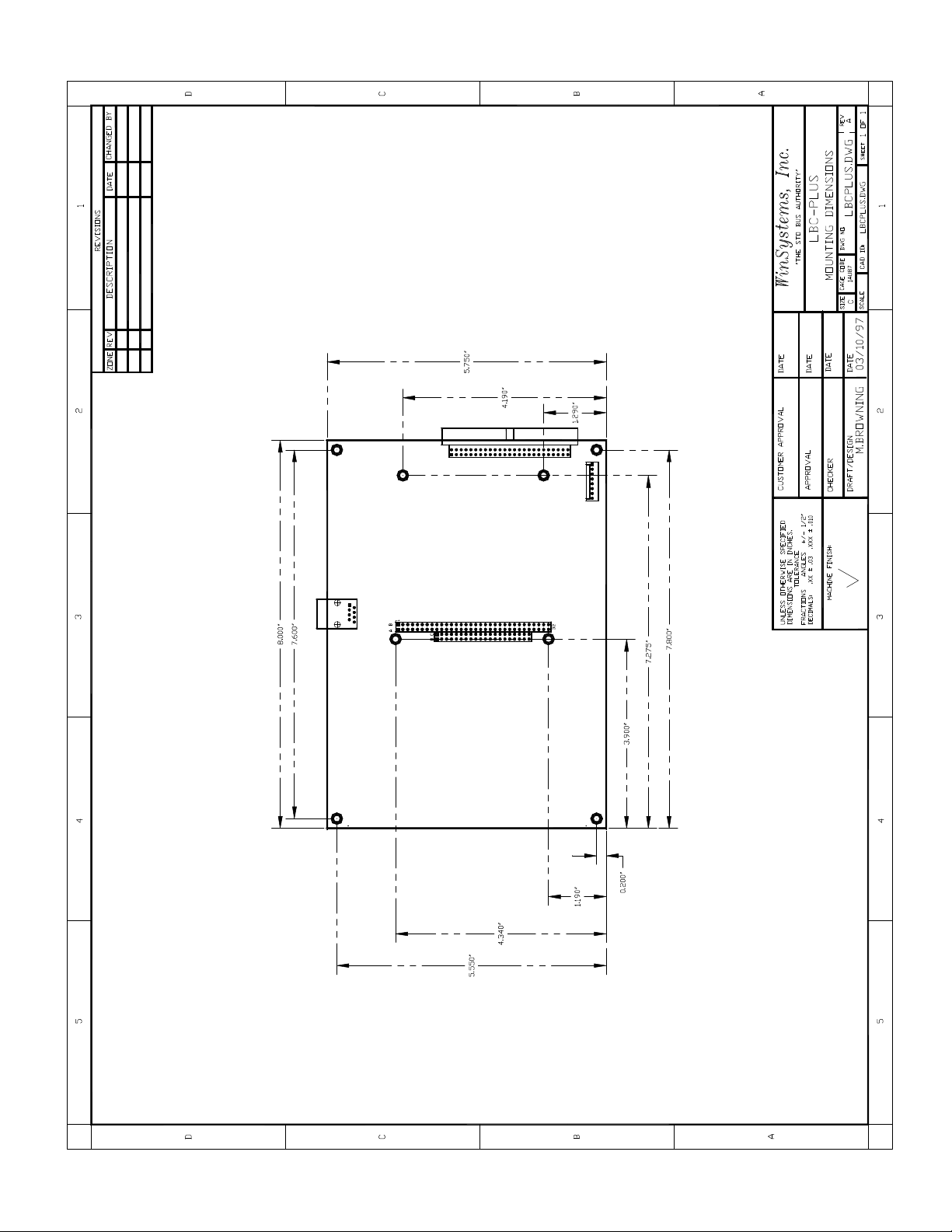

10 APPENDIX E
WS16C48 I/O Routines and Sample Program Listings

/* UIO48.H
Copyright 1996 by WinSystems Inc.
Permission is hereby granted to the purchaser of the WinSystems
UIO cards and CPU products incorporating the UIO device, to distribute
any binary file or files compiled using this source code directly or
in any work derived by the user from this file. In no case may the
source code, original or derived from this file, be distributed to any
third party except by explicit permission of WinSystems. This file is
distributed on an "As-is" basis and no warranty as to performance,
fitness of purposes, or any other warranty is expressed or implied.
In no case shall WinSystems be liable for any direct or indirect loss
or damage, real or consequential resulting from the usage of this
source code. It is the user's sole responsibility to determine
*/
/**************************************************************************
* Name : uio48.h
*
* Project : PCM-UIO48 Software Samples/Examples
*
* Date : October 30, 1996
*
* Revision: 1.00
*
* Author : Steve Mottin
*
****************************************************************************
*
* Changes :
*
* Date Revision Description
* ________ ________ ______________________________________________
* 10/30/96 1.00 Created
*
*****************************************************************************
*/
#define RISING 1
#define FALLING 0
void init_io(unsigned io_address);
int read_bit(int bit_number);
void write_bit(int bit_number);
void set_bit(int bit_number);
void clr_bit(int bit_number);
void enab_int(int bit_number, int polarity);
void disab_int(int bit_number);
void clr_int(int bit_number);
int get_int(void);
fitness for any considered purpose.

/* UIO48.C
Copyright 1996 by WinSystems Inc.
Permission is hereby granted to the purchaser of the WinSystems
UIO cards and CPU products incorporating the UIO device, to distribute
any binary file or files compiled using this source code directly or
in any work derived by the user from this file. In no case may the
source code, original or derived from this file, be distributed to any
third party except by explicit permission of WinSystems. This file is
distributed on an "As-is" basis and no warranty as to performance,
fitness of purposes, or any other warranty is expressed or implied.
In no case shall WinSystems be liable for any direct or indirect loss
or damage, real or consequential resulting from the usage of this
source code. It is the user's sole responsibility to determine
*/
/**************************************************************************
* Name : uio48.c
*
* Project : PCM-UIO48 Software Samples/Examples
*
* Date : October 30, 1996
*
* Revision: 1.00
*
* Author : Steve Mottin
*
****************************************************************************
*
* Changes :
*
* Date Revision Description
* ________ ________ ______________________________________________
* 10/30/96 1.00 Created
*
*****************************************************************************
*/
#include <dos.h>
/* This global holds the base address of the UIO chip */
unsigned base_port;
/* This global array holds the image values of the last write to each I/O
ports. This allows bit manipulation routines to work without having to
actually do a read-modify-write to the I/O port.
*/
unsigned port_images[6];
/*===========================================================================
* INIT_IO
*
* This function take a single argument :
*
*
* io_address : This is the base I/O address of the 16C48 UIO Chip
* on the board.
*
*
* This function initializes all I/O pins for input, disables all interrupt
* sensing, and sets the image values.
*
*===========================================================================*/
void init_io(unsigned io_address)
{
int x;
fitness for any considered purpose.
/* Save the specified address for later use */
base_port = io_address;
/* Clear all of the I/O ports. This also makes them inputs */
for(x=0; x < 7; x++)
/* Clear our image values as well */
for(x=0; x < 6; x++)
/* Set page 2 access, for interrupt enables */
outportb(base_port+7,0x80);
/* Clear all interrupt enables */
outportb(base_port+8,0);
outportb(base_port+9,0);
outportb(base_port+0x0a,0);
/* Restore normal page 0 register access */
outportb(base_port+7,0);
outportb(base_port+x, 0);
port_images[x] = 0;

}
port_images[bit_number / 8] = temp;
/*===========================================================================
*
* READ_BIT
*
*
* This function takes a single argument :
*
*
* bit_number : The integer argument specifies the bit number to read.
* Valid arguments are from 1 to 48.
*
* return value : The current state of the specified bit, 1 or 0.
*
* This function returns the state of the current I/O pin specified by
* the argument bit_number.
*
*===========================================================================*/
int read_bit(int bit_number)
{
unsigned port;
int val;
/* Adjust the bit_number to 0 to 47 numbering */
--bit_number;
/* Calculate the I/O port address based on the updated bit_number */
port = (bit_number / 8) + base_port;
/* Get the current contents of the port */
val = inportb(port);
/* Get just the bit we specified */
val = val & (1 << (bit_number % 8));
/* Adjust the return for a 0 or 1 value */
if(val)
}
/*===========================================================================
*
* WRITE_BIT
*
* This function takes two arguments :
*
*
* bit_number : The I/O pin to access is specified by bit_number 1 to 48.
*
* val : The setting for the specified bit, either 1 or 0.
*
* This function sets the specified I/O pin to either high or low as dictated
* by the val argument. A non zero value for val sets the bit.
*
*===========================================================================*/
void write_bit(int bit_number, int val)
{
unsigned port;
unsigned temp;
unsigned mask;
return 0;
return 1;
/* Adjust bit_number for 0 based numbering */
--bit_number;
/* Calculate the I/O address of the port based on the bit number */
port = (bit_number / 8) + base_port;
/* Use the image value to avoid having to read the port first. */
temp = port_images[bit_number / 8];/* Get current value */
/* Calculate a bit mask for the specified bit */
mask = (1 << (bit_number % 8));
/* Check whether the request was to set or clear and mask accordingly */
if(val) /* If the bit is to be set */
else
/* Update the image value with the value we're about to write */
temp = temp | mask;
temp = temp & ~mask;

/* Now actually update the port. Only the specified bit is affected */
/* Get the current state of the polarity register */
}
/*===========================================================================
* SET_BIT
*
*
* This function takes a single argument :
*
* bit_number : The bit number to set.
*
* This function sets the specified bit.
*
*===========================================================================*/
void set_bit(int bit_number)
{
}
/*===========================================================================
* CLR_BIT
*
*
* This function takes a single argument :
*
* bit_number : The bit number to clear.
*
* This function clears the specified bit.
*
*===========================================================================*/
void clr_bit(int bit_number)
{
}
/*===========================================================================
*
* ENAB_INT
*
* This function takes two arguments :
*
* bit_number : The bit number to enable intterups for. Range from 1 to 48.
*
* polarity : This specifies the polarity of the interrupt. A non-zero
* argument enables rising-edge interrupt. A zero argument
* enables the interrupt on the flling edge.
*
* This function enables within the 16C48 an interrupt for the specified bit
* at the specified polarity. This function does not setup the interrupt
* controller, nor does it supply an interrupr handler.
*
*============================================================================*/
void enab_int(int bit_number, int polarity)
{
unsigned port;
unsigned temp;
unsigned mask;
outportb(port,temp);
write_bit(bit_number,1);
write_bit(bit_number,0);
/* Adjust for 0 based numbering */
--bit_number;
/* Calculate the I/O address based uppon the bit number */
port = (bit_number / 8) + base_port + 8;
/* Calculate a bit mask based on the specified bit number */
mask = (1 << (bit_number % 8));
/* Turn on page 2 access */
outportb(base_port+7,0x80);
/* Get the current state of the interrupt enable register */
temp = inportb(port);
/* Set the enable bit for our bit number */
temp = temp | mask;
/* Now update the interrupt enable register */
outportb(port,temp);
/* Turn on access to page 1 for polarity control */
outportb(base_port+7,0x40);

temp = inportb(port); /* Get current polarity settings */
/* Set the polarity according to the argument in the image value */
if(polarity) /* If the bit is to be set */
else
/* Write out the new polarity value */
outportb(port,temp);
/* Set access back to Page 0 */
outportb(base_port+7,0x0);
}
/*===========================================================================
*
* DISAB_INT
*
* This function takes a single argument :
*
* bit_number : Specifies the bit number to act upon. Range is from 1 to 48.
*
* This function shuts off the interrupt enabled for the specified bit.
*
*===========================================================================*/
void disab_int(int bit_number)
{
unsigned port;
unsigned temp;
unsigned mask;
/* Adjust the bit_number for 0 based numbering */
--bit_number;
/* Calculate the I/O Address for the enable port */
port = (bit_number / 8) + base_port + 8;
/* Calculate the proper bit mask for this bit number */
mask = (1 << (bit_number % 8));
/* Turn on access to page 2 registers */
outportb(base_port+7,0x80);
/* Get the current state of the enable register */
temp = inportb(port);
/* Clear the enable bit int the image for our bit number */
temp = temp & ~mask;
/* Update the enable register with the new information */
outportb(port,temp);
/* Set access back to page 0 */
outportb(base_port+7,0x0);
}
/*==========================================================================
*
* CLR_INT
*
* This function takes a single argument :
*
* bit_number : This argument specifies the bit interrupt to clear. Range
* is 1 to 24.
*
*
* This function is use to clear a bit interrupt once it has been recognized.
* The interrupt left enabled.
*
*===========================================================================*/
void clr_int(int bit_number)
{
unsigned port;
unsigned temp;
unsigned mask;
temp = temp | mask;
temp = temp & ~mask;
/* Adjust for 0 based numbering */
--bit_number;

/* Calculate the correct I/O address for our enable register */
/* See if any bit set, if so return the bit number */
port = (bit_number / 8) + base_port + 8;
/* Calculate a bit mask for this bit number */
mask = (1 << (bit_number % 8));
/* Set access to page 2 for the enable register */
outportb(base_port+7,0x80);
/* Get current state of the enable register */
temp = inportb(port);
/* Temporarily clear only OUR enable. This clears the interrupt */
temp = temp & ~mask; /* clear the enable for this bit */
/* Write out the temporary value */
outportb(port,temp);
/* Re-enable our interrupt bit */
temp = temp | mask;
/* Write it out */
outportb(port,temp);
/* Set access back to page 0 */
outportb(base_port+7,0x0);
}
/*==========================================================================
*
* GET_INT
*
* This function take no arguments.
*
* return value : The value returned is the highest level bit interrupt
* currently pending. Range is 1 to 24.
*
* This function returns the highest level interrupt pending. If no interrupt
* is pending, a zero is returned. This function does NOT clear the interrupt.
*
*===========================================================================*/
int get_int(void)
{
int temp;
int x;
/* read the master interrupt pending register, mask off undefined bits */
temp = inportb(base_port+6) & 0x07;
/* If there are no interrupts pending, return a 0 */
if((temp & 7) == 0)
/* There is something pending, now we need to identify what it is */
/* Set access to page 3 for interrupt id registers */
outportb(base_port+7,0xc0);
/* Read interrupt ID register for port 0 */
temp = inportb(base_port+8);
return(0);
/* See if any bit set, if so return the bit number */
if(temp !=0)
{
}
/* None in Port 0, read port 1 interrupt ID register */
temp = inportb(base_port+9);
for(x=0; x <=7; x++)
{
}
if(temp & (1 << x))
{
}
outportb(base_port+7,0); /* Turn off access */
return(x+1); /* Return bitnumber with active int */

if(temp !=0)
{
}
/* Lastly, read status of port 2 int id */
temp = inportb(base_port+0x0a); /* Read port 2 status */
/* If any pending, return the appropriate bit number */
if(temp !=0)
{
}
/* We should never get here unless the hardware is misbehaving but just
to be sure. We'll turn the page access back to 0 and return a 0 for
no interrupt found.
*/
outportb(base_port+7,0);
}
return 0;
for(x=0; x <=7; x++)
{
}
for(x=0; x <=7; x++)
{
}
if(temp & (1 << x))
{
}
if(temp & (1 << x))
{
}
outportb(base_port+7,0); /* Turn off access */
return(x+9); /* Return bitnumber with active int */
outportb(base_port+7,0); /* Turn off access */
return(x+17); /* Return bitnumber with active int */

/* FLASH.C
Copyright 1996 by WinSystems Inc.
Permission is hereby granted to the purchaser of the WinSystems
UIO cards and CPU products incorporating the UIO device, to distribute
any binary file or files compiled using this source code directly or
in any work derived by the user from this file. In no case may the
source code, original or derived from this file, be distributed to any
third party except by explicit permission of WinSystems. This file is
distributed on an "As-is" basis and no warranty as to performance,
fitness of purposes, or any other warranty is expressed or implied.
In no case shall WinSystems be liable for any direct or indirect loss
or damage, real or consequential resulting from the usage of this
source code. It is the user's sole responsibility to determine
*/
#include <stdio.h>
#include <conio.h>
#include <dos.h>
#include "uio48.h"
/* This is where we have our board jumpered to */
#define BASE_PORT 0x200
/* This is an utlra-simple demonstration program of some of the functions
available in the UIO48 source code library. This program simply sets and
clears each I/O line in succession. It was tested by hooking LEDs to all
of the I/O lines and wathching the lit one race through the bits.
*/
void main()
{
int x;
fitness for any considered purpose.
/* Initialize all I/O bits, and set then for input */
init_io(BASE_PORT);
/* We'll repeat our sequencing until a key is pressed */
while(!kbhit())
{
}
}
getch();
/* We will light the LED attached to each of the 48 lines */
for(x=1; x <=48; x++)
{
}
/* Setting the bit lights the LED */
set_bit(x);
/* The wait time is subjective. We liked 100mS */
delay(100);
/* Now turn off the LED */
clr_bit(x);

/* POLL.C
Copyright 1996 by WinSystems Inc.
Permission is hereby granted to the purchaser of the WinSystems
UIO cards and CPU products incorporating the UIO device, to distribute
any binary file or files compiled using this source code directly or
in any work derived by the user from this file. In no case may the
source code, original or derived from this file, be distributed to any
third party except by explicit permission of WinSystems. This file is
distributed on an "As-is" basis and no warranty as to performance,
fitness of purposes, or any other warranty is expressed or implied.
In no case shall WinSystems be liable for any direct or indirect loss
or damage, real or consequential resulting from the usage of this
source code. It is the user's sole responsibility to determine
fitness for any considered purpose.
*/
#include <stdio.h>
#include <conio.h>
#include "uio48.h"
#define BASE_PORT 0x200
/* This program uses the edge detection interrupt capability of the
WS16C48 to count transitions on the first 24 lines. It does this
however, no by using true interrupts but by polling for transitions
using the get_int() function.
*/
/* Our transition totals are stored in this array */
unsigned int_counts[25];
/* Definitions for local functions */
void check_ints(void);
void main()
{
int x;
/* Initialize the I/O ports. Set all I/O pins to input */
init_io(BASE_PORT);
/* Initialize our transition counts, and enable falling edge
transition interrupts.
*/
for(x=1; x<25; x++)
{
}
/* Clean up the screen for our display. Nothing fancy */
clrscr();
for(x=1; x<25; x++)
{
}
/* We will continue to display until any key is pressed */
while(!kbhit())
{
}
}
void check_ints()
{
int current;
getch();
int_counts[x] = 0; /* Clear the counts */
enab_int(x,FALLING); /* Enable the falling edge interrupts */
gotoxy(1,x);
printf("Bit number %02d ",x);
/* Retrieve any pending transitions and update the counts */
check_ints();
/* Display the current count values */
for(x=1; x < 25; x++)
{
}
gotoxy(16,x);
printf("%05u",int_counts[x]);

/* Get the bit number of a pending transition interrupt */
current = get_int();
/* If it's 0 there are none pending */
if(current == 0)
/* Clear and rearm this one so we can get it again */
clr_int(current);
/* Tally a transition for this bit */
}
++int_counts[current];
return;

/* INTS.C
/* We will continuously print the transition totals until a
Copyright 1996 by WinSystems Inc.
Permission is hereby granted to the purchaser of the WinSystems
UIO cards and CPU products incorporating the UIO device, to distribute
any binary file or files compiled using this source code directly or
in any work derived by the user from this file. In no case may the
source code, original or derived from this file, be distributed to any
third party except by explicit permission of WinSystems. This file is
distributed on an "As-is" basis and no warranty as to performance,
fitness of purposes, or any other warranty is expressed or implied.
In no case shall WinSystems be liable for any direct or indirect loss
or damage, real or consequential resulting from the usage of this
source code. It is the user's sole responsibility to determine
fitness for any considered purpose.
*/
#include <stdio.h>
#include <dos.h>
#include <conio.h>
#include "uio48.h"
#define BASE_PORT 0x200
/* This program like the poll.c sample uses the edge detection interrupt
capability of the WS16C48 to count edge transitions. Unlike poll.c,
however this program actually uses interrupts and update all of the
transition counters in the background.
*/
/* Our transition totals are stored in this global array */
unsigned int_counts[25];
/* Function declarations for local functions */
void check_ints(void);
void interrupt int_handler(void);
void interrupt (*old_handler)(void);
void main()
{
int x;
/* Initialize the I/O ports. Set all I/O pins to input */
init_io(BASE_PORT);
/* Install an interrupt handler for the board */
/* We disable interrupts whenever we're changing the environment */
disable(); /* Disable interrupts during initialization */
/* Get the old handler and save it for later resoration */
old_handler = getvect(0x0d); /* Hardwired for IRQ5 */
/* Install out new interrupt handler */
setvect(0x0d,int_handler);
/* Clear the transition count values and enable the falling edge
interrupts.
*/
for(x=1; x<25; x++)
{
}
/* Unmask the interrupt controller */
outportb(0x21,(inportb(0x21) & 0xdf)); /* Unmask IRQ 5 */
/* Reenable interrupts */
enable();
/* Set up the display */
clrscr(); /* Clear the Text Screen */
for(x=1; x<25; x++)
{
}
int_counts[x] = 0; /* Clear the counts */
enab_int(x,FALLING); /* Enable the falling edge interrupts */
gotoxy(1,x);
printf("Bit Number %02d ",x);

*/
}
key is pressed */
/* All of the processing of the transition interrupts, including
updating the counts is done in the background when an interrupt
occurs.
*/
while(!kbhit())
{
}
getch();
/* Disable interrupts while we restore things */
disable();
/* Mask off the interrupt at the interrupt controller */
outportb(0x21,inportb(0x21) | 0x20); /* Mask IRQ 5 */
/* Restore the old handler */
setvect(0x0d,old_handler); /* Put back the old interrupt handler */
/* Reenable interrupts. Things are back they way they were before we
started.
enable();
for(x=1; x < 25; x++)
{
}
gotoxy(16,x);
printf("%05u",int_counts[x]);
/* This function is executed when an edge detection interrupt occurs */
void interrupt int_handler(void)
{
int current;
/* Get the current interrupt pending. There really should be one
*/
*/
}
here or we shouldn't even be executing this function.
current = get_int();
/* We will continue processing pending edge detect interrupts until
there are no more present. In which case current == 0
while(current)
{
/* Clear the current one so that it's ready for the next edge */
clr_int(current);
/* Tally up one for the current bit number */
++int_counts[current];
/* Get the next one, if any others pending */
}
/* Issue a non-specific end of interrupt command (EOI) to the
interrupt controller. This rearms it for the next shot.
*/
outportb(0x20,0x20); /* Do non-specific EOI */
current = get_int();

WARRANTY
WinSystems warrants that for a period of two (2) years from the date of shipment any Products and Software
purchased or licensed hereunder which have been developed or manufactured by WinSystems shall be free of any
material defects and shall perform substantially in accordance with WinSystems' specifications therefore. With
respect to any Products or Software purchased or licensed hereunder which have been developed or manufactured
by others, WinSystems shall transfer and assign to Customer any warranty of such manufacturer or developer held
by WinSystems, provided that the warrant y, if any, may be assigned. The sole obligation of WinSystems for any
breach of warranty contained herein shall be, at its option, either (i) to repair or replace at its expense any materially
defective Products or Software, or (ii) to take back such Products and Software and refund the Customer the
purchase price and any license fees paid for the same. Customer shall pay all freight, duty, broker's fees, insurance
changes and other fees and charges for the return of any Products or Software to WinSystems under this warranty.
WinSystems shall p ay freight and insurance charges for any repaired or replaced Products o r Software thereafter
delivered to Customer within the United States. All fees and costs for shipment outside of the United States shall be
paid by Customer. The foregoing warranty shall not apply to any Products or Software which have been subject to
abuse, misuse, vandalism, accidents, alteration, neglect, unauthorized repair or improper installations.
THERE ARE NO WAR RANTIES BY WINSYS TEMS EXCEPT AS STATED HEREIN. THERE ARE NO
OTHER WARRANTIES EXPRESS OR IM PLIED IN CLUD IN G, BUT NOT L IMITED TO, TH E IM PLIED
WARRANTIES OF MERCHANTABILITY AND FITNESS FOR A PARTICULAR PURPOSE, IN NO
EVENT SHALL WINSYSTEMS BE LIABLE FOR CONSEQUENTIAL, INCIDENTAL, OR SPECIAL
DAMAGES INCLUDING, BUT NOT LIMITED TO, DAMAGES FOR LOSS OF DATA, PROFITS OR
GOODWILL. WINSYSTEMS' MAXIMUM LIABILITY FOR ANY B REACH OF THIS AGREEM ENT OR
OTHER CLAIM RELATED TO ANY PRODUCTS, SOFTWARE, OR THE SUBJECT MATTER
HEREOF, SHALL NOT EXCEED THE PURCHASE PRICE OR LICENSE FEE PAID BY CUSTOMER
TO WINSYSTEMS FOR THE PRODUCTS OR SOFTWARE OR PORTION THEREOF TO WHICH
SUCH BREACH OR CLAIM PERTAINS.
WARRANTY SERVICE
All products returned to WinSyste ms must be assigned a Return Material Authorizatio n (RMA) number. To obtain
this number, please call or FAX WinS ystems' factory in Arlington, Texas and provide the following i nformation:
1. Description and quantity of the product(s) to be returned including its serial number.
2. Reason for the return.
3. Invoice number and date of purchase (if available), and original purchase order number.
4. Name, address, telephone and FAX number of the person making the request.
5. Do not debit WinSystems for the repair. W inSystems does not authorize debits.
After the RMA number is issued, please return the products promptly. Make sure the RMA number is visible on the
outside of the shipping package.
The customer must send the product freight prepaid and insured. The product must be enclosed in an anti-static bag
to protect it from damage caused by static electricity. Each bag must be completely sealed. Packing material must
separate each unit returned and placed as a cushion between the unit(s) and the sides and top of the shipping
container. WinSystems is not responsible for any damage to the product due to inadequate packaging or static
electricity.
 Loading...