

Page 1

OP ERA TIONS MAN UAL
EBC- BX
Win Sys tems re serves the right to make changes in the cir cuitry
Copy right 2003 by Win Sys tems. All Rights Re served.
and speci fi ca tions at any time with out no tice.
Page 2

RE VI SION HIS TORY
P/N 403- 0307- 000
ECO Num ber Date Code Rev Level
ORIGI NATED 030124 B
03- 57 030923 C
Page 3

TA BLE OF CON TENTS
Sec tion Para graph Page
Num ber Ti tle Num ber
1 Gen eral In for ma tion
1.1 Fea tures 1-1
1.2 Gen eral De scrip tion 1-1
1.3 Speci fi ca tions 1-2
2 EBC- BX Tech ni cal Ref er ence
2.1 In tro duc tion 2-1
2.2 In tel FW82430BX Chipset 2-1
2.3 Mem ory In stal la tion 2-1
2.4 In ter rupt Rout ing 2-2
2.5 Power/Re set Connections 2-3
2.6 Mouse In ter face 2-3
2.7 Real Time Clock/Calendar 2-4
2.8 Key board Interface 2-4
2.9 Se rial In ter face 2-5
2.10 Par al lel Printer Port 2-12
2.11 Speaker/Sound Interface 2-12
2.12 PC/104 In ter face 2-12
2.13 PC/104-Plus Bus Interface 2-13
2.14 Floppy Interface 2-14
2.15 IDE Hard Disk Interface 2-15
2.16 Watch dog Timer Con figu ra tion 2-16
2.17 Status LED 2-16
2.18 Bat tery Se lect Con trol 2-16
2.19 Disk OnChip Configuration 2-17
2.20 Par al lel I/O 2-18
2.21 VGA Configuration 2-21
2.22 Eth er net Con trol ler 2-23
2.23 Fan Power Con nec tor 2-24
2.24 Multi-I/O Con nec tor 2-25
2.25 USB Con nec tor 2-25
2.26 Jumper/Con nec tor Sum mary 2-26
3 Award BIOS Con figu ra tion
3.1 Gen eral In for ma tion 3-1
3.2 En ter ing Setup 3-1
3.3 Setup Main Menu 3-1
3.4 Stan dard CMOS Setup 3-2
3.5 Ad vanced BIOS Fea tures Setup 3-6
3.6 Chipset Fea tures Setup 3-11
3.7 In te grated Pe riph er als Setup 3-14
3.8 Power Man age ment Setup 3-19
3.9 PnP/PCI Configuration 3-23
Page 4

3.10 PC Health Status 3-25
3.11 Fre quency/Volt age Con trol 3-25
3.12 Load BIOS Defaults 3-26
3.13 Set Su per visor Pass word 3-27
3.14 Set User Password 3-27
3.15 Save & Exit Setup 3-27
3.16 Exit with out Sav ing 3-27
4 EBC- BX Disk On Chip Con figu ra tion
4.1 Disk On Chip Usage 4-1
4.2 DOC Ini tiali za tion 4-1
5 WS16C48 Pro gram ming Ref er ence
5.1 In tro duc tion 5-1
5.2 Func tion Defi ni tions 5-1
5.3 Sam ple Pro grams 5-6
AP PEN DIX A I/O Port Map
AP PEN DIX B In ter rupt Map
AP PEN DIX C EBC- BX Parts Place ment Guide
AP PEN DIX D EBC- BX Parts List
AP PEN DIX E EBC- BX Me chani cal Draw ing
AP PEN DIX F WS16C48 I/O Rou tines and Sam ple Pro gram List ings
Page 5

1 Gen eral In for ma tion
1.1 Fea tures
n In tel Low Power Cele ron Proc es sors and Low Power Pen tium III processors
n EBX- compliant board
n 256KB/128KB of pipe line burst L2 cache (Pen tium III/Cele ron)
n Up to 256MB of SDRAM
n Socket for boota ble Disk On Chip or DIP socket for BIOS ex ten sion sup port of Flash
or ROM
n PC Com pati ble uses In tel 443BX chip set
n On board high reso lu tion AGP 1X video controller
n Flat panel video support
n Sup ports reso lu tions up to 1280 x 1024
n Si mul ta ne ous CRT and LCD op era tion
n PC-104/Plus and PC/104 ex pan sion buses
n 10/100 Mbps Eth er net us ing In tel 82559
n 4 RS-232 se rial ports with FIFO, COM1 & COM2
supports op tional RS- 422/485/J1708 sup port
n Bi- directional LPT port sup ports EPP/ECP
n Dual IDE chan nels sup port UDMA -33 and UDMA- 66 Drives
n 48 bi- directional TTL digi tal I/O lines
1.2 Gen eral De scrip tion
The EBC-BX is a small, high- performance, em beddable com puter sys tem on a sin gle board. It in t e grates a number of popu lar I/O op tions in clud ing AGP 1X VGA, Eth er net, Solid- State Disk, and High Density Par al lel I/O. Four PC com pati ble se rial ports are stan dard, as are the floppy, hard disk, and par al lel printer in ter faces. The EBC-BX is popu lated with ei ther an In tel low power Celeron processor or
an Intel low power Pentium III processor at speeds from 300 to 700 MHz. Up to 256Mbytes of user
instal la ble DIMM mem ory is sup ported. A 16- bit PC/104 ex pan sion bus and the PC/104Plus bus is
pro vided for fur ther ex pan sion to an en tire in dus try of add- on pe riph er als in clud ing sound and speech
mod ules, SCSI con trol lers, Ana log I/O mod ules, and lit er ally hun dreds of other op tions avail able from
WinSystems and a va ri ety of ven dors sup port ing the PC/104 and PC/104-Plus stan dards. An on b oard
32-pin sili con disk socket sup port s the M-Systems’ Disk On Chip Flash mod ules in sizes rang ing from 8
Mega bytes to over 500 Mega bytes.
030923 OPERATIONS MANUAL EBC-BX Page 1 - 1
Page 6

1.3 Speci fi ca tions
1.3.1 Elec tri cal
Bus In ter face : PC/104 8- Bit or 16- Bit ex pan sion bus
PC/104-Plus 32- bit ex pan sion bus
Sys tem Clock : FSB 100MHz
In ter rupts : TTL Level in put
VCC : +5V +/- 5% at 2.75A typi cal with an In tel 400Mhz Celeron proc es sor with
32MB SDRAM
+5V +/-5% at 3.4A typi cal with an In tel Pen tium III proc es sor at 700 Mhz with
32MB SDRAM
VCC1 : +12V +/-5% (Not re quired. PC/104 Ex pan sion, Flat Panel, use only)
VCC2 : -12V +/-5% (Not required. PC/104 Ex pan sion or Flat Panel use only)
VCC3: 3.3V (Not re quired. PC/104 Plus ex pan sion use only)
Mem ory
Ad dress ing : 256 Mega byte ad dress ing
BIOS ROM : 256K Atmel Flash (re pro gram ma ble on board)
Mem ory DIMM Socket : 168-pin 3.3V Dimm Mod ule; PC-100 SDRAM Mod ule
SSD Mem ory : One 32- pin JE DEC stan dard socket sup port ing the M- Systems’ 32- Pin DOC
(Disk On Chip) mod ule.
1.3.2 Me chani cal
Di men sions : 5.75 X 8.0 X 0.60 inches (with out PC/104 mod ules or ca bles)
PC- Board : FR4 Ep oxy Glass with 6 sig nal lay ers and 4 power planes with screened
com po nent leg end, and plated through holes
Jump ers : 0.025" square posts on 0.10" cen ters
Con nec tors : Multi I/O : 50-pin RN type IDH- 50LP
COM3/COM4 : 20- pin RN type IDH- 20LP
Floppy Disk : 34-pin RN type IDH- 34- LP
Page 1 - 2 OPERATIONS MANUAL EBC-BX 030923
Page 7

CRT : 14-pin 2mm Mo lex Type 87331-1420
Flat Panel : Two, 50-pin 2mm Mo lex type 87331-5020
Power/Re set : 9-pin in- line Mo lex type 26- 60- 7091
Fan Power : 3-pin in- line Mo lex type 22- 11- 2032
Mouse : 5-pin in- line latch ing Mo lex type 22- 11- 2052
USB : 4-pin in- line latch ing Mo lex type 22-11-2042
PC/104 Bus : 64-Pin SAM TEC type ESQ- 132- 12- G-D
40-Pin SAM TEC type ESQ- 120- 12- G-D
PC/104- Plus Bus : 120-Pin SAM TEC type TS- 30-Q
IDE : Two 40-pin 2mm Mo lex Type 70246- 4021
Eth er net : RJ-45
1.3.3 En vi ron men tal :
Op er at ing Tem pera ture : -40° to +60° C
Non- condensing rela tive hu mid ity : 5% to 95%
030923 OPERATIONS MANUAL EBC-BX Page 1 - 3
Page 8

2 EBC- BX Tech ni cal Ref er ence
2.1 In tro duc tion
This sec tion of the man ual is in tended to pro vide suf fi cient in for ma tion re gard ing the con figu ra tion
and us age of the EBC- BX board. Win Sys tems main tains a Tech ni cal Sup port group to help an s wer
ques tions re gard ing con figu ra tion, us age, or pro gram ming of the board. For an swers to ques tions not
ade quately ad dressed in this man ual, con tact Tech ni cal Sup port at (817) 274- 7553 be tween 8AM and
5PM Cen tral Time.
2.2 In tel FW82443BX / SMSC Victory-66 Chipset
The EBC- BX util izes the In tel FW82443BX North bridge cou pled with the SMSC Victory- 66
South bridge. This com bined chipset pro vides a highly- integrated, high- performance back bone for full
Pen tium class com pati bil ity. The Chipset con tains the logic for DRAM and bus state con trol as well as
the stan dard com ple ment of 'AT' class pe riph er als, in clud ing :
Two-82C37 DMA con trol lers
Two-82C59 In ter rupt controllers
82C54 Timer/Counter
Real Time Clock
En hanced Power Man age ment
Full Plug and Play compatibility
These func tional units are 100% PC/AT com pati ble and are sup ported by the Award BIOS and
setup. Us ers de sir ing to ac cess these in ter nal pe riph er als di rectly should ref er to any manu fac tur ers ge neric lit era ture on the equiva lent dis crete com po nent.
There are a number of in ter nal reg is ters within the BX chipset that are used by the BIOS for con trol
and con figu ra tion. Ref er to the I/O map in Ap pen dix A for port us age to avoid con flicts when add ing ex ter nal I/O de vices.
2.3 Mem ory In stal la tion
The EBC- BX sup ports a sin gle user instal la ble 168- pin stan dard DIMM. DIMM mod ules should be
a mini mum speed of PC- 100 and x64 or x 72. Ei ther ECC on non- ECC parts may be used. A sin gle
DIMM socket is pro vided which can sup port SDRAM sizes from 32MB to 256MB. For a list of quali fied DIMMs, go to http://www.win sys tems.com/memory
In stal la tion is ac com plished with power off by in sert ing the DIMM mod ule di rectly into the con nec tor at M1. The DIMM mod ule is keyed in 2 places and can not be in serted back wards with out ex -
030923 OPERATIONS MANUAL EBC-BX Page 2 - 1
Page 9
WinSystems - "The Embedded Systems Authority"
treme force. The mod ule is in serted un til the re tain ing clips snap into place. Re moval is the re verse
pro cess. Push down on the re tain ing clips, mov ing them out ward. The DIMM mod ule, once re leased,
will be forced up to an ap pro pri ate re moval po si tion.
2.4 In ter rupt Rout ing
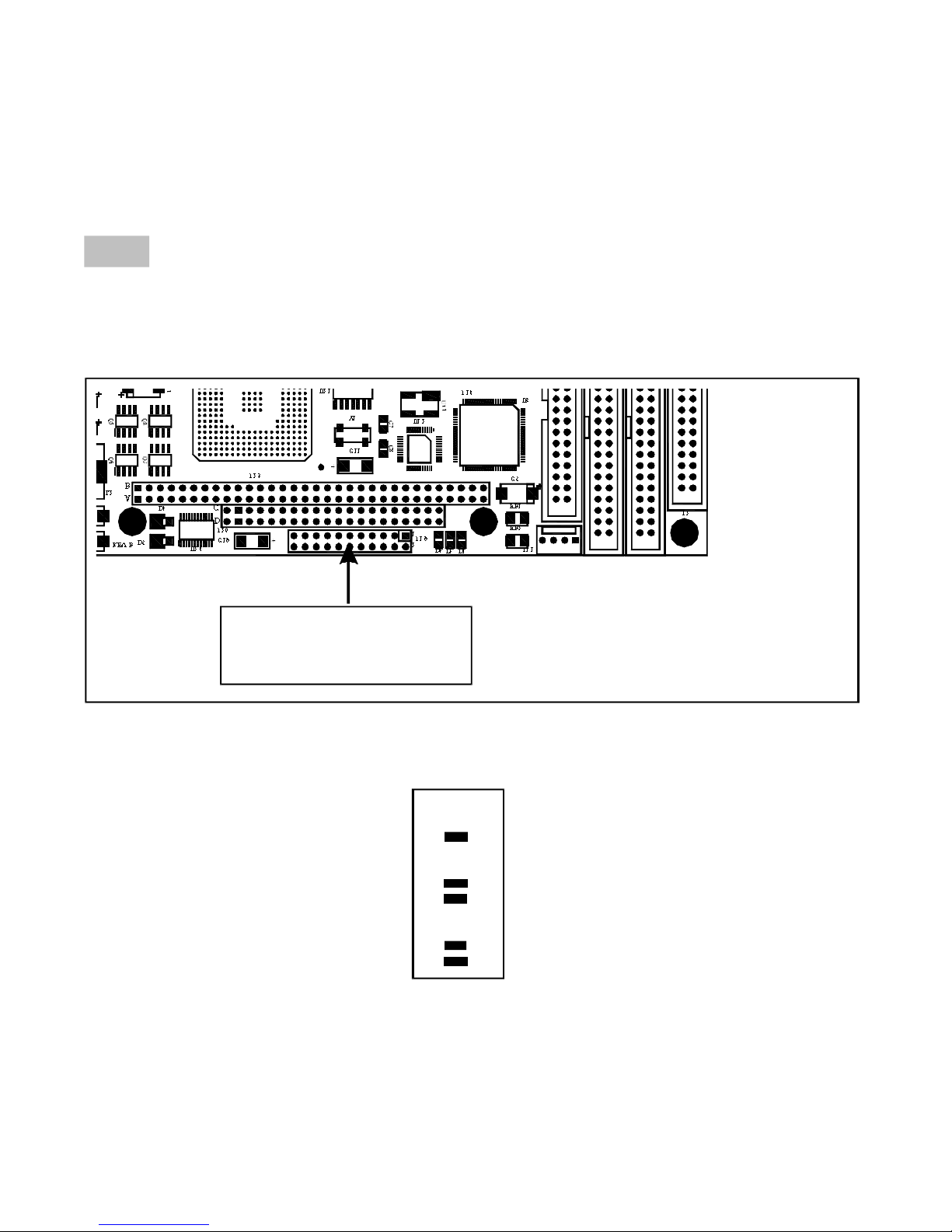
All in ter rupts on the EBC- BX are routed to their re spec tive PC/104 bus pins. On board non- PnP pe -
riph er als, are routed to their typi cal us age in ter rupts us ing the jumper block at J19. This block al lows
dis con nect ing or re rout ing of the on board in ter rupts. The lay out for the J19 header and the de fault
jumper set tings are shown be low.
21 19 17 15 13 11 9 7 5 3 1
o o o o o o o o o o o
o o o o o o o o o o o
22 20 18 16 14 12 10 8 6 4 2
J19
IRQ3
IRQ4
IRQ5
IRQ7
IRQ6
IRQ14
IRQ15
IRQ12
IRQ11
IRQ10
IRQ9
1 o o 2
3 o o 4
5 o o 6
7 o o 8
9 o o 10
11 o o 12
13 o o 14
15 o o 16
17 o o 18
19 o o 20
21 o o 22
In ter rupt rout ing header J19
N/C
N/C
COM3
N/C
N/C
Primary IDE
Secondary IDE
COM4
COM3
Parallel I/O
COM4
Page 2 - 2 OPERATIONS MANUAL EBC-BX 030923
Page 10

WinSystems - "The Embedded Systems Authority"
2.5 Power/Re set Con nec tions
Power is ap plied to the EBC- BX via the con nec tor at J3 (Mo lex part number 26-60-7091). The pin
defi ni tions for J3 are given be low. An op tional push- button- reset (Nor mally Open) may also be routed
into J3 if de sired. Mo men tary clo sure to ground forces a hard ware re set.
J3
o 1
+5V
+5V
o 2
o 3
o 4
o 5
o 6
o 7
o 8
o 9
GND
GND
+12V
+3.3V
GND
-12V
PB Reset
Note : The 3.3 Volt i nput pin does not pro vide power to any de vices on the board. It is routed di rectly to the PC/104Plus Bus and is only re quired if there are PC/104Plus cards that re quire 3.3 Volts be
sup plied from the Bus. The +12 and -12 Volt pins are routed di rectly to the PC/104 con nec tors and flatpanel con nec tors and are not re quired for nor mal board op era tion.
2.6 Mouse In ter face
A PS/2 mouse may be at tached via the con nec tor at J1. An adapter ca ble, CBL- 225-1 is avail able
from Win Sys tems to adapt to a con ven tional PS/2 mouse con nec tor. The pin out for J1 is shown here.
J1
MSDAT
GND
MSCLK
N/C
+5V
1 o
2 o
3 o
4 o
030923 OPERATIONS MANUAL EBC-BX Page 2 - 3
Page 11
WinSystems - "The Embedded Systems Authority"
2.7 Real Time Clock/Cal en dar
The EBC- BX con tains an on board Clock/Cal en dar within the Victory-66 chip. This clock is fully
com pati ble with the MC146818A used in the origi nal PC- AT com put ers. This clock has a number of
fea tures in clud ing pe ri odic and alarm in ter rupt ca pa bili ties. In ad di tion to the time and date keep ing
func tions, the sys tem con figu ra tion is kept within the CMOS RAM con tained in the clock sec tion. This
RAM holds all of the setup in for ma tion re gard ing hard and floppy disk types, video type, shad ow ing,
wait states, etc. Ref er to the sec tion on the Award BIOS Setup for what is con fig ured via the CMOS
RAM.
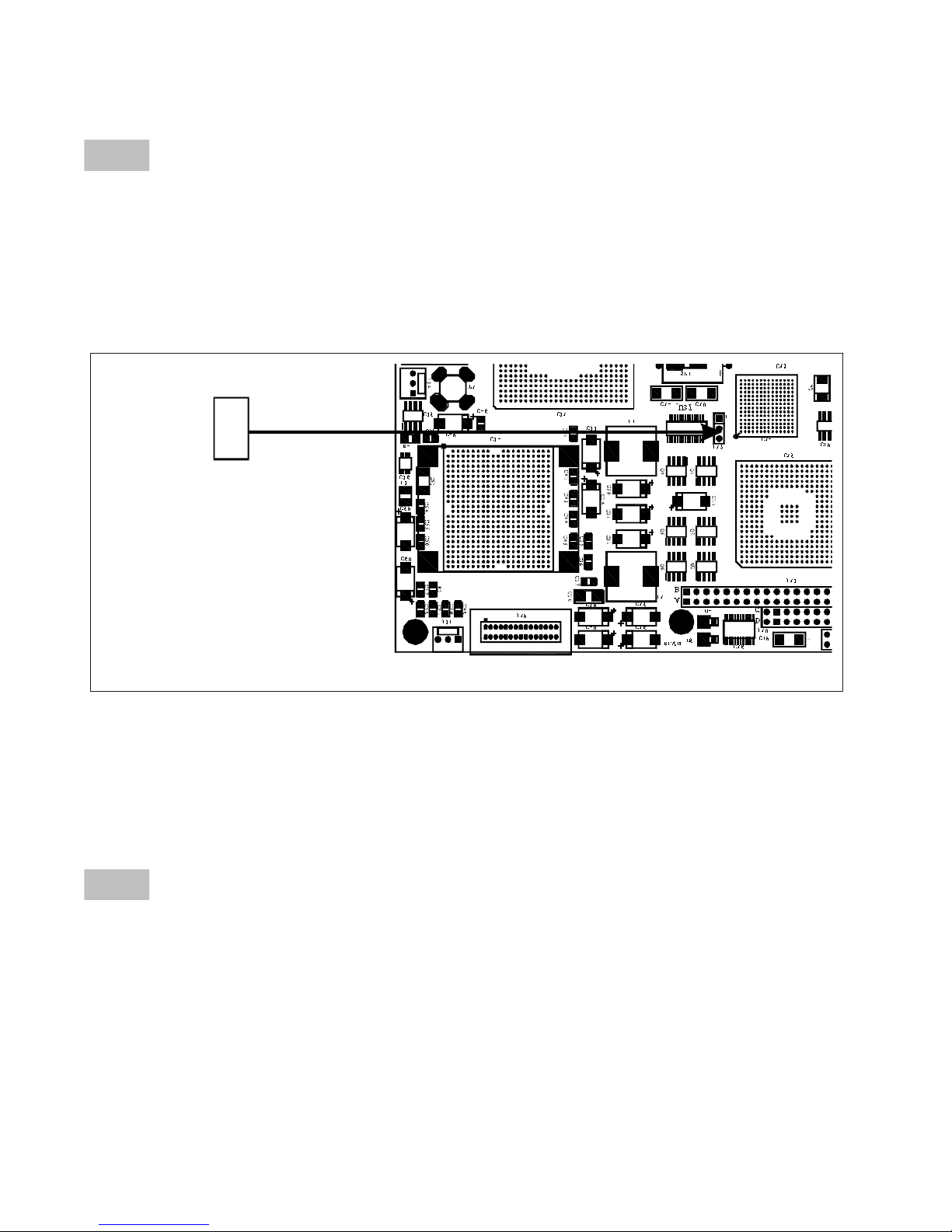
J27
1 o
2 o
3 o
J27 Bat tery Se lect Jumper
It may be come nec es sary at some time to make the CMOS RAM for get its cur rent con figu ra tion and
to start fresh with fac tory de faults. This may be ac com plished by re mov ing power from the board . Then
re move the jumper from pins 2-3 on J27 and place on pins 1-2 for 10 sec onds. Re place the jumper on
J27 pins 2-3, power- up, and re con fig ure the CMOS set tings as de sired.
If is de sired to op er ate the board with out a bat tery J27 must be jumpered on pins 1-2.
2.8 Key board In ter face
The EBC- BX con tains an on board PS/2 style key board con trol ler. Key board con nec tion is made
through the Multi-I/O con nec tor at J2. An adapter ca ble P/N CBL- 247-1 is avail able from Win Sys tems
to make ready ac cess to all of the de vices ter mi nated at the Multi-I/O con nec tor. Us ers de s ir ing cus tom
con nec tions should ref er to the Multi-I/O con nec tor pin defi ni tions given later in this man ual.
Page 2 - 4 OPERATIONS MANUAL EBC-BX 030923
Page 12
WinSystems - "The Embedded Systems Authority"
2.9 Se rial In ter face
1 o
2 o
3 o
J17
U10
1 o
2 o
3 o
J18
U4
3 2 1
o o o
J15
U6
3 2 1
o o o
J16
U5U9
U7
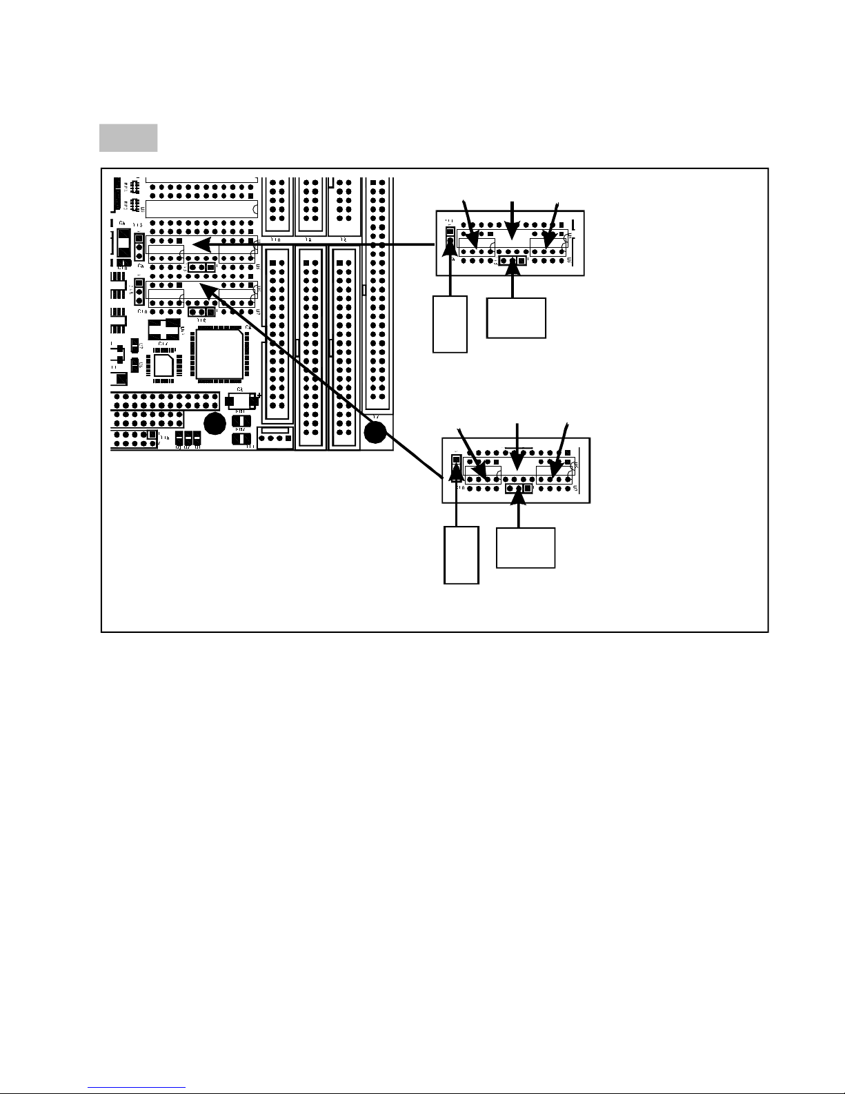
The EBC- BX pro vides four 16550 com pati ble RS- 232 se rial ports at the fol low ing ad dresses :
COM1 3F8H at IRQ 4 (PnP Device)
COM2 2F8H at IRQ 3 (PnP Device)
COM3 3E8H* at IRQ 5**
COM4 2E8H* at IRQ 9**
*COM ports 3 and 4 can be en abled or dis abled in di vidu ally via the jumper block at J24. When J24 pins
1-2 are jumpered, COM3 is en abled. When J24 pins 3-4 are jumpered, COM4 is en abled.
**The in ter rupts are not dis con nected when COM3 or COM4 are dis abled. Use the in ter rupt rout ing block
J19 de scribed ear lier to dis con nect the de fault in ter rupts if de sired.
030923 OPERATIONS MANUAL EBC-BX Page 2 - 5
Page 13

WinSystems - "The Embedded Systems Authority"
The two pri mary se rial ports, COM1 and COM2 are con fig ur able for RS- 422, RS- 485 or J1708,
with the ad di tion of op tional driver ICs (Win Sys tems P/N CK-75176-2). The con figu ra tion op tions for
each of the sup ported modes are shown on the fol low ing pages. Con nec tion to COM1 and COM2 is
made through the Multi-I/O con nec tor at J2. An adapter ca ble (P/N CBL- 247-1) is avail able from Win Sys tems to adapt to stan dard DB9 con nec tors.
COM1 - RS- 232
COM1 DB9
J15 J17
3 2 1
o o o
COM2 - RS- 232
J19 J22
3 2 1
o o o
1 2 3
o o o
1 2 3
o o o
U4 - In stalled
U9 - Not In stalled
U5 - Not In stalled
U6 - In stalled
U10 - Not In stalled
U7 - Not In stalled
CD
RX Data
TX Data
DTR
GND
CD
RX Data
TX Data
DTR
GND
1 o o 6
2 o o 7
3 o o 8
4 o o 9
5 o
COM2 DB9
1 o o 6
2 o o 7
3 o o 8
4 o o 9
5 o
DSR
RTS
CTS
RI
DSR
RTS
CTS
RI
Page 2 - 6 OPERATIONS MANUAL EBC-BX 030923
Page 14

WinSystems - "The Embedded Systems Authority"
COM3/COM4 - RS- 232
COM3 and COM4 are RS- 232 only and are ter mi nated at J4. An adapter ca ble is avail able from
WinSystems (P/N CBL-173-1), which adapts J4 to two stan dard DB9M con nec tors. The pin defi ni tions
for J4 are shown here :
J4
COM3 DCD
COM3 RX
COM3 TX
COM3 DTR
GND
COM4 DCD
COM4 RX
COM4 TX
COM4 DTR
GND
1 o o 2
3 o o 4
5 o o 6
7 o o 8
9 o o 10
11 o o 12
13 o o 14
15 o o 16
17 o o 18
19 o o 20
COM3 DSR
COM3 RTS
COM3 CTS
COM3 RI
N/C
COM4 DSR
COM4 RTS
COM4 CTS
COM4 RI
N/C
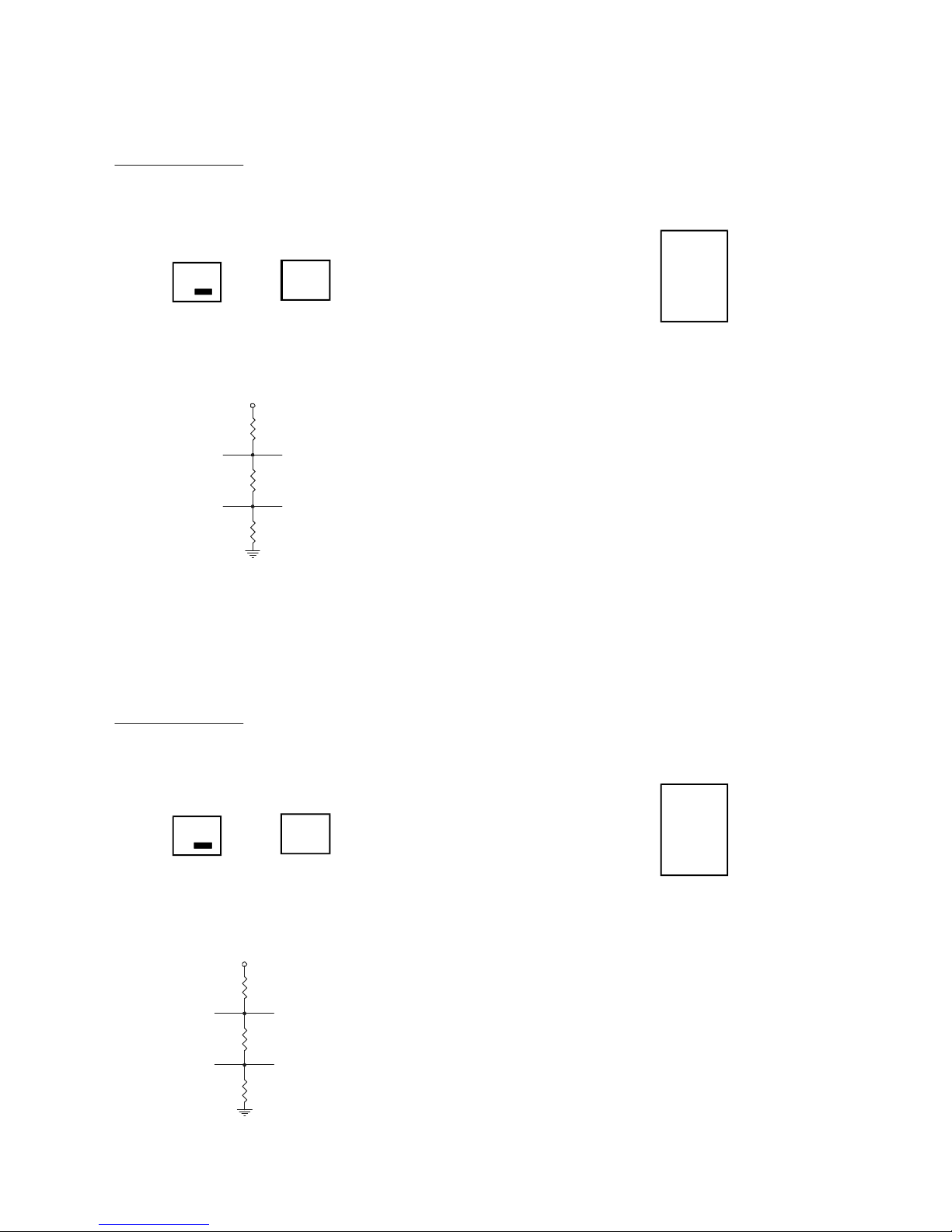
2.9.1 RS- 422 Mode Con figu ra tion
RS- 422 lev els are sup ported on both COM1 and COM2 with the in stal la tion of the op tional “Chip
Kit”, Win Sys tems part number CK- 75176-2. This kit pro vides the driver ICs nec es sary for a sin gle
chan nel of RS- 422. If two chan nels of RS- 422 are re quired then two kits will be needed. RS- 422 is a
4- wire point- to- point full- duplex in ter face al low ing much longer ca ble runs than are pos s i ble with RS-
232. The dif fer en tial trans mit ter and re ceiver twisted pairs of fer a high de gree of noise im mu nity. RS 422 usu ally re quires the lines be ter mi nated at both ends. This ter mi na tion can be ac com p lished ei ther
on the ca ble or by in stall ing re sist ers on the board in lo ca tions re served for them. The method for de ter min ing the cor rect re sis tor val ues is be yond the scope of this docu ment but it is rec om mended that trial
val ues of 100 ohms be used in all three lo ca tions at the re ceiver end. The fol low ing il lus t ra tion shows
the cor rect mode jump er ing, driver IC in stal la tion, I/O con nec tor pin defi ni tions, and ter mi na tion re sis tor lo ca tions for each of the chan nels when used in RS- 422 mode.
030923 OPERATIONS MANUAL EBC-BX Page 2 - 7
Page 15
COM1 - RS- 422
WinSystems - "The Embedded Systems Authority"
COM1 DB9
J15 J17
3 2 1
o o o
1 2 3
o o o
U4 - Not In stalled
U9 - In stalled
U5 - In stalled
N/C
TX+
TX-
N/C
GND
1 o o 6
2 o o 7
3 o o 8
4 o o 9
5 o
RX+
RXN/C
N/C
RS- 422 NOTE : When used in RS- 422 mode,
VCC
the trans mit ter must be en abled by set ting the RTS
bit in the Mo dem Con trol Reg is ter (Bit1).
R116
RX+
R114
RX-
R112
* Im por tant Note: All se rial ter mi na tion com po nents are sur face mount 0805 pack ages on the
bot tom side of the board. These should only be in stalled by sur face mount quali fied in di vidu als.
COM2 - RS- 422
J16 J18
3 2 1
o o o
VCC
R117
R115
R113
1 2 3
o o o
RX+
TX-
COM2 DB9
1 o o 6
U6 - Not In stalled
U10 - In stalled
U7 - In stalled
N/C
TX+
TX-
N/C
GND
2 o o 7
3 o o 8
4 o o 9
5 o
RS- 422 NOTE: When used in RS- 422 mode,
the trans mit ter must be en abled by set ting the RTS
bit in the Mo dem Con trol Reg is ter (Bit).
Page 2 - 8 OPERATIONS MANUAL EBC-BX 030923
Page 16
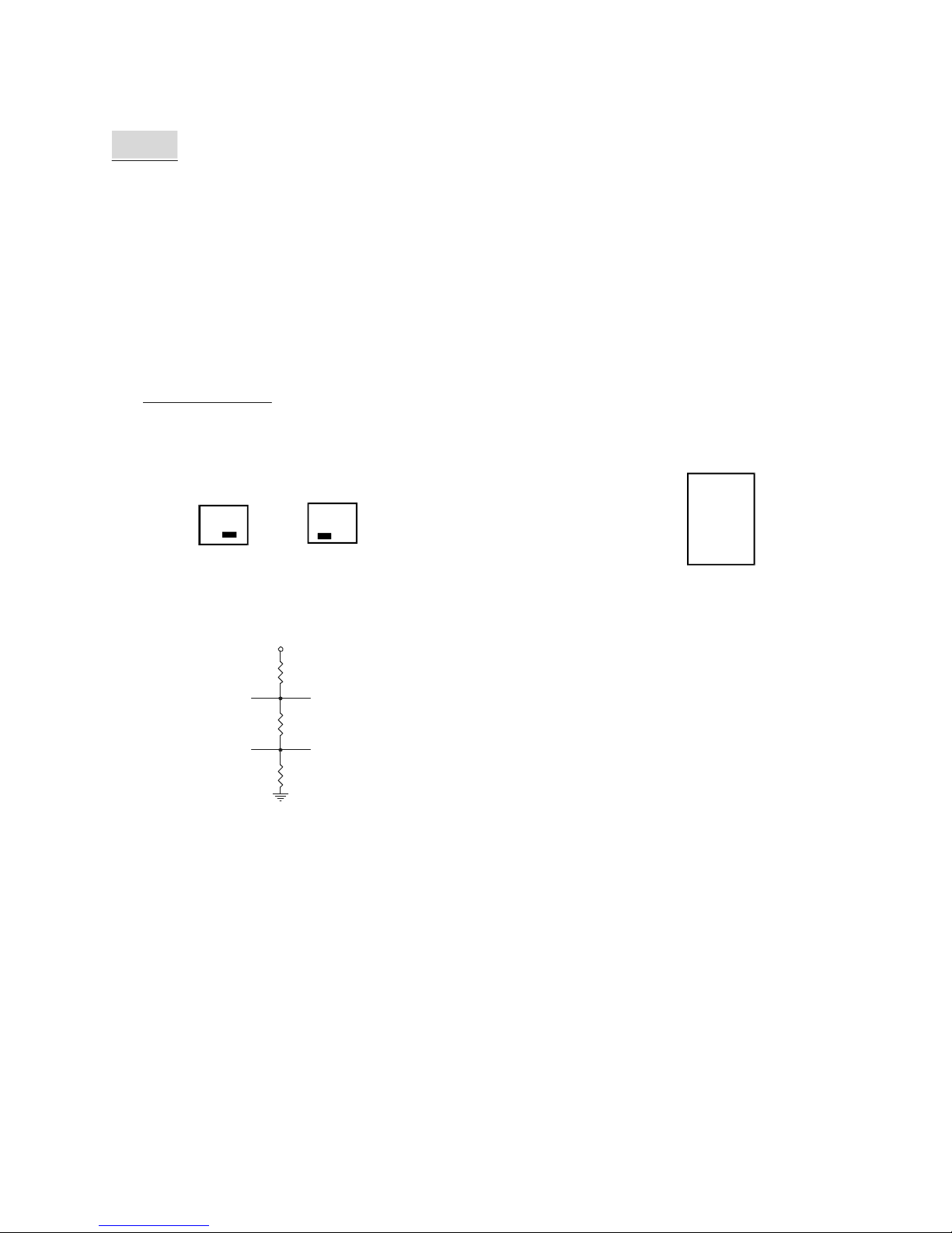
2.9.2 RS- 485 Mode Con figu ra tion
The RS- 485 Multi- drop in ter face is sup ported on both chan nels with the in stal la tion of the op tional
“Chip Kit”, Win Sys tems’ part number CK- 75176-2. A sin gle kit is suf fi cient to con fig ure both chan nels for RS- 485. RS- 485 is a 2- wire multi- drop in ter face where only one sta tion at a time talks (trans mits) while all oth ers lis ten (re ceive). RS- 485 usu ally re quires the twisted pair be ter mi n ated at each end
of the run. The re quired ter mi na tion val ues are de pend ent upon a number of fac tors in clud ing: line im ped ance, line length, etc. A good trial value is 100 ohms in all three re sis tor lo ca tions. The fol low ing il lus tra tions show the cor rect jump er ing, driver IC in stal la tion, I/O con nec tor pin out, and ter mi na tion
re sis tor lo ca tions for each of the chan nels when used in RS- 485 mode.
COM1 - RS- 485
COM1 DB9
J15 J17
3 2 1
o o o
VCC
R106
R109
R108
1 2 3
o o o
TX/RX-
TX/RX+
U4 - Not In stalled
U9 - In stalled
U5 - Not In stalled
N/C
TX/RX+
TX/RX-
N/C
GND
1 o o 6
2 o o 7
3 o o 8
4 o o 9
5 o
N/C
N/C
N/C
N/C
RS- 485 NOTE : Be cause RS- 485 uses a sin gle
twisted- pair, all trans mit ters are con nected in par al lel. Only one sta tion at a time may trans mit or have
its trans mit ter en abled. The trans mit ter En able/Dis able is con trolled in soft ware us ing bit 1 in the Mo dem Con trol Reg is ter (RTS). When RTS is set, the
trans mit ter is en abled, and when cleared (the nor mal
state) the trans mit ter is dis abled and the re ceiver is
en abled. Note that it is nec es sary to al low some
mini mal set tling time af ter ena bling the trans mit ter
bef ore trans mit ting the first char ac ter. Like wise, fol low ing a trans mis sion, it is nec es sary to be sure that
all char ac ters have been com pletely shifted out of
the UART (Check Bit 6 in the Line Status Reg is ter)
bef ore dis abling the trans mit ter to avoid chop ping
off the last char ac ter.
Im por tant Note: All se rial ter mi na tion com po nents are sur face mount 0805 pack ages on the
bot tom of the board. These should only be in stalled by sur face mount quali fied in di vidu als.
030923 OPERATIONS MANUAL EBC-BX Page 2 - 9
Page 17
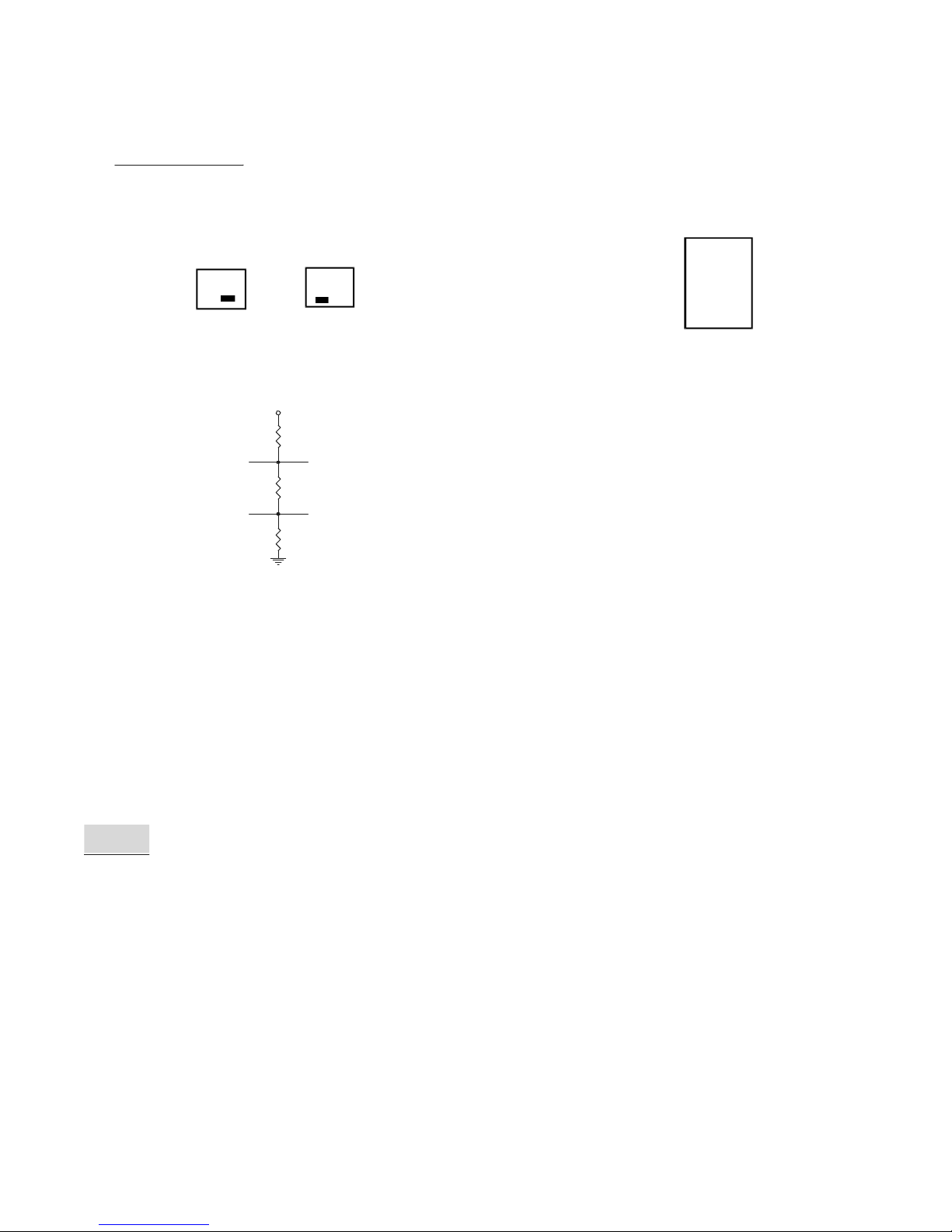
COM2 - RS- 485
WinSystems - "The Embedded Systems Authority"
COM2 DB9
J16 J18
3 2 1
o o o
VCC
R103
R105
R104
1 2 3
o o o
TX/RX-
TX/RX+
U6 - Not In stalled
U10 - In stalled
U7 - Not In stalled
N/C
TX/RX+
TX/RX-
N/C
GND
1 o o 6
2 o o 7
3 o o 8
4 o o 9
5 o
N/C
N/C
N/C
N/C
RS- 485 NOTE : Be cause RS- 485 uses a sin gle
twisted- pair, all trans mit ters are con nected in par al lel. Only one sta tion at a time may trans mit or have
its trans mit ter en abled. The trans mit ter En able/Dis able is con trolled in soft ware us ing bit 1 in the Mo dem Con trol Reg is ter (RTS). When RTS is set, the
trans mit ter is en abled, and when cleared (the nor mal
state) the trans mit ter is dis abled and the re ceiver is
en abled. Note that it is nec es sary to al low some
mini mal set tling time af ter ena bling the trans mit ter
bef ore trans mit ting the first char ac ter. Like wise, fol low ing a trans mis sion, it is nec es sary to be sure that
all char ac ters have been com pletely shifted out of
the UART (Check Bit 6 in the Line Status Reg is ter)
bef ore dis abling the trans mit ter to avoid chop ping
off the last char ac ter.
Im por tant Note : All se rial ter mi na tion com po nents are sur face mount 0805 pack ages. These
should only be in stalled by sur face mount quali fied in di vidu als.
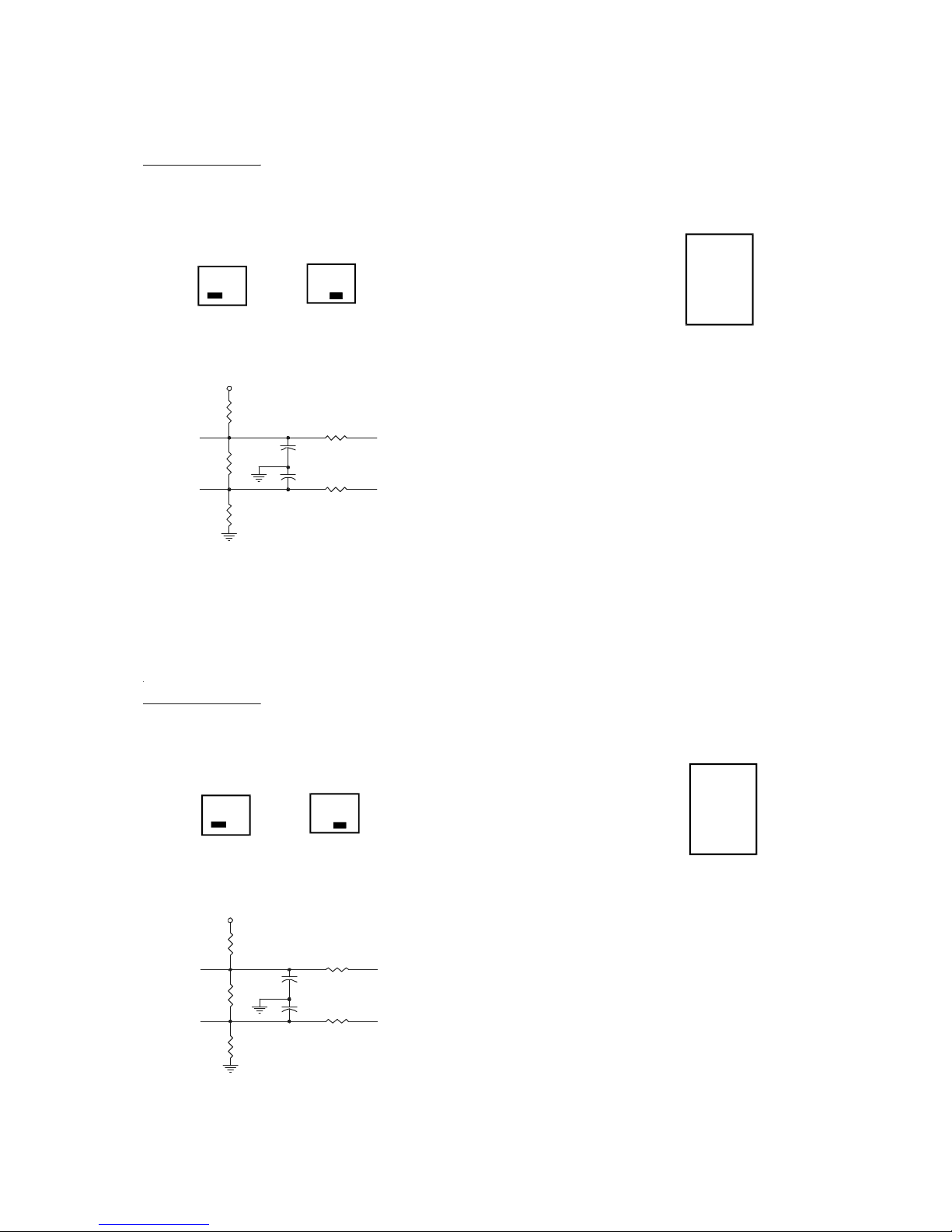
2.9.3 SAE J1708 Con figu ra tion
The So ci ety of Auto mo tive En gi neers (SAE) J1708 in ter face is a varia tion of the RS- 485 in ter face
which is used for “Se rial Data Com mu ni ca tions be tween Mi cro com puter Sys tems in Heavy Duty Ve hi cle Ap pli ca tions”. It is be yond the scope of this docu ment to go into de tail on the J1708 speci fi ca tion.
The EBC- BX may be user con fig ured for J1708 by the ad di tion of the CK- 75176-2 “Chip Kit”. One
“Chip Kit” is suf fi cient to con fig ure both chan nels for J1708. The il lus tra tions that fol l ow show the cor rect jump er ing, driver IC in stal la tion, I/O con nec tor pin defi ni tions, and the ter mi na t ion net work de tails
for each of the chan nels when used in J1708 mode.
Page 2 - 10 OPERATIONS MANUAL EBC-BX 030923
Page 18
COM1 - J1708
WinSystems - "The Embedded Systems Authority"
COM1 DB9
R106
4.7K
R109
Absent
R108
4.7K
J15 J17
3 2 1
o o o
VCC
1 2 3
o o o
R111 47 OHM
C104 .0022 ufd
C103 .0022 ufd
R110 47 OHM
U4 - Not In stalled
U9 - In stalled
U5 - Not In stalled
TX/RX+
TX/RX-
TX/RX+
TX/RX-
GND
N/C
N/C
1 o o 6
2 o o 7
3 o o 8
4 o o 9
5 o
N/C
N/C
N/C
N/C
Im por tant Note : All se rial ter mi na tion com po nents are sur face mount 0805 pack ages on the
bot tom of the board. These should only be in stalled by sur face mount quali fied in di vidu als.
COM2 - J1708
J16 J18
3 2 1
o o o
VCC
R103
4.7K
R1105
Absent
R104
4.7K
1 2 3
o o o
R100 47 OHM
C100 .0022 ufd
C101 .0022 ufd
R101 47 OHM
U6 - Not In stalled
U10 - In stalled
U7 - Not In stalled
TX/RX+
TX/RX-
N/C
TX/RX+
TX/RX-
N/C
GND
COM2 DB9
1 o o 6
2 o o 7
3 o o 8
4 o o 9
5 o
N/C
N/C
N/C
N/C
030923 OPERATIONS MANUAL EBC-BX Page 2 - 11
Page 19

WinSystems - "The Embedded Systems Authority"
2.10 Par al lel Printer Port
The EBC- BX sup ports a fully bi- directional par al lel printer port ca pa ble of EPP and ECP op e ra -
tions. The PnP par al lel port is mapped by de fault at 378H and is ter mi nated at the Multi-I/O con nec tors
at J3. Other I/O and in ter rupt map ping are avail able us ing the Award BIOS setup menu op tions. The pin
defi ni tions for the par al lel port DB25 con nec tor when us ing the CBL- 247-1 ca ble are shown be low:
PD0
PD1
PD2
PD3
PD4
PD5
PD6
PD7
ACK
PE
SLCT
1 o o 14
2 o o 15
3 o o 16
4 o o 17
5 o o 18
6 o o 19
7 o o 20
8 o o 21
9 o o 22
10 o o 23
11 o o 24
12 o o 25
13 o
AUTOFD
ERROR
INIT
SLIN
GND
GND
GND
GND
GND
GND
GND
GND
STROBE
BUSY
2.11 Speaker/Sound In ter face
The EBC- BX util izes a high- impedance piezo type de vice for audio out put. BIOS beep codes, er r or
sig nal ing, or user- defined tones can be pre sented via this de vice.
2.12 PC/104 Bus In ter face
The EBC- BX sup ports I/O ex pan sion through the stan dard PC/104 con nec tors at J20 and J23. The
EBC- BX sup ports both 8- bit and 16- bit PC/104 mod ules. The PC/104 con nec tor pin defi ni tions are
pro vided on the fol low ing page for ref er ence pur poses.
Page 2 - 12 OPERATIONS MANUAL EBC-BX 030923
Page 20

WinSystems - "The Embedded Systems Authority"
GND
RESET
+5V
IRQ9
-5V
DRQ2
-12V
0WS
+12V
GND
MEMW
MEMR
IOW
IOR
DACK3
DRQ3
DACK1
DRQ1
REFRESH
SYSCLK
IRQ7
IRQ6
IRQ5
IRQ4
IRQ3
DACK2
TC
BALE
+5V
OSC
GND
GND
J23
B1 o o A1
B2 o o A2
B3 o o A3
B4 o o A4
B5 o o A5
B6 o o A6
B7 o o A7
B8 o o A8
B9 o o A9
B10 o o A10
B11 o o A11
B12 o o A12
B13 o o A13
B14 o o A14
B15 o o A15
B16 o o A16
B17 o o A17
B18 o o A18
B19 o o A19
B20 o o A20
B21 o o A21
B22 o o A22
B23 o o A23
B24 o o A24
B25 o o A25
B26 o o A26
B27 o o A27
B28 o o A28
B29 o o A29
B30 o o A30
B31 o o A31
B32 o o A32
IOCHK
BD7
BD6
BD5
BD4
BD3
BD2
BD1
BD0
IOCHRDY
AEN
SA19
SA18
SA17
SA16
SA15
SA14
SA13
SA12
SA11
SA10
SA9
SA8
SA7
SA6
SA5
SA4
SA3
SA2
SA1
SA0
GND
GND
SBHE
LA23
LA22
LA21
LA20
LA19
LA18
LA17
MEMR
MEMW
SD8
SD9
SD10
SD11
SD12
SD13
SD14
SD15
KEY
J20
C0 o o D0
C1 o o D1
C2 o o D2
C3 o o D3
C4 o o D4
C5 o o D5
C6 o o D6
C7 o o D7
C8 o o D8
C9 o o D9
C10 o o D10
C11 o o D11
C12 o o D12
C13 o o D13
C14 o o D14
C15 o o D15
C16 o o D16
C17 o o D17
C18 o o D18
C19 o o D19
GND
MEMCS16
IOCS16
IRQ10
IRQ11
IRQ12
IRQ15
IRQ14
DACK0
DRQ0
DACK5
DRQ5
DACK6
DRQ6
DACK7
DRQ7
VCC
MASTER
GND
GND
2.13 PC/104Plus Bus In ter face
The EBC- BX sup ports I/O ex pan sion through the stan dard PC/104Plus con nec tor at J22. The
PC/104Plus Bus pin defi ni tions are pro vided on the fol low ing page for ref er ence pur poses.
030923 OPERATIONS MANUAL EBC-BX Page 2 - 13
Page 21

WinSystems - "The Embedded Systems Authority"
J22
Pin A B C D
1 GND/5.0 KEY Re served +5 AD00
2 VI/O AD02 AD01 +5V
3 AD05 GND AD04 AD03
4 C/BE0* AD07 GND AD06
5 GND AD09 AD08 GND
6 AD11 VI/O AD10 M66EN
7 AD14 AD13 GND AD06
8 +3.3V C/BE1* AD15 +3.3V
9 SERR* GND SB0* PAR
10 GND PERR* +3.3V SDONE
11 STOP* +3.3V LOCK* GND
12 +3.3V TRDY* GND DEVSEL*
13 FRAME* GND IRDY* +3.3V
14 GND AD16 +3.3.V
15 AD18 +3.3V AD17 GND
16 AD21 AD20 GND AD19
17 +3.3V AD23 AD22 +3.3V
18 ID SEL0 GND ID SEL1 ID SEL2
19 AD24 C/BE3* VI/O ID SEL3
20 GND AD26 AD25 GND
21 AD29 +5V AD28 AD27
22 +5V AD30 GND AD31
23 REQ0* GND REQ1* VI/O
24 GND REQ2* +5V GNT0*
25 GNT1* VI/O GNT2* GND
26 +5V CLK0 GND CLK1
27 CLK2 +5V CLK3 GND
28 GND INTD* +5V RST*
29 +12V INTA* INTB* INTC*
30 -12V Re served Re served GND/3.3V KEY
C/BE3*
2.14 Floppy Disk In ter face
The EBC- BX sup ports up to 2 stan dard 3 1/2" or 5 1/4" PC com pati ble floppy disk drives. The
drives are con nected via the I/O con nec tor at J10. Note that the in ter con nect ca ble to the drives is a stan dard floppy I/O ca ble used on desk top PCs. The ca ble must have the twisted sec tion prior to the drive A
po si tion. The pin defi ni tions for the J10 con nec tor are shown on the fol low ing page:
Page 2 - 14 OPERATIONS MANUAL EBC-BX 030923
Page 22

WinSystems - "The Embedded Systems Authority"
J10
GND
GND
GND
GND
GND
GND
GND
GND
GND
GND
GND
GND
GND
GND
GND
GND
GND
1 o o 2
3 o o 4
5 o o 6
7 o o 8
9 o o 10
11 o o 12
13 o o 14
15 o o 16
17 o o 18
19 o o 20
21 o o 22
23 o o 24
25 o o 26
27 o o 28
29 o o 30
31 o o 32
33 o o 34
RPM/LC
N/C
N/C
INDEX
MTR0
DRV1
DRV0
MTR1
DIR
STEP
WDATA
WGATE
TRK0
WPRT
RDATA
HDSEL
DSKCHG
2.15 IDE Hard Disk In ter face
The EBC- BX sup ports stan dard IDE fixed disks through the I/O con nec tors at J5 (pri mary) and J8
(sec on dary). The EBC- BX sup ports mul ti ple PIO modes as well as Ultra- DMA (UDMA)33 and
UDMA 66 drives when used with an UDMA 80- pin ca ble (Win Sys tems P/N CBL- 126- 10). A red ac tiv ity LED is pres ent at D3 and D2 for the pri mary and sec on dary hard drive con trol lers re s pec tively.
The pin defi ni tions for J5 and J8 are shown here:
RST
D7
D6
D5
D4
D3
D2
D1
D0
LED
DRQ
IOW
IOR
RDY
DACK
IRQ
A1
A0
CS1
VCC
J5 and J8
1 o o 2
3 o o 4
5 o o 6
7 o o 8
9 o o 10
11 o o 12
13 o o 14
15 o o 16
17 o o 18
19 o o 20
21 o o 22
23 o o 24
25 o o 26
27 o o 28
29 o o 30
31 o o 32
33 o o 34
35 o o 36
37 o o 38
39 o o 40
GND
D8
D9
D10
D11
D12
D13
D14
D15
N/C
GND
GND
GND
NC
GND
NC
NC
A2
CS3
GND
030923 OPERATIONS MANUAL EBC-BX Page 2 - 15
Page 23
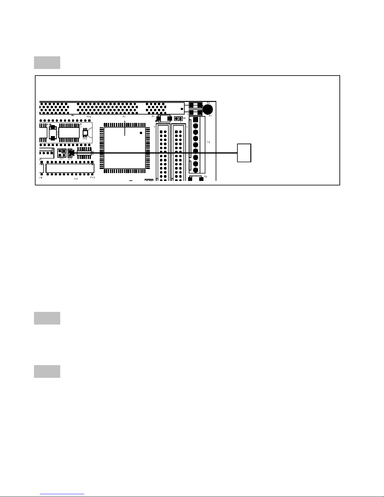
WinSystems - "The Embedded Systems Authority"
2.16 Watch dog Timer Con figu ra tion
Watch dog Timer con figu ra tion jumper J21
J21
1 o
2 o
The EBC- BX board fea tures a power- on volt age de tect, and power- down/power brown out re set
cir cuit to pro tect mem ory and I/O from faulty CPU op era tion dur ing pe ri ods of il le gal volt age lev els.
This su per vi sor cir cuitry also fea tures a watch dog timer which can be used to guard against soft ware
lock ups. An in ter nal timer with a pe ri od of 1.5 or 150 sec onds will, when en abled, re set the CPU if the
watch dog has not been serv iced within the al lot ted time. The watch dog timer powers- up dis abled and
must be en abled in soft ware bef ore tim ing will be gin. Ena bling is ac com plished by writ ing a 1 to I/O
port 1EEH. Writ ing a 0 to I/O port 1EEH will dis able the watch dog. Af ter ena bling, pet ting may be ac com plished by writ ing any value to I/O port 1EFH at least every 1.5 if J21 is not jumpered or at least
every 150 sec onds if J21 is jumpered, or a re set will oc cur. This mode of op era tion can be used with the
BIOS or DOS pro vided that the watch dog is dis abled bef ore mak ing any ex ten sive BIOS or DOS calls,
es pe cially video or disk I/O calls which could ex ceed the time sec onds al lowed when the 1.5 sec ond
mode is used.
2.17 Status LED
A green LED is popu lated on the board at D1 which can be used for any ap pli ca tion spe cific pur -
pose. The LED can be turned on in soft ware by writ ing a 1 to I/O port 1EDH. The LED can be turned off
by writ ing a 0 to 1EDH.
2.18 Bat tery Se lect Con trol
An on board 350mAH nomi nal ca pac ity, lith ium bat tery is pro vided for the CMOS Clock/Cal en dar.
A mas ter bat tery en able jumper is pro vided at J27. When J27 is jumpered pins 2-3, bat tery power is
sup plied to the Clock/Cal en dar. When J27 is jumpered pins 1-2, the bat tery is to tally dis con nected and
no cur rent will be drawn from it. Bat tery life is highly de pend ent upon duty cy cle as there is no cur rent
drawn from the bat tery when +5 volts is ap plied to the board. Both stor age and op era tional tem pera tures
play a promi nent fac tor in bat tery life. High tem pera tures will shorten bat tery life sig nifi cantly. J27
must be jumpered 1-2 if a bat tery is not in stalled.
Page 2 - 16 OPERATIONS MANUAL EBC-BX 030923
Page 24
WinSystems - "The Embedded Systems Authority"
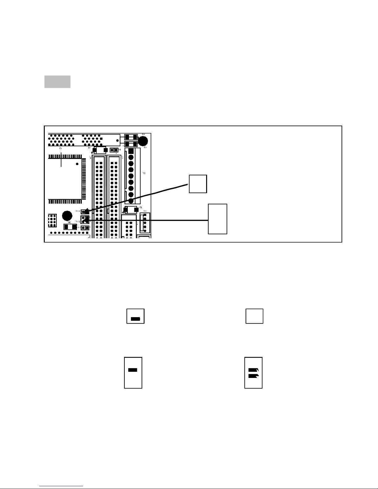
2.19 Disk On Chip Con figu ra tion
The Disk On Chip can be en abled by jump er ing J12 and J13 as shown be low.
J12
2 1
o o
J13
3 1
o o
o o
4 2
J12 DOC En able Jumper
J13 DOC Win dow Se lect
BIOS Write Enable
Note : J13 pins 1-2 con trol BIOS write, and must be jumpered at all times for proper
Plug- N- Play op era tion.
J12
2 1
o o
DiskOnChip Enabled
J13
2 1
o o
o o
4 3
DOC at D800:0000
DiskOnChip Disabled
DOC at D000:0000
J12
2 1
o o
J13
2 1
o o
o o
4 3
030923 OPERATIONS MANUAL EBC-BX Page 2 - 17
Page 25
WinSystems - "The Embedded Systems Authority"
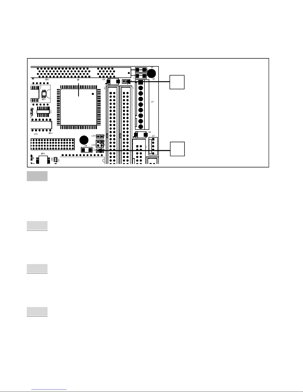
J6
2 1
o o
J6 Par al lel I/O En able
J14 Par al lel I/O +5V Supply Enable
J14
2 1
o o
2.20 Par al lel I/O
The EBC- BX util izes the Win Sys tems WS16C48 ASIC high- density I/O chip mapped at a base ad -
dress of 120H. The first 24 lines are ca pa ble of fully latched event sens ing with sense po lar i ty be ing
soft ware pro gram ma ble. Two, 50- pin con nec tors al low for easy mat ing with in dus try stan d ard I/O
racks. The pin out for the two con nec tors are shown on the next page.
2.20.1 Par al lel I/O En able
The par al lel fea tures of the EBC- BX can be en abled or dis abled us ing the jumper block at J6. When
J6 is jumpered the par al lel I/O is en abled at I/O ad dress 120H. When J6 is open the 16 ad dresses start ing
at I/O ad dress 120H are free for use by other de vices.
2.20.2 Par al lel I/O VCC En able
The I/O con nec tors can pro vide +5 volts to an I/O rack or for mis cel la ne ous pur poses by jump er ing
J14. When J14 is jumpered +5 volts is pro vided at pin 49 of both J7 and J9. It the user's re spon si bil ity to
limit cur rent to a safe value (less than 400mA ) to avoid dam ag ing the CPU board.
2.20.3 Par al lel I/O Con nec tors
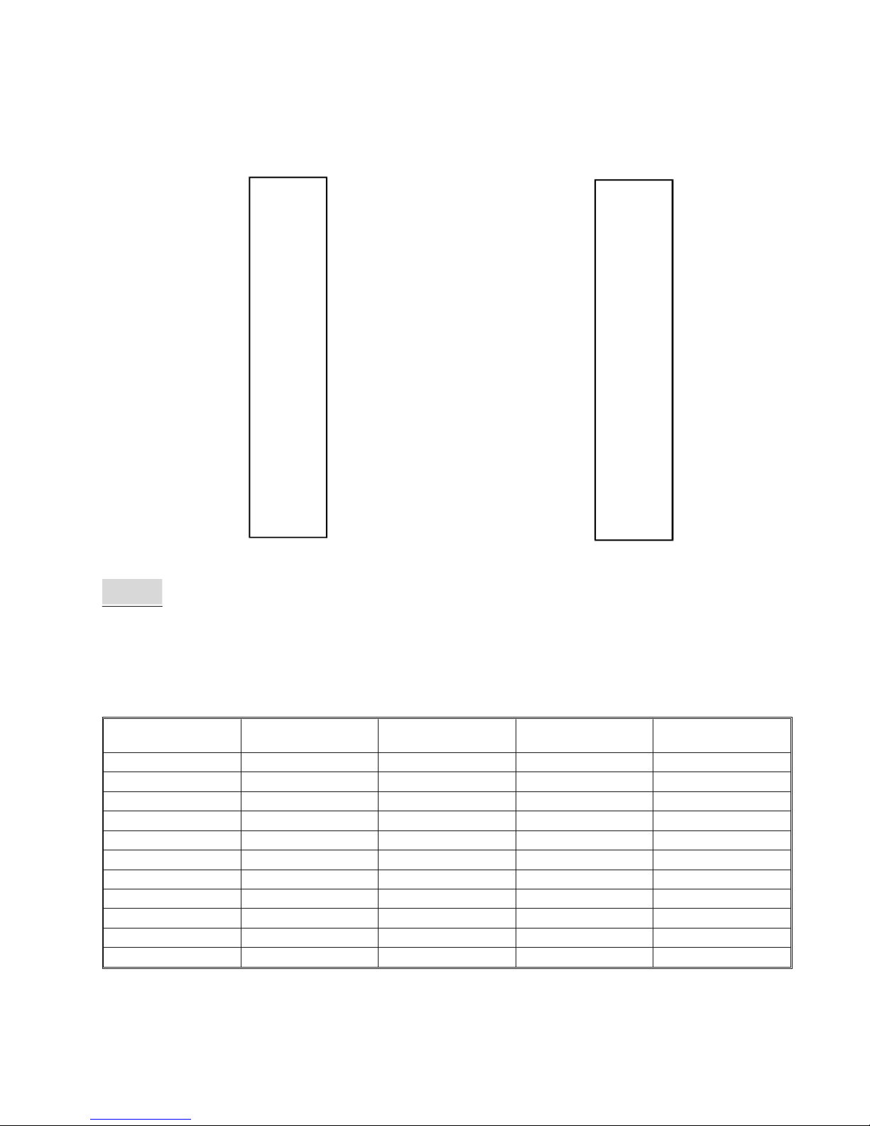
The 48 lines of par al lel I/O are ter mi nated through two 50- pin con nec tors at J7 and J9. The J7 con -
nec tor han dles I/O ports 0-2 while J9 han dles ports 3-5. The pin defi ni tions for J7 and J9 are shown on
the fol low ing page.
Page 2 - 18 OPERATIONS MANUAL EBC-BX 030923
Page 26
WinSystems - "The Embedded Systems Authority"
Port 2 Bit 7
Port 2 Bit 6
Port 2 Bit 5
Port 2 Bit 4
Port 2 Bit 3
Port 2 Bit 2
Port 2 Bit 1
Port 2 Bit 0
Port 1 Bit 7
Port 1 Bit 6
Port 1 Bit 5
Port 1 Bit 4
Port 1 Bit 3
Port 1 Bit 2
Port 1 Bit 1
Port 1 Bit 0
Port 0 Bit 7
Port 0 Bit 6
Port 0 Bit 5
Port 0 Bit 4
Port 0 Bit 3
Port 0 Bit 2
Port 0 Bit 1
Port 0 Bit 0
+5V
J7
1 o o 2
3 o o 4
5 o o 6
7 o o 8
9 o o 10
11 o o 12
13 o o 14
15 o o 16
17 o o 18
19 o o 20
21 o o 22
23 o o 24
25 o o 26
27 o o 28
29 o o 30
31 o o 32
33 o o 34
35 o o 36
37 o o 38
39 o o 40
41 o o 42
43 o o 44
45 o o 46
47 o o 48
49 o o 50
GND
GND
GND
GND
GND
GND
GND
GND
GND
GND
GND
GND
GND
GND
GND
GND
GND
GND
GND
GND
GND
GND
GND
GND
GND
Port 5 Bit 7
Port 5 Bit 6
Port 5 Bit 5
Port 5 Bit 4
Port 5 Bit 3
Port 5 Bit 2
Port 5 Bit 1
Port 5 Bit 0
Port 4 Bit 7
Port 4 Bit 6
Port 4 Bit 5
Port 4 Bit 4
Port 4 Bit 3
Port 4 Bit 2
Port 4 Bit 1
Port 4 Bit 0
Port 3 Bit 7
Port 3 Bit 6
Port 3 Bit 5
Port 3 Bit 4
Port 3 Bit 3
Port 3 Bit 2
Port 3 Bit 1
Port 3 Bit 0
+5V
J9
1 o o 2
3 o o 4
5 o o 6
7 o o 8
9 o o 10
11 o o 12
13 o o 14
15 o o 16
17 o o 18
19 o o 20
21 o o 22
23 o o 24
25 o o 26
27 o o 28
29 o o 30
31 o o 32
33 o o 34
35 o o 36
37 o o 38
39 o o 40
41 o o 42
43 o o 44
45 o o 46
47 o o 48
49 o o 50
GND
GND
GND
GND
GND
GND
GND
GND
GND
GND
GND
GND
GND
GND
GND
GND
GND
GND
GND
GND
GND
GND
GND
GND
GND
2.20.4 WS16C48 Reg is ter Defi ni tions
The EBC- BX uses the Win Sys tems ex clu sive ASIC de vice, the WS16C48. This de vice pro vides 48
lines of digi tal I/O. There are 17 unique reg is ters within the WS16C48. The fol low ing ta ble sum ma rizes the reg is ters and the text that fol lows pro vides de tails on each of the in ter nal reg i s ters.
I/O Ad dress
Off set
00H Port 0 I/O Port 0 I/O Port 0 I/O Port 0 I/O
01H Port 1 I/O Port 1 I/O Port 1 I/O Port 1 I/O
02H Port 2 I/O Port 2 I/O Port 2 I/O Port 2 I/O
03H Port 3 I/O Port 3 I/O Port 3 I/O Port 3 I/O
04H Port 4 I/O Port 4 I/O Port 4 I/O Port 4 I/O
05H Port 5 I/O Port 5 I/O Port 5 I/O Port 5 I/O
06H Int_Pend ing Int_Pend ing Int_Pend ing Int_Pend ing
07H Page/Lock Page/Lock Page/Lock Page/Lock
08H N/A Pol_0 Enab_0 Int_ID0
09H N/A Pol_1 Enab_1 Int_ID1
0AH N/A Pol_2 Enab_2 Int_ID2
Page 0 Page 1 Page 2 Page 3
030923 OPERATIONS MANUAL EBC-BX Page 2 - 19
Page 27

WinSystems - "The Embedded Systems Authority"
Reg is ter De tails
Port 0-5 I/O - Each I/O bit in each of the 6 ports can be in di vidu ally pro grammed for in put or out -
put. Writ ing a '0' to a bit po si tion causes the cor re spond ing out put pin to go to a High- Impedance state
(pulled high by ex ter nal 10K ohm re sis tors). This al lows it to be used as an in put. When used in the in put
mode, a read re flects the in verted state of the I/O pin, such that a high on the pin will read as a '0' in the
reg is ter. Writ ing a '1' to a bit po si tion causes the out put pin to sink cur rent (up to 12mA), ef fec tively
pull ing it low.
INT_PEND ING - This read- only reg is ter re flects the com bined state of the INT_ID0 through
INT_ID2 reg is ters. When any of the lower 3 bits are set, it in di cates that an in ter rupt is pend ing on the
I/O port cor re spond ing to the bit po si tion(s) that are set. Read ing this reg is ter al lows an In ter rupt Serv ice Rou tine to quickly de ter mine if any in ter rupts are pend ing and which I/O port has a pend ing in ter rupt.
PAGE/LOCK - This reg is ter serves two pur poses. The up per two bits se lect the reg is ter page in use
as shown here:
D7 D6 Page
0 0 Page 0
0 1 Page 1
1 0 Page 2
1 1 Page 3
Bits 5-0 al low for lock ing the I/O ports. A '1' writ ten to the I/O port po si tion will pro hibit fur ther
writes to the cor re spond ing I/O port.
POL0- POL2 - These reg is ters are ac ces si ble when page 1 is se lected. They al low in ter rupt po lar ity
se lec tion on a port- by- port and bit- by- bit ba sis. Writ ing a '1' to a bit po si tion se lects the ris ing edge de tec tion in ter rupts while writ ing a '0' to a bit po si tion se lects fal ling edge de tec tion in ter rupts.
ENAB0- ENAB2 - These reg is ters are ac ces si ble when page 2 is se lected. They al low for port- by-
port and bit- by- bit ena bling of the edge de tec tion in ter rupts. When set to a '1' the edge de tec tion in ter rupt is en abled for the cor re spond ing port and bit. When cleared to a '0', the bit's edge de tec tion in ter rupt
is dis abled. Note that this reg is ter can be used to in di vidu ally clear a pend ing in ter rupt by dis abling and
reena bling the pend ing in ter rupt.
INT_ID0 - INT_ID2 - These reg is ters are ac ces si ble when page 3 is se lected. They are used to
iden tify cur rently pend ing edge in ter rupts. A bit when read as a '1' in di cates that an edge of the po lar ity
pro grammed into the cor re spond ing po lar ity reg is ter has been rec og nized. Note that a write to this reg is ter (value ig nored) clears ALL of the pend ing in ter rupts in this reg is ter.
Page 2 - 20 OPERATIONS MANUAL EBC-BX 030923
Page 28

WinSystems - "The Embedded Systems Authority"
2.21 VGA Con figu ra tion
The EBC- BX uses a fourth gen era tion CRT/Flat panel Su per VGA con trol ler. It sup ports stan dard
VGA out put as well as a va ri ety of Flat Panel Dis plays us ing op tional Flat Panel Adapter (FPA) kits.
The video on the EBC- BX uses the Asil iant 69000 se ries VGA con trol lers. The Asili ant con trol ler sup ports stan dard and super- VGA as well as Color and Mono chrome pan els with 8, 9, 12, 15, 16, 18, 24 and
36- bit in ter faces.
Win Sys tems pro vides flat panel sup port through a se ries of Flat Panel Adapter (FPA) kits. Con tact
your Win Sys tems Ap pli ca tions En gi neer for the most cur rent list of avail able FPA’s and sup ported
pan els.De tails re gard ing in ter fac ing to spe cific Flat Pan els is not pro vided in this man ual but should be
ref er enced in the docu men ta tion ac com pa ny ing the FPA kit. At tempted con nec tion to any flat panel not
di rectly sup ported by a Win Sys tems FPA mod ule is at the us er’s risk and ex treme care should be ex er cised to avoid dam ag ing or de stroy ing the panel.
HAZ ARD WARN ING: LCD pan els can re quire a high volt age for the panel back light. This high frequency volt age can ex ceed 1000 volts and can pres ent a shock haz ard. Care should be taken when
wir ing or han dling the inverter out put. To avoid dan ger of shock and to avoid dam ag ing frag i le and ex pen sive pan els, make all con nec tion changes with power re moved.
Note: J26 must be jumpered 1-2 for Sharp-type pan els, and 2-3 for NEC-type pan els.
2.21.1 CRT Out put Con nec tion
Video out put to a stan dard VGA moni tor is made via the con nec tor at J32. An adapter ca ble part
number CBL- 234-1 is avail able from Win Sys tems to adapt from J32 to the stan dard DB15 VGA con nec tor. The pin defi ni tions for the J32 con nec tor are shown here :
J32
RED
GREEN
BLUE
HSYNC
VSYNC
DDCDATA
DDCCLK
1 o o 2
3 o o 4
5 o o 6
7 o o 8
9 o o 10
11 o o 12
13 o o 14
GND
GND
GND
GND
GND
GND
VCC
030923 OPERATIONS MANUAL EBC-BX Page 2 - 21
Page 29
WinSystems - "The Embedded Systems Authority"
2.21.2 Panel Back light Con nec tion
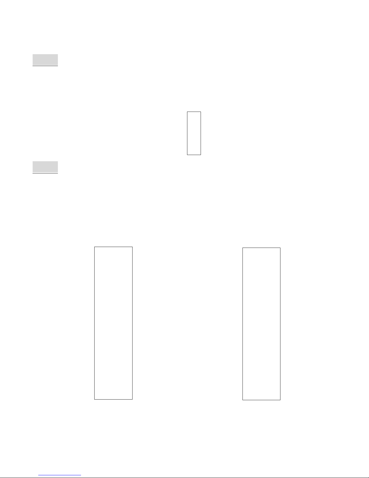
Panel Back light con nec tion is made via the con nec tor at J25. The pinout for J25 is shown here for
reference.
J25
o 1
+12
o 2
+12
o 3
GND
o 4
GND
VCC
VCC
o 5
o 6
o 7
ENBKL
2.21.3 Flat Panel Out put Con nec tion
Con nec tion to all flat pan els is made via the two 50- pin con nec tors at J31 and J32. These con nec tors
are ca bled to the ap pro pri ate FPA (Flat Panel Adapter) mod ule which then breaks out the nec e s sary ca bling for at tach ment to the panel it self. The FPA mod ule also sup plies any spe cial con trols that may be
needed for the panel. Ref er to the FPA docu men ta tion for spe cific hookup in struc tions. The pin defi ni tions for J30 and J33 are shown here :
FP12
FP13
FP14
FP15
FP16
FP17
FP18
FP19
FP20
FP21
FP22
FP23
FP24
FP25
FP26
FP27
FP28
FP29
FP30
FP31
FP32
FP33
FP34
FP35
SWVCC
J30
1 o o 2
3 o o 4
5 o o 6
7 o o 8
9 o o 10
11 o o 12
13 o o 14
15 o o 16
17 o o 18
19 o o 20
21 o o 22
23 o o 24
25 o o 26
27 o o 28
29 o o 30
31 o o 32
33 o o 34
35 o o 36
37 o o 38
39 o o 40
41 o o 42
43 o o 44
45 o o 46
47 o o 48
49 o o 50
GND
GND
GND
GND
GND
GND
GND
GND
GND
GND
GND
GND
GND
GND
GND
GND
GND
GND
GND
GND
GND
GND
GND
GND
SWVCC
SW0
SW2
FPO
FP1
FP2
FP3
FP4
FP5
FP6
FP7
FP8
FP9
FP10
FP11
PCSHCLK
PCFLM
PCLP
PCM
PHSYNC
PVSYNC
ENVCC
ENBKL
ENVEE
+12V
SWVCC
J33
1 o o 2
3 o o 4
5 o o 6
7 o o 8
9 o o 10
11 o o 12
13 o o 14
15 o o 16
17 o o 18
19 o o 20
21 o o 22
23 o o 24
25 o o 26
27 o o 28
29 o o 30
31 o o 32
33 o o 34
35 o o 36
37 o o 38
39 o o 40
41 o o 42
43 o o 44
45 o o 46
47 o o 48
49 o o 50
SW1
SW3
GND
GND
GND
GND
GND
GND
GND
GND
GND
GND
GND
GND
GND
GND
GND
GND
GND
GND
GND
GND
-12V
+12V
SWVCC
Page 2 - 22 OPERATIONS MANUAL EBC-BX 030923
Page 30

WinSystems - "The Embedded Systems Authority"
2.21.4 Video Mode Ta ble
The EBC-BX video section supports a number of standard and extended VGA modes. The
following table extracted from the Asiliant 69000 databook shows the video modes supported.
Resolution Color depth (bpp) Re fresh Rates
640 x 480 8 60, 75, 85
640 x 480 16 60, 75, 85
640 x 480 24 60, 75, 85
800 x 600 8 60, 75, 85
800 x 600 16 60, 75, 85
800 x 600 24 60, 75, 85
1024 x 768 8 60, 75, 85
1024 x 768 16 60, 75, 85
1280 x 1024 8 60
2.22 Eth er net Con troller
The 82559 is part of In tel’s sec ond gen era tion fam ily of fully in te grated 10BASE-T/100BASE- TX
LAN so lu tions. The 82559 con sists of both the Me dia Ac cess Con trol ler (MAC) and the physi cal layer
(PHY) com bined into a sin gle com po nent so lu tion.
The 82559 is a 32- bit PCI con trol ler that fea tures en hanced scatter- gather bus mas ter ing ca pa bili ties which en ables it to per form high- speed data trans fers over the PCI bus. The 82559 bus mas ter ca pa bili ties en able the com po nent to pro cess high-level com mands and per form mul ti ple op era t ions off loading com mu ni ca tion tasks from the sys tem CPU. Two large trans mit and re ceive FI FOs of 3 Kbytes
each help pre vent data un derruns and over runs, al low ing the 82559 to trans mit data with mini mum in ter frame spac ing (IFS).
The 82559 can op er ate in ei ther full du plex or half du plex mode. In full du plex mode the 82559 ad heres to the IEEE 802.3x Flow Con trol speci fi ca tion. Half du plex per form ance is en hanced by a pro prie tary col li sion re duc tion mecha nism.
The 82559 in cludes a sim ple PHY in ter face to the wire trans former at rates of 10BASE-T and
100BASE- TX, and Auto- Negotiation ca pa bil ity for speed, du plex, and flow con trol. The 82559 also in cludes an in ter face to a se rial (4- pin) EE PROM. The EE PROM pro vides power- on ini tiali za t ion for
hard ware and soft ware con figu ra tion pa rame ters. The 82559 is also 100% PnP com pati ble and is con fig ured through this in ter face. Eth er net con nec tion to the EBC- BX is made through the con n ec tor at
J28.
There are Eth er net status LED’s at D6, D7, and D8. The color and func tion of each LED is listed be low :
D6 = Eth er net 100BASE- TX (Red)
D7 = Eth er net ac tiv ity LED (Green)
D8 = Eth er net link LED (Yel low)
For eth er net driv ers go to:
http://de vel oper.intel.com/design/network/drivers/
030923 OPERATIONS MANUAL EBC-BX Page 2 - 23
Page 31
WinSystems - "The Embedded Systems Authority"
Cool ing fan con nec tions J31 and J34
J34
3 o
2 o
1 o
J31
3 2 1
o o o
J31 and J34
GND
FAN POWER
FAN TACH
1 o
2 o
3 o
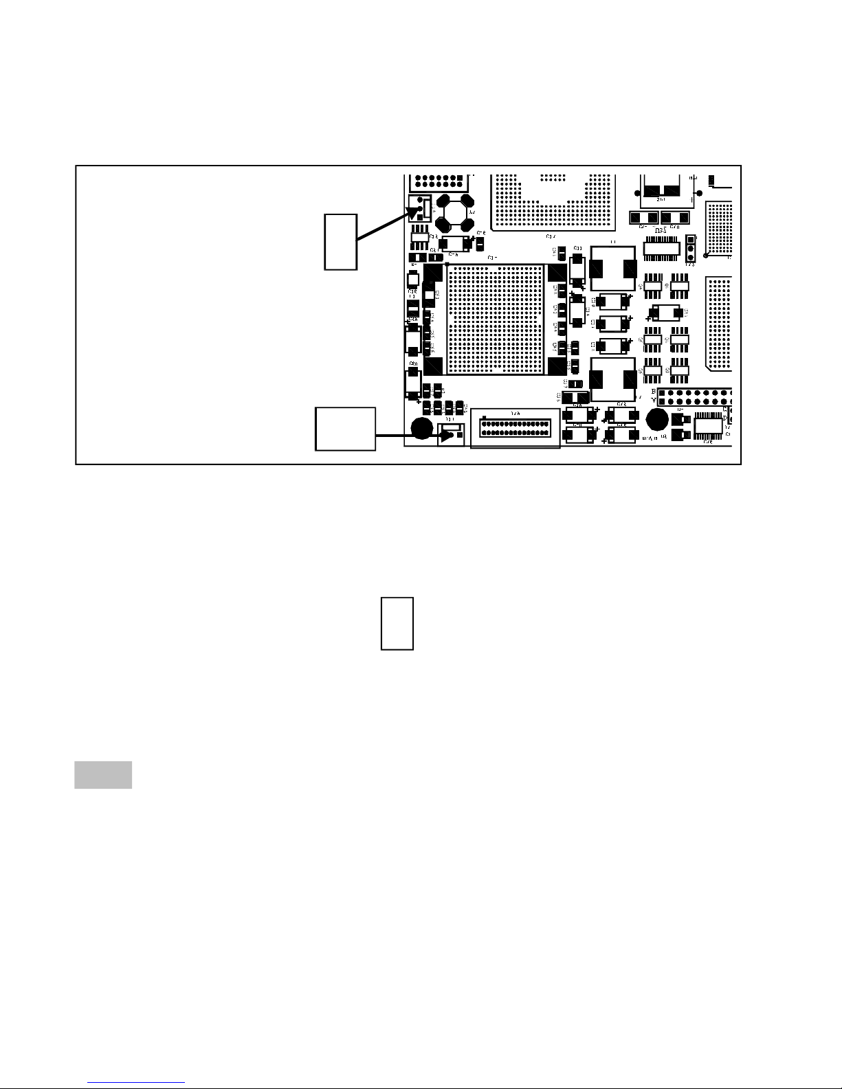
2.23 Fan Power Connector
The EBC- BX has a con nec tor lo cated at J31 to sup ply power to the proc es sor cool ing fan. The pin
de fi ni tions are shown here for ref er ence. There is also a con nec tor at J34 for use with an aux il iary sys tem cool ing fan. The pin defi ni tions for these con nec tors is shown here :
Both J31 and J34 pro vide +5V nomi nal at 250mA max.
Page 2 - 24 OPERATIONS MANUAL EBC-BX 030923
Page 32
WinSystems - "The Embedded Systems Authority"
2.24 Multi I/O Con nec tor
The I/O to the pri mary se rial chan nels, the printer port, and key board are all ter mi nated via the con nec tor at J2. An adapter ca ble, part number CBL- 247-1, is avail able from Win Sys tems to adapt to the
con ven tional I/O con nec tors. The pin defi ni tions for J2 are shown here
J2
COM1 - DCD
COM1 - RXD
COM1 - TXD
COM1 - DTR
COM1 - GND
COM2 - DSR
COM2 - RTS
COM2 - CTS
COM2 - RI
LPT - STROBE
LPT - PD0
LPT - PD1
LPT - PD2
LPT - PD3
LPT - PD4
LPT - PD5
LPT - PD6
LPT - PD7
LPT - ACK
LPT - BUSY
LPT - PE
LPT - SLCT
KEYBD - GND
KEYBD - KDATA
KEYBD - +5V
1 o o 2
3 o o 4
5 o o 6
7 o o 8
9 o o 10
11 o o 12
13 o o 14
15 o o 16
17 o o 18
19 o o 20
21 o o 22
23 o o 24
25 o o 26
27 o o 28
29 o o 30
31 o o 32
33 o o 34
35 o o 36
37 o o 38
39 o o 40
41 o o 42
43 o o 44
45 o o 46
47 o o 48
49 o o 50
COM1 - DSR
COM1 - RTS
COM1 - CTS
COM1 - RI
COM2 - DCD
COM2 - RSX
COM2 - TXD
COM2 - DTR
COM2 - GND
LPT - AUTOFD
LPT - ERROR
LPT - INIT
LPT - SLCTIN
LPT - GND
LPT - GND
LPT - GND
LPT - GND
LPT - GND
LPT - GND
LPT - GND
LPT - GND
KEYBD - GND
KEYBD - GND
KEYBD - CLK
KEYBD - +5V
2.25 USB Con nec tor
A USB cable may be attached via the connector at J11. An adapter cable, CBL-249-1 is available
from WinSystems to adapt to a conventional USB port. The pinout for J11 is shown here.
J11
USBV0
1 o
D0-
2 o
3 o
D0+
4 o
USBG0
030923 OPERATIONS MANUAL EBC-BX Page 2 - 25
Page 33

WinSystems - "The Embedded Systems Authority"
2.26 Jumper/Con nec tor Sum mary
Con nec tor/ De scrip tion Page Ref er ence
Jumper
J1 Mouse con nec tor 2-3
J2 Multi-I/O con nec tor 2-25
J3 Power con nec tor 2-3
J4 COM3, COM4 con nec tor 2-7
J5 Pri mary IDE con nec tor 2-15
J6 Par al lel I/O en able jumper 2-18
J7 Par al lel I/O con nec tor 2-18
J8 Sec on dary IDE con nec tor 2-15
J9 Par al lel I/O con nec tor 2-18
J10 Floppy disk con nec tor 2-14
J11 USB con nec tor 2-25
J12 DOC En able jumper 2-17
J13 DOC con figu ra tion jumper 2-17
J14 Par al lel I/O VCC se lect jumper 2-18
J15 COM1 RS- 422/RS- 485 con figu ra tion jumper 2-5
J16 COM2 RS- 422/RS- 485 con figu ra tion jumper 2-5
J17 COM1 RS- 422/RS- 485 con figu ra tion jumper 2-5
J18 COM1 RS- 422/RS- 485 con figu ra tion jumper 2-5
J19 IRQ rout ing jumper 2-2
J20 PC/104 16- bit con nec tor 2-13
J21 Watch dog Timer con figu ra tion jumper 2-16
J22 PC/104Plus con nec tor 2-13
J23 PC/104 8- bit con nec tor 2-13
J24 COM3/COM4 En able jumper 2-5
J25 Flat Panel back light con nec tor 2-22
J26 Flat Panel back light type se lect jumper 2-21
J27 Master Bat tery se lect jumper 2-4
J28 Eth er net con nec tor 2-23
J29 ITP De bug port N/A
J30 Flat Panel/FPA con nec tor 2-22
J31 CPU Fan/ta chome ter con nec tor 2-24
J32 VGA CRT out put con nec tor 2-21
J33 Flat Panel/FPA con nec tor 2-22
J34 Aux il iary Fan/Ta chome ter con nec tor 2-24
Page 2 - 26 OPERATIONS MANUAL EBC-BX 030923
Page 34

3 Award BIOS Con figu ra tion
3.1 Gen eral In for ma tion
The EBC- BX comes equipped with a stan dard Award BIOS with Setup in ROM that al lows us ers to
mod ify the ba sic sys tem con figu ra tion. This type of in for ma tion is stored in battery- backed CMOS
RAM so that it re tains Setup in for ma tion when power is turned off.
3.2 En ter ing Setup
To en ter setup, power on the com puter and press the DEL key im me di ate ly af ter the mes sage “Press
DEL to En ter Setup” ap pears on the lower left of the screen. If the mes sage dis ap pears bef ore you re spond and you still wish to en ter setup, re start the sys tem by turn ing it OFF and then ON or by press ing
the RE SET but ton, if so equipped, or by press ing the CTRL, ALT and DEL key si mul ta ne ously. Al ter nately, un der cer tain er ror con di tions of in cor rect setup the mes sage:
“Press F1 to con tinue or DEL to En ter Setup”
may ap pear. To En ter Setup at that time, press the DEL key. To at tempt to con tinue, ig nor ing the er ror con di tion, press the F1 key.
3.3 Setup Main Menu
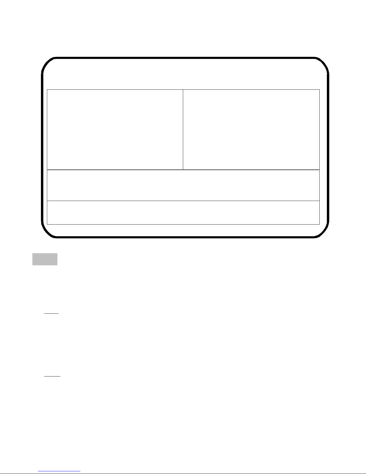
The main menu screen is dis played on the fol low ing page. Each of the op tions will be dis cussed in
this sec tion. Use the ar row keys to high light the de sired se lec tion and press EN TER to en ter the sub menu or to exe cute the func tion se lected.
030923 OPERATIONS MANUAL EBC-BX Page 3 - 1
Page 35
WinSystems - "The Embedded Systems Authority"
Phoenix - AwardBIOS CMOS Setup Utility.
Standard CMOS Features Frequency/Voltage Control
Advanced BIOS FEATURES Load Bios Defaults
Advanced Chipset Features
Integrated Peripherals Set Supervisor Password
Power Management Setup Set User Password
PnP/PCI Configuration Save & Exit Setup
PC Health Status Exit Without Saving
Esc : Quit :Select Item
F10 : Save & Exit Setup
Time, Date. Hard Disk, Type...
↑ ↓ → ←
3.4 Stan dard CMOS Features
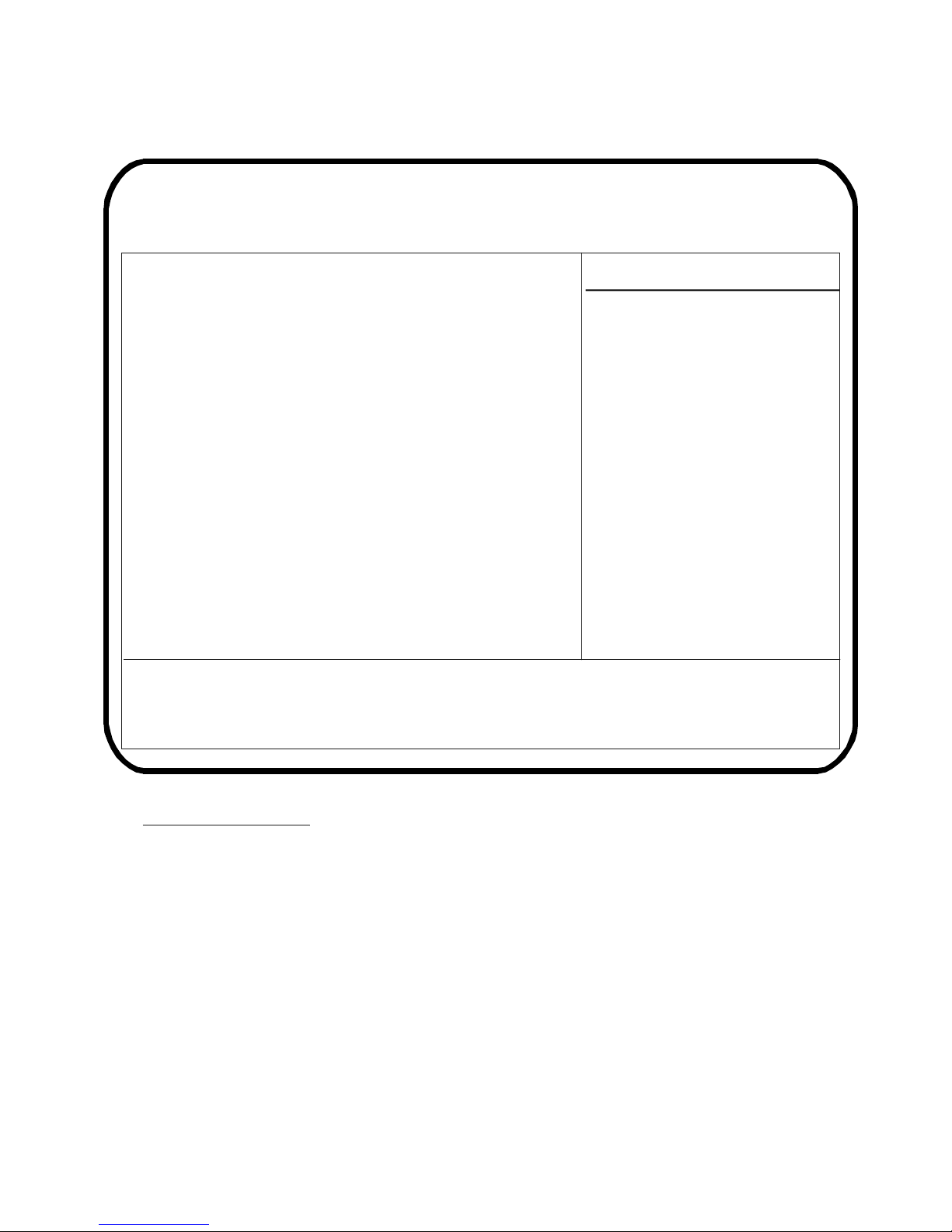
The items in the Stan dard CMOS Setup menu are di vided into sev eral cate go ries. Each cate gory
may in clude one or more setup items. Use the ar row keys to high light the item and then use the PgUp,
PgDn, +.-. keys to se lect the de sired value for the item.
Date
The date for mat is <day>,< date>,< month>, <year>
Day = The day, from Sun to Sat, de ter mined by the BIOS and is dis play only
Date = the date, from 1 to 31 (or the maxi mum for the cur rent month)
Month = the month, JAN through DEC
Year = The year, from 1900 to 2099
Time
The time is hour, minute, sec ond. The time is cal cu lated on the 24- hour, military- time clock such
that 1:00PM is 13:00:00.
Page 3 - 2 OPERATIONS MANUAL EBC-BX 030923
Page 36
WinSystems - "The Embedded Systems Authority"
Phoenix - AwardBIOS CMOS Setup Utility
Standard CMOS Features
Date (mm:dd:yy) Wed Dec 4 2002
Time (hh:mm:ss) 13:57:21
IDE Primary Master [MAXTOR 6L020J1]
IDE Primary Slave [None]
IDE Secondary Master [HL-DT-STDVD-ROM GR8]
IDE Secondary Slave [None]
Drive A [1.44M, 3.5 in.]
Drive B [None]
Video [EGA/VGA]
Halt On [No Errors]
Base Memory 640K
Extended Memory 261120K
Total Memory 262144K
: Move Enter : Select PU/PD/+/- : Value F10 : Save ESC : Exit F1 : General Help
↑ ↓ → ←
F5 : Previous Values F6 : Fail-Safe Defaults F7 : Optimized Defaults
Item Help
Menu Level
Press [Enter] to enter
next page for detail
hard drive settings.
IDE Pri mary Master
Press ing [En ter] brings up a sub- menu screen of choices regarding the Pri mary fixed disk.
IDE HDD Auto-Detection
Press ing [En ter] when this se lec tion is high lighted will cause the sys tem to
in ter ro gate the at tached hard disk and choose the pa rame ters auto mati cally
030923 OPERATIONS MANUAL EBC-BX Page 3 - 3
Page 37

WinSystems - "The Embedded Systems Authority"
IDE Pri mary Mas ter
Press ing [En ter], when this item is high lighted, al lows for se lec tion of how
pa rame ters for the hard drive will be de ter mined. The choices are :
None - No Hard Drive is in stalled
Auto - Auto mati cally de tect the hard disk pa rame ters at power- up
(Rec ommended Set ting)
Man ual - Use the pa rame ters en tered manu ally by the user
Ac cess Mode
Press ing [En ter] when this op tion is high lighted al lows se lec tion of the hard disk
ac cess mode. The choices are :
CHS - The drive will be ac cessed us ing di rect Cyl in der, Head, Sec tor mode.
No transla tion will take place. This can only be used when the “man ual”
mode is se lected above.
LBA - This se lec tion al lows the na tive mode of the drive to be trans lated to
Cyl in der, head, and sec tor counts that are com pati ble with al low able
BIOS pa rame ter re stric tions. Drives up to 120GB can be used with
this mode.
LARGE - This is an other trans la tion scheme that is not com monly used but may
be re quired for some O/Ss.
AUTO - This mode chooses the ap pro pri ate trans la tion mode (usu ally LBA) for
the ac tual drive at tached. (Rec om mended Set ting)
Drive Pa rame ters/Size
The drive size in MB is dis played for all modes. When man ual and CHS modes are
se lected the user may en ter val ues into these fields :
Cyl in der - 0 to 65535
Head - 0 to 255
Pre comp - 0 to 65535
Land ing Zone - 0 to 65535
Sec tor - 0 to 255
IDE Pri mary Slave
This se lec tion is iden ti cal to the IDE Pri mary Mas ter shown above.
IDE Sec on dary Mas ter
This se lec tion is iden ti cal to the IDE Pri mary Mas ter shown above.
IDE Sec on dary Slave
This se lec tion is iden ti cal to the IDE Pri mary Mas ter shown above.
Page 3 - 4 OPERATIONS MANUAL EBC-BX 030923
Page 38

WinSystems - "The Embedded Systems Authority"
Drive A type/Drive B type
This cate gory iden ti fies the type of floppy drives at tached as Drive A: or Drive B:.
The choices are as fol lows :
NONE
360K, 5.25 in.
1.2M, 5.25 in.
720K, 3.5 in
1.44M, 3.5 in.
2.88M 3.5 in.
Video
This cate gory speci fies the type of video adapter used for the pri mary sys tem moni tor that matches
your video dis play board and moni tor. The avail able choices are:
EGA/VGA
CGA40
CGA80
MONO
The EBC-BX has built- in VGA sup port so EGA/VGA should be se lected.
Er ror Halt
This cate gory de ter mines whether the sys tem will halt if a non fa tal er ror is de tected dur i ng
the power-up self test. The choices are:
No Er rors : The sys tem will not be stopped for any er ror that may be de tected.
All Er rors : When ever the BIOS de tects a non fa tal er ror, the sys tem will be
stopped and a prompt will ap pear.
All, but Key board : The sys tem will not stop for a key board er ror, it will stop for all
other er rors.
All, but disk ette : The sys tem will not stop for disk er rors. All oth ers will re sult in a
prompt.
All but Disk/Key : All er rors ex cept disk ette or key board will re sult in a halt and a
prompt.
030923 OPERATIONS MANUAL EBC-BX Page 3 - 5
Page 39

WinSystems - "The Embedded Systems Authority"
Mem ory
This cate gory is dis play only and is de ter mined by the BIOS POST (Power-On Self Test).
Base Mem ory
The POST rou tines in the BIOS will de ter mine the amount of base (con ven tional) mem ory in stalled
in the sys tem. The value of the base mem ory is typi cally 640K for sys tems with a Mega byte of mem ory
or greater.
Ex tended Mem ory
The BIOS de ter mines how much ex tended mem ory is pres ent dur ing the POST. This is the amount
of mem ory lo cated above 1MB in the CPU's mem ory ad dress space.
Total Mem ory
The BIOS dis plays the to tal of the Base mem ory and the Ex tended mem ory in stalled in the sys t em.
.
3.5 Advanced BIOS Fea tures Setup
Vi rus Warn ing
This op tion when en abled, pro tects the boot sec tor and par ti tion ta ble of the hard disk against un au -
thor ized writes through the BIOS. Any at tempt to al ter these ar eas will re sult in an er ror mes sage and a
prompt to author ize the ac tiv ity.
CPU In ter nal Cache
This op tion, when en abled, pro vides maxi mum per form ance by cach ing in struc tions and data us ing
the on- chip cache of the Pentium proc es sor.
Ex ter nal Cache
This op tion, when en abled, fur ther en hances per form ance by cach ing re cently used in struc tions
and data into fast SRAM.
Page 3 - 6 OPERATIONS MANUAL EBC-BX 030923
Page 40
WinSystems - "The Embedded Systems Authority"
Phoenix - AwardBIOS CMOS Setup Utility
Advanced BIOS Features
Virus Warning [Disabled]
CPU Internal Cache [Enabled]
External Cache [Enabled]
CPU L2 Cache ECC Checking [Enabled]
Processor Number Feature [Disabled]
Quick Power On Self Test [Enabled]
First Boot Device [Floppy]
Second Boot Device [HDD-0]
Third Boot Device [CD-ROM]
Boot Other Device [Enabled]
Swap Floppy Drives [Disabled]
Boot Up Floppy Seek [Disabled]
Boot Up Numlock Status [On]
Gate A20 Options [Fast]
Typematic Rate Setting [Enabled]
Typematic Rate (Chars/Sec) [6]
Typematic Delay (Msec) [250]
Security Option [Setup]
OS Select for DRAM > 64MB [Non-OS2]
Report No FDD for WIN 95 [No]
Video BIOS Shadow [Enabled]
C8000-CBFFF Shadow [Disabled]
CC000-CFFFF Shadow [Disabled]
D0000-D3FFF Shadow [Disabled]
D4000-D7FFF Shadow [Disabled]
D8000-DBFFF Shadow [Disabled]
DC000-DFFFF Shadow [Disabled]
Small Logo (EPA) Show [Disabled]
Item Help
Menu Level
Allows you to choose the
VIRUS warning feature for IDE
hard disk boot sector protection. If
this function is enabled and
someone attempt to write data
into this area , BIOS will show a
warning message on screen and
alarm beep
↑ ↓ → ←
: Move Enter : Select PU/PD/+/- : Value F10 : Save ESC : Exit F1 : General Help
F5 : Previous Values F6 : Fail-Safe Defaults F7 : Optimized Defaults
CPU L2 Cache ECC Checking
This op tion when en able pro vides ECC va lid ity check ing to the L2 cache reads.
030923 OPERATIONS MANUAL EBC-BX Page 3 - 7
Page 41

WinSystems - "The Embedded Systems Authority"
Proc es sor Num ber Fea ture
This fea ture when en abled al lows soft ware to read the unique Proc es sor Se rial number pres ent on
the In tel proc es sors.
Quick Power On Self Test (POST)
This op tion, when en abled, speeds up the POST dur ing power up. The BIOS will shorten and/or
skip some items dur ing POST.
First Boot De vice
This op tions al lows for se lec tion of the pri mary or “First” boot de vice. The BIOS will at tempt to
boot from this de vice first. The menu se lec tion are :
Floppy
LS120
HDD-0
SCSI
CD- ROM
HDD-1
HDD-2
HDD-3
ZIP100
LAN
Dis abled
Note : Not all of these de vices will be avail able and se lec tion of a non ex ist ent de vice may re sult in a
dras tic in crease in boot time.
Sec ond Boot De vice
This op tion al lows for se lec tion of the sec on dary choice for boot me dia us age. The op tions are iden -
ti cal to those given above for the “First Boot De vice”.
Third Boot De vice
This op tion al lows for se lec tion of a third choice of boot me dia. The op tions are the same as for the
pre vious two menu items.
Boot Other De vice
The op tion when en abled al lows other de vices with self- contained boot firmware to be come the pri -
mary boot me dia.
Page 3 - 8 OPERATIONS MANUAL EBC-BX 030923
Page 42

WinSystems - "The Embedded Systems Authority"
Swap Floppy Drive
This op tion al lows for swap ping of the A: and B: floppy drives with out ac tu ally re lo cat ing the
drives on the ca ble.
Boot Up Floppy Seek
Dur ing POST, when this op tion is en abled, the BIOS will de ter mine if the floppy drive is 40 track or
80 tracks. If dis abled, no seek test will be per formed and no er ror can be re ported.
Boot Up Num lock Status
This al lows user se lec tion of the Num lock state at boot time.
Gate A20 Op tion
This op tion al lows for the se lec tion of the source for the gate A20 sig nal. The choices are:
Nor mal - Sour ced from the key board con trol ler
Fast - Sour ced from the Chipset
Type matic Rate Set ting
This op tion en ables or dis ables the type matic rate pro gram ming at boot time. Type matic is the auto repeat func tion for the key board.
Type matic Rate
When the type matic rate set ting is en abled, the type matic re peat speed is set via this op tion. The
sup ported rates are :
6 char ac ters per sec ond
8 char ac ters per sec ond
10 char ac ters per sec ond
12 char ac ters per sec ond
15 char ac ters per sec ond
20 char ac ters per sec ond
24 char ac ters per sec ond
30 char ac ters per sec ond
030923 OPERATIONS MANUAL EBC-BX Page 3 - 9
Page 43

WinSystems - "The Embedded Systems Authority"
Type matic De lay
When type matic rate set ting is en abled, this op tion speci fies the time in mil li sec onds bef ore auto-
repeat be gins. The sup ported val ues are:
250 mS
500 mS
750 mS
1000 mS
Se cu rity Op tion
This op tion al lows you to limit ac cess to the sys tem and setup, or just to setup. The choices are:
Sys tem - The sys tem will not boot and ac cess will be de nied if the cor rect pass word is not en tered
at the prompt.
Setup - The sys tem will boot, but ac cess to Setup will be de nied if the cor rect pass word is not en tered
at the prompt.
NOTE: To dis able se cu rity, se lect “Pass word Set ting” at the Setup Main Menu and then you will be
asked to en ter a pass word. Do not type any thing, just hit EN TER. Once the se cu rity is dis abled, the sys tem will boot and you can en ter Setup freely.
OS Select for DRAM > 64MB
This option allows selection of an operating system for DRAM greater than 64MB.
The options are:
OS2
Non- OS2
Report No FDD for Win 95
This option, when enabled, signals Windows 95 if there is no floppy present.
The options are:
Yes
No
Page 3 - 10 OPERATIONS MANUAL EBC-BX 030923
Page 44

WinSystems - "The Embedded Systems Authority"
Shad ow ing Op tions
When shad ow ing for a par ticu lar ad dress range is en abled, it in structs the BIOS to copy the BIOS
lo cated in ROM into DRAM. This shad ow ing from an 8- bit EPROM into fast 32- bit DRAM re sults in a
Multi- magnitude in crease in per form ance. The main BIOS is shad owed auto mati cally but there are
other ar eas that may be se lected for shad ow ing as shown here:
Video BIOS Shadow - C000- C7FFF EGA/VGA BIOS ROM
C8000- CBFFF
CC000- CFFFF
D0000- D3FFF
D4000- D7FFF
D8000- DBFFF
DC000- DFFFF
Small Logo(EPA) Show
This op tion when en abled in structs the BIOS to dis play the EPA Energy- Star logo in the up per right
cor ner of the screen dur ing the POST pro cess.
3.6 Chipset Fea tures Setup
The op tions in this sec tion con trol the chipset pro gram ming at boot time. In most cases, the de fault
set tings should be used un less you have a clear un der stand ing of the sig nifi cance of the change. It is pos si ble us ing these op tions to cre ate a sys tem that will ei ther not boot or is very un sta ble or un re li able. If
this should oc cur, there are two meth ods to re turn the sys tem to a sta ble con figu ra tion. If the sys tem
works well enough to get into Setup, sim ply choose the “Load BIOS De faults” op tion and then se l ect
“Save and Exit Setup” to re store fac tory de faults. If the sys tem will not run well enough to run Setup, it
will be nec es sary to re move the bat tery source tem po rar ily un til the CMOS mem ory de cays. Ref er to
Sec tion 2.7 for de tails on re ini tial iz ing the CMOS RAM.
Each of the op tions for the Chipset Fea tures Menu will be briefly dis cussed in the sections that fol low.
SDRAM RAS- to- CAS De lay
This op tion al lows for se lec tion of the number of clock to de lay the RAS to CAS tran si tion. The
avail able choices are :
3 Clocks
2 Clocks
030923 OPERATIONS MANUAL EBC-BX Page 3 - 11
Page 45

WinSystems - "The Embedded Systems Authority"
Phoenix - AwardBIOS CMOS Setup Utility
Advanced Chipset Features
SDRAM RAS-to-CAS Delay [3]
SDRAM RAS Precharge Time [3]
SDRAM CAS Latency Time [3]
SDRAM Precharge Control [Enabled]
DRAM Data Integrity Mode [Non-ECC]
System BIOS Cacheable [Disabled]
Video BIOS Cacheable [Disabled]
Video RAM Cacheable [Disabled]
8 Bit I/O Recovery Time [1]
16 Bit I/O Recovery Time [1]
Memory Hole at 15M-16M [Disabled]
AGP Aperture Size (MB) [64]
↑ ↓ → ←
: Move Enter : Select PU/PD/+/- : Value F10 : Save ESC : Exit F1 : General Help
F5 : Previous Values F6 : Fail-Safe Defaults F7 : Optimized Defaults
Item Help
Menu Level
SDRAM RAS Pre charge Time
This op tions al lows for set ting the SDRAM RAS pre charge tim ing. The choices are :
3 clocks
2 clocks
SDRAM CAS La tency Time
This op tion al lows con trol of the SDRAM CAS la tency tim ing. The choices are :
3 clocks
2 clocks
Page 3 - 12 OPERATIONS MANUAL EBC-BX 030923
Page 46

WinSystems - "The Embedded Systems Authority"
SDRAM Pre charge Con trol
This op tion, when en abled, al low con trol of the SDRAM pre charge tim ing.
Sys tem BIOS Cache able
This op tion enables or disables cacheability of the system BIOS.
Video BIOS Cacheable
This op tion enables or disables cacheability of the video BIOS.
8 Bit I/O Recovery
Enables and defines 8-bit I/O recovery time in number of clocks.
16 Bit I/O Recovery
Enables and defines 16-bit I/O recovery time in number of clocks.
Memory Hole At 15M-16M
This option, when enabled, disables onboard memory be tween 15M and 16M.
AGP Ap er ture Size (MB)
This op tion speci fies the amount of ad dress space to al lo cate to the AGP video ap er ture. The
choices are :
4
8
16
32
64
128
256
030923 OPERATIONS MANUAL EBC-BX Page 3 - 13
Page 47
WinSystems - "The Embedded Systems Authority"
3.7 In te grated Pe riph er als Setup
The op tions in this sec tion al low for con trol of the in te grated pe riph er als, i.e. Floppy and IDE con -
trol lers, se rial ports, and the par al lel port.
Phoenix - Award BIOS CMOS Setup Utility
Integrated Peripherals
IDE 1st Channel Cable [40 Pins]
IDE 2nd Channel Cable [40 Pins]
IDE Primary Master PIO [Auto]
IDE Primary Slave PIO [Auto]
IDE Secondary Master PIO [Auto]
IDE Secondary Slave PIO [Auto]
IDE Primary Master UDMA [Auto]
IDE Primary Slave UDMA [Auto]
IDE Secondary Master UDMA [Auto]
IDE Secondary Slave UDMA [Auto]
On-Chip Primary PCI IDE [Enabled]
On-Chip Secondary PCI IDE [Enabled]
USB Keyboard Support [Disabled]
Init Display First [AGP]
IDE HDD Block Mode [Enabled]
Onboard FDC Controller [Enabled]
Onboard Serial Port 1 [3F8/IRQ4]
Onboard Serial Port 2 [2F8/IRQ3]
Onboard Parallel Port [378/IRQ7]
Parallel Port Mode [ECP+EPP1.9]
ECP Mode Use DMA [3]
Item Help
Menu Level
↑ ↓ → ← : Move Enter : Select PU/PD/+/- : Value F10 : Save ESC : Exit F1 : General Help
F5 : Previous Values F6 : Fail-Safe Defaults F7 : Optimized Defaults
IDE 1st Chan nel Ca ble
This op tion al lows for speci fi ca tion of the ca ble type at tached to the Pri mary IDE chan nel. The
choices are :
40 Pins
80 Pins
Page 3 - 14 OPERATIONS MANUAL EBC-BX 030923
Page 48

WinSystems - "The Embedded Systems Authority"
IDE 2nd Chan nel Ca ble
This op tion al lows the ca ble type to be speci fied for the sec on dary IDE chan nel. The choices are :
40 Pins
80 Pins
IDE Pri mary Mas ter PIO
This op tion al lows se lec tion of the PIO mode to be used with the Pri mary Mas ter IDE de vice. The
choices are :
Auto
Mode 0
Mode 1
Mode 2
Mode 3
Mode 4
IDE Pri mary Slave PIO
This op tion al lows for se lec tion of the PIO mode to be used with a Pri mary Slave IDE de vice. The
choices are :
Auto
Mode 0
Mode 1
Mode 2
Mode 3
Mode 4
IDE Secondary Mas ter PIO
This op tion al lows se lec tion of the PIO mode to be used with the Secondary Mas ter IDE de vice. The
choices are :
Auto
Mode 0
Mode 1
Mode 2
Mode 3
Mode 4
030923 OPERATIONS MANUAL EBC-BX Page 3 - 15
Page 49

WinSystems - "The Embedded Systems Authority"
IDE Secondary Slave PIO
This op tion al lows for se lec tion of the PIO mode to be used with a Secondary Slave IDE de vice.
The choices are :
Auto
Mode 0
Mode 1
Mode 2
Mode 3
Mode 4
IDE Pri mary Mas ter UDMA
This op tion al lows for se lect ing whether an UDMA mode will be used for disk trans fers on the Pri -
mary Mas ter IDE de vice. The choices are :
Dis abled
Auto
IDE Pri mary Slave UDMA
This op tion al lows for se lect ing whether an UDMA mode will be used for disk trans fers on the Pri -
mary Slave IDE de vice. The choices are :
Dis abled
Auto
IDE Secondary Mas ter UDMA
This op tion al lows for se lect ing whether an UDMA mode will be used for disk trans fers on the
Secondary Mas ter IDE de vice. The choices are :
Dis abled
Auto
IDE Sec on dary Slave UDMA
This op tion al lows for se lect ing whether an UDMA mode will be used for disk trans fers on the Sec -
on dary Slave IDE de vice. The choices are :
Dis abled
Auto
Page 3 - 16 OPERATIONS MANUAL EBC-BX 030923
Page 50

WinSystems - "The Embedded Systems Authority"
On- Chip Pri mary PCI IDE
This op tion en ables or dis ables the on board Pri mary IDE con trol ler.
On- Chip Sec on dary PCI IDE
This op tion en ables or dis ables the on board Sec on dary IDE con trol ler.
USB Key board Sup port
This op tion en ables or dis ables BIOS sup port for USB key boards.
Init Dis play First
This op tion al lows se lec tion of the source for the first, or pri mary, video con trol ler. The choices are :
PCI Slot
AGP
Note : The on board video is im ple mented on the AGP bus. An al ter nate pri mary video dis play may
be used by in stall ing a PC/104Plus video card and set ting this op tion to PCI Slot.
IDE Block Mode
This op tion al lows ena bling of the IDE block mode for disk trans fers.
On board FDC Con trol ler
This op tion con trols the on board Floppy Disk con trol ler. The op tions are :
En abled
Dis abled
On board Se rial Port 1
This op tion al lows for con trol of the first on board se rial port. The op tions are :
Dis abled
3F8/IRQ4
2F8/IRQ3
3E8/IRQ4
2E8/IRQ3
Auto
030923 OPERATIONS MANUAL EBC-BX Page 3 - 17
Page 51

WinSystems - "The Embedded Systems Authority"
On board Se rial Port 2
This op tion al lows for con trol of the sec ond on board se rial port. The op tions are :
Dis abled
3F8/IRQ4
2F8/IRQ3
3E8/IRQ4
2E8/IRQ3
Auto
On board Par al lel Port
This op tion al lows for con figu ra tion of the on board par al lel printer port. The op tions are :
Dis abled
3BC/IRQ7
378/IRQ7
278/IRQ5
Par al lel Port Mode
This op tion con trols the op er at ing mode of the on board par al lel port. The op tions are :
SPP
EPP1.9+SPP
ECP
ECP+EPP1.9
Nor mal
EPP1.7+SPP
ECP+EPP1.7
ECP Mode Use DMA
This op tion con trols which DMA chan nel will be used for ECP trans fers. The choices are:
3
1
Page 3 - 18 OPERATIONS MANUAL EBC-BX 030923
Page 52

WinSystems - "The Embedded Systems Authority"
3.8 Power Man age ment Setup
The items in this menu con trol op era tion of the BIOS based power man age ment func tions.
ACPI func tion
This op tion al lows for con trol of the BIOS level ACPI func tion al ity.
Phoenix - Award BIOS CMOS Setup Utility
Power Management Setup
ACPI Function [Enabled]
Power Management [User Define]
PM Control by APM [Yes]
Video Off Method [V/H SYNC + Blank]
Video Off After [Standby]
Modem Use IRQ [3]
Doze Mode [Disabled]
Standby Mode [Disabled]
Suspend Mode [Disabled]
HDD Power Down [Disabled]
VGA Active Monitor [Disabled]
IRQ 8 Break Suspend [Disabled]
USB Keyboard Support [Disabled]
** Reload Global Timer Events **
IRQ[3-7, 9-15],NMI [Disabled]
Primary IDE 0 [Disabled]
Primary IDE 1 [Disabled]
Secondary IDE 0 [Disabled]
Secondary IDE 1 [Disabled]
Floppy Disk [Disabled]
Serial Port [Disabled]
Parallel Port [Disabled]
Item Help
Menu Level
↑ ↓ → ←
: Move Enter : Select PU/PD/+/- : Value F10 : Save ESC : Exit F1 : General Help
F5 : Previous Values F6 : Fail-Safe Defaults F7 : Optimized Defaults
030923 OPERATIONS MANUAL EBC-BX Page 3 - 19
Page 53

WinSystems - "The Embedded Systems Authority"
Power Man age ment
This op tion al lows for the speci fi ca tion for the type and ex tent of power man age ment op tions. The
choices are :
User De fine
Min Sav ing
Max Sav ing
PM Con trol by APM
This op tion, when en abled, al lows an APM aware OS to con trol sys tem power man age ment. The
op tions are :
Yes
No
Video Off Method
This op tion speci fies the method used for Video blank ing or PM shut down. The op tions are :
Blank Screen
V/H SYNC + Blank
DPMS
Video Off Af ter
This op tion speci fies at what power- management stage the video off func tion will be exe cuted. The
op tions are :
NA
Sus pend
Standby
Doze
Page 3 - 20 OPERATIONS MANUAL EBC-BX 030923
Page 54

WinSystems - "The Embedded Systems Authority"
Mo dem Use IRQ
This op tion al lows speci fi ca tion of the IRQ used by the mo dem for PM con trol func tions. The op tions are :
NA
3
4
5
7
9
10
11
Doze Mode
This op tion al lows for set ting the time- out value bef ore en ter ing Doze mode or for dis abling Doze
mode com pletely. The op tions are :
Dis able
1 Min
2 Min
4 Min
8 Min
12 Min
20 Min
30 Min
40 Min
1 Hour
Standby Mode
This op tion al lows for set ting the time- out value bef ore en ter ing Standby mode or for dis abling
Standby mode com pletely. The op tions are :
Dis able
1 Min
2 Min
4 Min
8 Min
12 Min
20 Min
30 Min
40 Min
1 Hour
030923 OPERATIONS MANUAL EBC-BX Page 3 - 21
Page 55

WinSystems - "The Embedded Systems Authority"
Suspend Mode
This op tion al lows for set ting the time- out value bef ore en ter ing Sus pend mode or for dis a bling
Sus pend mode com pletely. The op tions are :
Dis able
1 Min
2 Min
4 Min
8 Min
12 Min
20 Min
30 Min
40 Min
1 Hour
HDD Power Down
This op tion al lows se lec tion of a Hard disk power down timer. The op tions are :
Dis able
1 Min
2 Min
3 Min
4 Min
5 Min
6 Min
7 Min
8 Min
9 Min
10 Min
11 Min
12 Min
13 Min
14 Min
15 Min
VGA Ac tive Moni tor
This op tion when en abled tracks video changes for PM ac tiv ity status.
IRQ 8 Break Sus pend
This op tion when en abled al lows an RTC alarm event to awaken from a sus pend event.
Page 3 - 22 OPERATIONS MANUAL EBC-BX 030923
Page 56
WinSystems - "The Embedded Systems Authority"
Re load Global Timer Events
The 8 op tions that fol low al low in di vid ual se lec tion of IRQs or de vices to moni tor. Ac tiv ity on any
of the en abled op tions re sets the count down tim ers de lay ing any fur ther power man age ment steps.
The items that can be en abled for moni tor ing are :
IRQ[3-7, 9-15], NMI
Pri mary IDE 0
Pri mary IDE 1
Sec on dary IDE 0
Sec on dary IDE 1
Floppy Disk
Se rial Port
Par al lel Port
3.9 PNP/PCI Con figu ra tion
The op tions in this sec tion con trol PNP and PCI re sources.
Phoenix - AwardBIOS CMOS Setup Utility
PNP/PCI Configuration
PNP OS Installed [No]
Reset Configuration Data [Disabled]
Resources Controlled by [Manual]
IRQ Resources [Press Enter]
DMA Resources [Press Enter]
Memory Resources [Press Enter]
PCI/VGA Palette Snoop [Disabled]
↑ ↓ → ← : Move Enter : Select PU/PD/+/- : Value F10 : Save ESC : Exit F1 : General Help
F5 : Previous Values F6 : Fail-Safe Defaults F7 : Optimized Defaults
Item Help
Menu Level
Select yes if you are using a Plug
and Play capable operating
system. Select No if you need the
BIOS to configure non-boot
devices
030923 OPERATIONS MANUAL EBC-BX Page 3 - 23
Page 57

WinSystems - "The Embedded Systems Authority"
PNP OS In stalled
This op tion al lows the user to as sign whether the op er at ing sys tem is Plug and Play compatible. The
op tions are:
Yes
No
Re set Con figu ra tion Data
This op tion, when en abled, will re set the con figu ra tion data on power up. The op tions are:
En abled
Disabled
Re sources Con trolled By
This op tion al lows the user to se lect re source con trol of the sys tem. The op tions are:
Auto (ESCD)
Manual
IRQ Re sources
This op tion al lows for IRQs to be re served for Leg acy ISA de vices or to be used in the pool of avail -
able IRQs for PCI and ISA PnP de vices.
DMA Re sources
This op tion al lows for DMA re sources to be re served for leg acy ISA de vices or to be used in the
pool of avail able DMA re sources for PCI or ISA PnP de vices.
Mem ory Re sources
This op tion al lows for re serv ing an up per mem ory block with a size be tween 8K and 64K Bytes.
The avail able start ing seg ment ad dresses for this re served block are :
C800
CC00
D000
D400
D800
DC00
Page 3 - 24 OPERATIONS MANUAL EBC-BX 030923
Page 58
WinSystems - "The Embedded Systems Authority"
PCI/VGA Pal ette Snoop
This op tion when en abled per mits PCI/VGA pal ette snoop ing.
3.10 PC Health Status
This op tion is dif fer ent from the other setup menu items in that there are no con fig ur able op tions.
This is sim ply a status screen that can be used to ex am ine the status of vari ous tem pera tures and volt ages on the board.
Phoenix - AwardBIOS CMOS Setup Utility
PC Health Status
Current Systems Temp 30°C / 86°F
Current CPU Temp 39°C / 102°F
Current CPUFAN1 Speed 3740 RPM
Current CPUFAN2 Speed 0 RPM
+2.5 Volts 2.51 V
Vcore 1.36 V
+3.3 Volts 3.36 V
+5.0 Volts 4.97 V
+12.0 Volts 11.97 V
VCCT 1.48 V
↑ ↓ → ←
: Move Enter : Select PU/PD/+/- : Value F10 : Save ESC : Exit F1 : General Help
F5 : Previous Values F6 : Fail-Safe Defaults F7 : Optimized Defaults
Item Help
Menu Level
3.11 Fre quency/Volt age Con trol
The items in this menu al low for con figu ra tion of cer tain clock con trol items.
Auto De tect PCI/DIMM Clk
This op tion when en abled, in structs the BIOS to turn off un used clocks to DIMM sock ets and PCI
slots.
030923 OPERATIONS MANUAL EBC-BX Page 3 - 25
Page 59
WinSystems - "The Embedded Systems Authority"
Phoenix - AwardBIOS CMOS Setup Utility
Frequency/Voltage Control
Auto Select PCI/DIMM Clk [Enabled]
Spread Spectrum [Disabled]
↑ ↓ → ←
: Move Enter : Select PU/PD/+/- : Value F10 : Save ESC : Exit F1 : General Help
F5 : Previous Values F6 : Fail-Safe Defaults F7 : Optimized Defaults
Item Help
Menu Level
Spread Spec trum
This op tion en ables the pur pose ful jit ter ing of all of the pri mary Clock fre quen cies by the per cent -
ages given by the choices shown here.
Dis abled
-0.5%
+/-0.5%
+/-0.25%
3.12 Load BIOS De faults
This op tion when se lected, re loads all of the CMOS set tings with the fac tory specified set tings.
Page 3 - 26 OPERATIONS MANUAL EBC-BX 030923
Page 60

WinSystems - "The Embedded Systems Authority"
3.13 Set Su per vi sor Pass word
This op tion, when a pass word has been en tered, pro tects the Setup menus from un au thor ized al tera tion of the op tions. Hit ting “En ter” when prompted for the pass word, dis ables the pass word se cu rity.
3.14 Set User Pass word
This op tion pro vides a sec ond level of pass word se cu rity to the BIOS setup screens. When both the
Su per vi sor and the User pass words are en abled. The user will only be able to al ter fixed disk info. If no
Su per vi sor pass word is en abled, the user ac cess pass word al lows full ac cess to the Setup screens. The
sec urity op tion is dis abled by hit ting “En ter” at the pass word prompt.
3.15 Save & Exit Setup
This func tion writes all changes to CMOS RAM and re starts the sys tem.
3.16 Exit with out Sav ing
This op tion ex its setup with out sav ing any changes made and then re starts the sys tem.
030923 OPERATIONS MANUAL EBC-BX Page 3 - 27
Page 61

4 EBC-BX Disk On Chip Con figu ra tion
4.1 Disk On Chip Us age
The EBC- BX sup ports the M- Systems’ DiskOnChip (DOC) flash de vice in sizes rang ing from
8MB to over 500MB. The DOC de vice con tains a BIOS ex ten sion, the TFFS (True Flash File Sys tem),
and the Flash mem ory all in a sin gle 32- pin de vice. The DOC emu lates a hard disk and can be used as a
sec on dary hard disk to a physi cal IDE drive or it can be the only hard disk in the sys tem.
The DOC is in stalled into the socket at U15. Ref er to the sec tion 2.19 for cor rect de vice jump er ing
and ena bling of the DOC.
4.2 DOC Ini tiali za tion
The DOC is ini tial ized in an iden ti cal fash ion to a fixed disk. DOS is booted (from floppy or hard
disk), FDISK is run on the DOC drive (be sure to get the right drive), the sys tem is re booted and then the
DOC is for mat ted us ing the DOS for mat com mand.
If the /S switch was used dur ing for mat ting and there is no other fixed disk de vice speci fied or at tached to the sys tem the DOC will be come the boot de vice. If a hard disk is pres ent, the DOC will be come a sec on dary fixed disk.
030923 OPERATIONS MANUAL EBC-BX Page 4 - 1
Page 62

5 WS16C48 Pro gram ming Ref er ence
5.1 In tro duc tion
This sec tion pro vides ba sic docu men ta tion for the in cluded I/O rou tines. It is in tended that the ac com pa ny ing source code equip the pro gram mer with a ba sic li brary of I/O func tions for the WS16C48
or can serve as the ba sis from which ap pli ca tion spe cific code can be de rived.
5.2 Func tion Defi ni tions
This sec tion briefly de scribes each of the func tions con tained in the driver. Where nec es sary, short
ex am ples will be pro vided to il lus trate us age. Any ap pli ca tion mak ing use of any of the driver func tions
should in clude the header file “uio48.h”, which in cludes the func tion pro to types and the needed con stant defi ni tions.
Note that all of the func tions util ize the con cept of “bit_number”. The “bit_number” is a value from
1 to 48 (1 to 24 for in ter rupt re lated func tions) that cor re lates to a spe cific I/O pin. Bit_number 1 is port
0 bit 0 and con tin ues through to bit_number 48 at port 5 bit 7.
INIT_IO - Ini tial ize I/O, set all ports to in put
Syn tax
void init_io(un signed io_ad dress);
De scrip tion
This func tion takes a sin gle ar gu ment:
io_ad dress - The I/O ad dress of the WS16C48 chip.
There is no re turn value. This func tion ini tial izes all I/O pins for in put (sets them high), dis ables all
in ter rupt set tings, and sets the im age val ues.
030923 OPERATIONS MANUAL EBC-BX Page 5 - 1
Page 63

WinSystems - "The Embedded Systems Authority"
READ_BIT - Reads an I/O port Bit
Syn tax
int read_bit(int bit_number);
De scrip tion
This func tion takes a sin gle ar gu ment:
bit_number - This is a value from 1 to 48 that in di cates the I/O pin to read from.
This func tion re turns the state of the I/O pin. A '1' is re turned if the I/O pin is low and a '0' is re turned
if the pin is high.
WRITE_BIT - Write a 1 or 0 to an I/O pin
Syn tax
void write_bit(int bit_number, int value);
De scrip tion
This func tion takes two ar gu ments:
bit_number - This is value from 1 to 48, which is the bit to be acted upon.
Value - is ei ther 1 or 0.
This func tion al lows for writ ing of a sin gle bit to ei ther a '0' or a '1' as speci fied by the sec ond ar gu -
ment. There is no re turn value and other bits in the I/O port are not af fected.
Page 5 - 2 OPERATIONS MANUAL EBC-BX 030923
Page 64

WinSystems - "The Embedded Systems Authority"
SET_BIT - Set the speci fied I/O Bit
Syn tax
void set_bit(int bit_number);
De scrip tion
This func tion takes a sin gle ar gu ment:
bit_number - a value be tween 1 and 48 speci fy ing the port bit to be set.
This func tion sets the speci fied I/O port bit. Note that set ting a bit re sults in the I/O pin ac tu ally go ing low. There is no re turn value and other bits in the same I/O port are un af fected.
CLR_BIT - Clear the speci fied I/O Bit
Syn tax
void clr_bit(int bit_number);
De scrip tion
This func tion takes a sin gle ar gu ment:
bit_number - a value from 1 to 48 in di cates the bit number to clear.
This func tion clears the speci fied I/O bit. Note that clear ing the I/O bit re sults in the ac tual I/O pin
go ing high. This func tion does not af fect any bits other than the one speci fied.
030923 OPERATIONS MANUAL EBC-BX Page 5 - 3
Page 65

WinSystems - "The Embedded Systems Authority"
ENAB_INT - En able Edge In ter rupt, Se lect Po lar ity
Syn tax
void enab_int(int bit_number, int po lar ity);
De scrip tion
This func tion re quires two ar gu ments:
bit_number - A value from 1 to 24 speci fy ing the ap pro pri ate bit
po lar ity - Speci fies ris ing or fal ling edge po lar ity de tect. The con stants RIS ING and FAL LING are de fined
in “uio48.h”
This func tion en ables the edge de tec tion cir cuitry for the speci fied bit at the speci fied po lar ity. It
does not un mask the in ter rupt con trol ler, in stall vec tors, or han dle in ter rupts when they oc cur. There is
no re turn value and only the speci fied bit is af fected.
DISAB_INT - Dis able Edge De tect In ter rupt De tec tion
Syn tax
void disab_int(int bit_number);
De scrip tion
This func tion re quires a sin gle ar gu ment:
bit_number - A value from 1 to 24 speci fy ing the ap pro pri ate bit.
This func tion shuts down the edge de tec tion in ter rupts for the speci fied bit. There is no re turn value
and no harm is done by call ing this func tion for a bit which did not have edge de tec tion in ter rupts en abled. There is no af fect on any other bits.
Page 5 - 4 OPERATIONS MANUAL EBC-BX 030923
Page 66

WinSystems - "The Embedded Systems Authority"
CLR_INT - Clear the speci fied pend ing in ter rupt
Syn tax
void clr_int(int bit_number);
De scrip tion
This func tion re quires a sin gle ar gu ment:
bit_number - The speci fied bit number from 1 to 24 to re set the in ter rupt.
This func tion clears a pend ing in ter rupt on the speci fied bit. It does this by dis abling and reena bling
the in ter rupt. The net re sult af ter the call is that the in ter rupt is no longer pend ing and is re armed for the
next tran si tion of the same po lar ity. Call ing this func tion on a bit that has not been en abled for in ter rupts
will re sult in its in ter rupt be ing en abled with an un de fined po lar ity. Call ing this func tion with no in ter rupt pend ing will have no ad verse af fect. Only the speci fied bit is af fected.
GET_INT - Re trieve bit number of pend ing in ter rupt
Syn tax
int get_int(void);
De scrip tion
This func tion re quires no ar gu ments and re turns ei ther a '0' for no bit in ter rupts pend ing or a value
be tween 1 and 24 rep re sent ing a bit number that has a pend ing edge de tect in ter rupt. The func tion re turns with the first in ter rupt found and be gins its search at Port 0 Bit 0 pro ceed ing through to Port 2 Bit
7. It is nec es sary to use ei ther clr_int() or disab_int() to avoid re turn ing the same bit con tinu ously. This
func tion may ei ther be used in an ap pli ca tion's ISR or can be used in the fore ground to poll for bit tran si tions.
030923 OPERATIONS MANUAL EBC-BX Page 5 - 5
Page 67

WinSystems - "The Embedded Systems Authority"
5.3 Sam ple Pro grams
There are three sam ple pro grams in source code form in cluded on the EBC- BX disk ette in the
UIO48 di rec tory. These pro grams are not use ful by them selves but are pro vided to il lus trate the us age
of the I/O func tions pro vided in UIO48C.
FLASH.C
This pro gram was com piled with Bor land C/C++ ver sion 3.1 on the com mand line with:
bcc flash.c uio48.c
This pro gram il lus trates the most ba sic us age of the WS16C48. It uses three func tions from the
driver code. The io_init() func tion is used to ini tial ize the I/O func tions and the set_bit() and clr_bit()
func tions are used to se quence through all 48 bits turn ing each on and then off in turn.
POLL.C
This pro gram was com piled with Bor land C/C++ ver sion 3.1 on the com mand line with:
bcc poll.c uio48.c
This pro gram il lus trates ad di tional fea tures of the WS16C48 and the I/O li brary func tions. It pro -
grams the first 24 bits for in put, arms them for fal ling edge de tec tion, and then polls us ing the li brary
rou tine get_int() to de ter mine if any tran si tions have taken place.
INT.C
This pro gram was com piled with Bor land C/C++ ver sion 3.1 on the com mand line with:
bcc int.c uio48.c
This pro gram is iden ti cal in func tion to the “poll.c” pro gram ex cept that in ter rupts are ac tive and all
up dat ing of the tran si tion coun ters is ac com plished in the back ground dur ing the in ter rupt serv ice rou tine.
Sum mary
The source code for all three pro grams as well as the I/O rou tines are in cluded on the ac com pa ny ing
disk ette. The source code is also pro vided in printed form in AP PEN DIX F. These I/O rou tines along
with the sam ple pro gram should pro vide for a good ba sis on which to build an ap pli ca tion us ing the fea tures of the WS16C48.
Page 5 - 6 OPERATIONS MANUAL EBC-BX 030923
Page 68

6 AP PEN DIX A - I/O Port Map
The fol low ing is a list of PC I/O ports. Ad dresses marked with a '-' are not used on the EBC- BX but
their use should be care fully quali fied so as not to con flict with other I/O boards. I/O ad dresses marked
with a '+' are used on the EBC- BX board and are unique to the Win Sys tems’ de sign. I/O Ad dresses
marked with '**' are gen er ally un used and should be the ba sis for the first choices in I/O ad d ress se lec tion.
Hex Range Us age
000- 00F 8237 DMA #1
**010- 01F FREE
020- 021 8259 PIC #1
+022- 023 Fi nali 486 Chipset Reg is ters
**024- 03F FREE
040- 043 8254 Timer
**044- 05F FREE
060- 06F 8042 Key board Con trol ler
070- 071 CMOS RAM/RTC
**072- 07F FREE
080- 08F DMA Page Reg is ters
**090- 09F FREE
0A0- 0BF 8259 PIC #2
0C0- 0DF 8237 DMA #2
**0E0- 0EF FREE
0F0- 0F1 Co proc es sor Con trol
**0F2- 11F FREE
+120- 12F WS16C48 HDIO
**130- 1DF FREE
+1E0- 1EF SSD, Led, Watch dog con trol
1F0- 1FF Fixed Disk I/O
-200- 20F Joy stick port
-210- 21F PCM SSD I/O Ports
-220- 22F Sound blas ter I/O ports
**230- 237 FREE
-238- 23B BUS Mouse
**240- 277 FREE
278- 27F LPT1
**280- 2AF FREE
-2B0 -2DF EGA Video
-2E0 -2E7 GPIB In ter face
2E8- 2EF COM4
**2F0- 2F7 FREE
2F8- 2FF COM2
-300- 31F Pro to type Card
-320- 32F XT Hard Disk
**330- 377 FREE
-378- 37F Par al lel Printer
-380 -3AF SDLC
030923 OPERATIONS MANUAL EBC-BX Page 6 - 1
Page 69

WinSystems - "The Embedded Systems Authority"
-3B0 -3BB DMA
-3C0 -3CF EGA
3E8- 3EF COM3
3F0- 3F6 Floppy Disk
3F8- 3FF COM1
Page 6 - 2 OPERATIONS MANUAL EBC-BX 030923
Page 70

7 AP PEN DIX B - In ter rupt Map
No. Ad dress Type De scrip tion
0 00 CPU Di vide by 0
1 04 CPU Sin gle Step
386 De bug Ex cep tion
2 08 CPU NMI
3 0C CPU Break point
4 10 CPU Over flow
5 14 BIO Print Screen
186 Bound Ex cep tion
6 18 186 In va lid op code ex cep tion
7 1C 186 Co proc es sor un avail able
8 20 Hard ware IRQ0 - 18.2Hz heart beat
286 LIDT - Dou ble fault ex cep tion
9 24 Hard ware IRQ1 - Key board in ter rupt
286 Co proc es sor seg ment
A 28 Hard ware IRQ2 - XT Re served,
AT-Slaved Con trol ler
286 In va lid TSS ex cep tion
B 2C Hard ware IRQ3 - COM2
286 Seg ment not pres ent
C 30 Hard ware IRQ4 - COM1
286 Stack fault ex cep tion
D 34 Hard ware IRQ5 - XT Hard Disk, AT Free
286 Pro tec tion fault ex cep tion
E 38 Hard ware IRQ6 - Floppy Disk In ter rupt
386 Page fault ex cep tion
F 3C Hard ware IRQ7 - LPT1
10 40 BIOS Video BIOS func tions
286 Co proc es sor ex cep tion
11 44 BIOS BIOS Equip ment check
486 Align ment check ex cep tion
12 48 BIOS Mem ory Size func tion
13 4C BIOS BIOS Disk func tions
14 50 BIOS BIOS se rial func tions
15 54 BIOS Cas sette/pro tected mode
func tions
16 58 BIOS Key board BIOS func tions
17 5C BIOS BIOS printer func tions
18 60 BIOS SROM Ba sic En try point (IBM)
19 64 BIOS Boot loader func tion
1A 68 BIOS BIOS time of day func tions
1B 6C BIOS Key board break vec tor
1C 70 BIOS User chained timer tick
1D 74 BIOS Video Ini tiali za tion
1E 78 BIOS Floppy Disk pa rame ter ta ble
1F 7C BIOS CGA graphic char ac ter font
030923 OPERATIONS MANUAL EBC-BX Page 7 - 1
Page 71

WinSystems - "The Embedded Systems Authority"
20 80 MS- DOS Pro gram ter mi nate
21 84 MS- DOS DOS func tion call
22 88 MS- DOS Ter mi nate Ad dress
23 8C MS- DOS Ctrl- Break Ad dress
24 90 MS- DOS Fa tal Er ror Vec tor
25 94 MS- DOS Ab so lute disk read
26 98 MS- DOS Ab so lute disk write
27 9C MS- DOS Ter mi nate
28 A0 MS- DOS Idle Sig nal
29 A4 MS- DOS TTY out put
2A A8 MS- DOS MS- Net serv ices
2F BC MS- DOS Print Spool
30 C0 MS- DOS Long jump in ter face
33 CC MS- DOS Mouse func tions
3F FC MS- DOS Over lay in ter rupt
40 100 BIOS Floppy I/O when fixed disk
is pres ent
41 104 BIOS Fixed disk 1 pa rame ter ta ble
42 108 BIOS EGA Chain
43 10C BIOS EGA Pa rame ter ta ble pointer
44 110 BIOS EGA graph ics char ac ter font
4A 128 BIOS AT Alarm exit ad dress
50 140 BIOS AT Alarm in ter rupt
51 144 BIOS Mouse func tions
5A 168 NET Func tions
5B 16C NET Boot chain
5C 170 NET Net BIOS en try
67 19C MS- DOS EMS func tions
6D 1B4 VGA VGA Serv ice
70 1C0 Hard ware IRQ8 - Real Time clock
71 1C4 Hard ware IRQ9 - Re di rected IRQ2
72 1C8 Hard ware IRQ10 - Un as signed
73 1CC Hard ware IRQ11 - Un as signed
74 1D0 Hard ware IRQ12 - Un as signed
75 1D4 Hard ware IRQ13 - Un as signed
76 1D8 Hard ware IRQ14 - IDE Fixed Disk
77 1DC Hard ware IRQ15 - Un as signed
80 200
F0 3C0 Ba sic
F1 3C4
FF 3FC Not Used
Page 7 - 2 OPERATIONS MANUAL EBC-BX 030923
Page 72
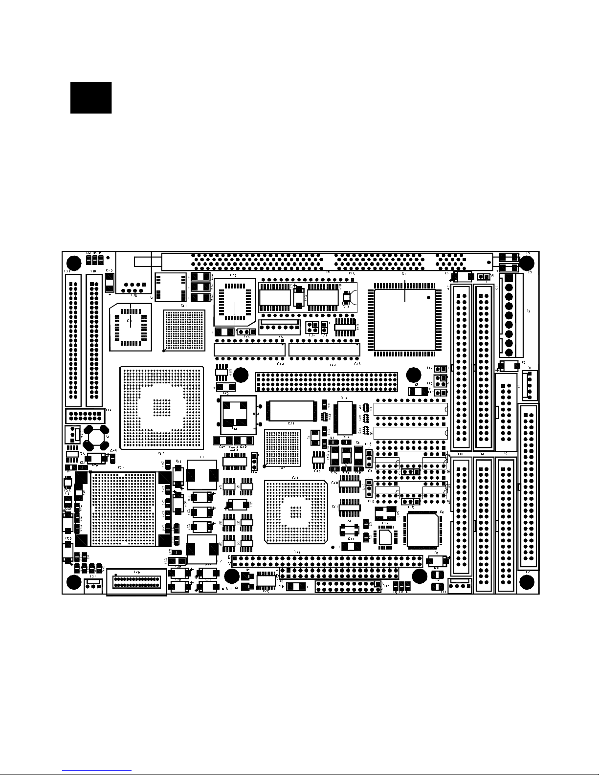
8 AP PEN DIX C
EBC-BX Parts Place ment Guide - Top
030923 OPERATIONS MANUAL EBC-BX Page 8 - 1
Page 73
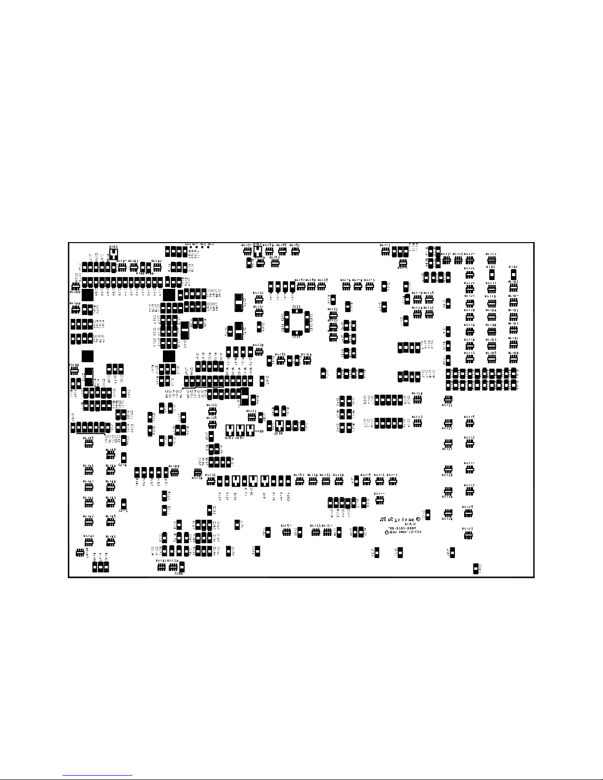
EBC-BX Parts Place ment Guide - Bottom
Page 8 - 2 OPERATIONS MANUAL EBC-BX 030923
Page 74

9 AP PEN DIX D
EBC- BX Parts List
Page 75

10/13/03 Range on Parent Item PAGE 1
11:19:08 WinSystems, Inc.
ASSM ITEM FROM: EBC-BXPLUS-700 ASSM ITEM THRU: EBC-BXPLUS-700
PARENT LOC FROM: <FIRST> DEFAULT COMPONENT LOCATION: ARLIN PARENT LOC THRU: <LAST>
===================================================================================================================================
ITEM QTY
LVL ITEM KEY ITEM DESCRIPTION BOM COMMENT TYPE REQUIRED
===================================================================================================================================
EBC-BXPLUS-700 EBX-COMPATIBLE 700 MHZ LP PENTIUM 3 OMB EBX-COMPATIBLE 700 MHZ LP PENTIUM 3 OMB SD F 1.0
1 999-9999-001 SPECIAL NOTES 07/24/03 MEB ECO 03-44 I 1.0
1 999-9999-001 SPECIAL NOTES 09/11/02 MEB ECO 02-42 I 1.0
1 999-9999-001 SPECIAL NOTES 05/21/02 MEB (REV A) I 1.0
1 999-9999-001 SPECIAL NOTES SPECIAL NOTES I 1.0
1 999-9999-001 SPECIAL NOTES SPECIAL NOTES I 1.0
1 0307-001-0000C ASSY CORE, BOT-SMT EBC-BX REV.C ASSY CORE, BOT-SMT EBC-BX REV.C F 1.0
2 999-9999-001 SPECIAL NOTES 07/24/03 MEB ECO 03-44 REVC I 1.0
2 999-9999-001 SPECIAL NOTES 09/11/02 MEB ECO 02-42 I 1.0
2 999-9999-001 SPECIAL NOTES 05/02/02 MEB (REVA) I 1.0
2 999-9999-001 SPECIAL NOTES 02-06-03 KMT ECO 03-09 I 1.0
2 999-9999-001 SPECIAL NOTES 05/08/03 KMT ECO# 03-36 I 1.0
2 400-0307-000C PCB, EBC-BX REV.C I 1.0
2 601-0000-503 RES 0 Ohm 5% 1/10w 0805 R100,R101,R110,R111,R118,R182,W100, I 13.0
2 999-9999-001 SPECIAL NOTES W105,W107,W109,W112,W113,W114 I 1.0
2 601-0100-503 RES 10 Ohm 5% 1/10w 0805 R149,R165,R166,R167 I 4.0
2 601-0101-503 RES 100 Ohm 5% 1/10w 0805 R127,R139,R183 I 3.0
2 601-0102-503 RES 1K Ohm 5% 1/10W 0805 R128,R130,R131,R137,R138,R140,R144,R151, I 11.0
2 999-9999-001 SPECIAL NOTES R154,R171,R180 I 1.0
2 601-0103-503 RES 10K Ohm 5% 1/10W 0805 R126,R129,R132,R134,R135,R146,R150,R155, I 12.0
2 999-9999-001 SPECIAL NOTES R187,R188,R191,R204 I 1.0
2 601-0203-503 RES 20K Ohms 5% 1/10W 0805 R156 I 1.0
2 601-0220-503 RES 22 Ohm 5% 1/10w 0805 R174,R177,R186 I 3.0
2 601-0271-503 RES 270 Ohm 5% 1/10w 0805 R175,R190,R196 I 3.0
2 601-0303-503 RES 30K OHM 5% 0805 1/10W SMT R152,R160,R205 I 3.0
2 601-0331-503 RES 330 Oh, 5%, 0805 R121,R122,R123,R124,R141,R143,R145,R148, I 12.0
2 999-9999-001 SPECIAL NOTES R195,R197,R199,R202 I 1.0
2 601-0332-503 RES 3.3K Ohm, 5%, 0805 1/10W SMT R158,R162,R176 I 3.0
2 601-0470-503 RES 47 Ohm 5% 1/10w 0805 R170,R194 I 2.0
2 601-0471-503 RES 470 Ohm 20% 1/10w 0805 R102,R107 I 2.0
2 601-0474-503 RES 470K Ohm 5% 1/10W 0805 R120 I 1.0
2 601-0564-503 RES 560K Ohm 5% 1/10W 0805 R119 I 1.0
2 601-0683-503 RESISTOR 68K 5% 0805 SMT R153 I 1.0
2 601-0750-503 RES 75 Ohm 5% 1/10W 0805 R193 I 1.0
2 601-1000-303 RES 100 Ohm 1% 1/10w 0805 SMT R161,R172,R181 I 3.0
2 601-1001-303 RES 1K OHM 1% 1/10W SMT 0805 R185,R201,R203 I 3.0
2 601-1100-303 RES 110 OHM 1% 0805 1/10W SMT R168 I 1.0
2 601-1210-303 RES 121 Ohm 1% 1/10w 0805 R173 I 1.0
2 601-1432-303 RES 14.3K Ohm 1% 1/10w 0805 R163 I 1.0
2 601-1500-303 RES 150 Ohm 1% 1/10w 0805 R159,R178,R192 I 3.0
2 601-1501-303 RES 1.5K Ohm 1% 1/10w 0805 R125,R136,R184 I 3.0
2 601-3922-303 RES 39.2K Ohms 1% 1/10W 0805 R198 I 1.0
2 601-4532-303 RES 45.3K 1% 0805 R164,R200 I 2.0
2 601-5490-303 RES 549 Ohms 1% 0805 R142,R157 I 2.0
2 601-562A-303 RES 56.2 OHM 1% 0805 1/10W SMT R169,R179,R189 I 3.0
2 601-6040-303 RES 604 Ohms 1% 1/10W 0805 R147 I 1.0
10/13/03 Range on Parent Item PAGE 2
11:19:09 WinSystems, Inc.
ASSM ITEM FROM: EBC-BXPLUS-700 ASSM ITEM THRU: EBC-BXPLUS-700
PARENT LOC FROM: <FIRST> DEFAULT COMPONENT LOCATION: ARLIN PARENT LOC THRU: <LAST>
===================================================================================================================================
ITEM QTY
LVL ITEM KEY ITEM DESCRIPTION BOM COMMENT TYPE REQUIRED
===================================================================================================================================
2 602-0100-524 RN 10 Ohm, 5%, 4RES ARRAY RP170,RP198 I 2.0
2 602-0101-524 RN 100 Ohm, 5%, 4RES ARRAY RP150 I 1.0
2 602-0102-524 RN 1K Ohm, 5%, 4RES ARRAY RP105,RP121,RP139,RP141,RP154,RP163,RP173, I 10.0
2 999-9999-001 SPECIAL NOTES RP184,RP199,RP200 I 1.0
2 602-0103-524 RN 10K Ohm, 5%, 4RES ARRAY RP100,RP101,RP102,RP103,RP104,RP113, I 37.0
2 999-9999-001 SPECIAL NOTES RP114,RP115,RP116,RP125,RP126,RP128,RP129, I 1.0
2 999-9999-001 SPECIAL NOTES RP130,RP131,RP132,RP133,RP134,RP135, I 1.0
2 999-9999-001 SPECIAL NOTES RP136,RP137,RP138,RP143,RP144,RP145,RP146, I 1.0
2 999-9999-001 SPECIAL NOTES RP147,RP149,RP157,RP159,RP160,RP161, I 1.0
2 999-9999-001 SPECIAL NOTES RP164,RP165,RP167,RP171,RP172 I 1.0
2 602-0151-524 RN 15O OHM 4 RES 8 PIN PKG 5% RP182,RP183 I 2.0
2 602-0152-524 RN 1.5K OHM 4 RESISTOR 8 PIN PKG RP174 I 1.0
2 602-0220-524 RN 22 Ohm, 5%, 4RES ARRAY RP185,RP186,RP187,RP188,RP189,RP190,RP191 I 11.0
2 999-9999-001 SPECIAL NOTES RP192,RP193,RP194,RP195 I 1.0
2 602-0272-524 RN 2.7K Ohm, 5%, 4RES ARRAY RP142,RP155,RP158,RP162 I 4.0
2 602-0330-524 RN 33 Ohm, 5%, 4RES ARRAY RP106,RP107,RP108,RP109,RP111,RP112,RP117, I 16.0
Page 76

2 999-9999-001 SPECIAL NOTES RP118,RP119,RP120,RP122,RP123,RP124,RP127, I 1.0
2 602-0331-524 RN 330 Ohm, 5%, 4RES ARRAY RP151,RP152 I 2.0
2 602-0471-524 RN 470 Ohm, 4 RES 8 PIN RPACK RP168,RP169 I 2.0
2 602-0472-524 RN 4.7K Ohm, 5%, 4RES ARRAY RP110,RP140,RP148,RP166,RP197 I 5.0
2 602-0750-524 RN 75 Ohm, 5%, 4RES ARRAY RP181,RP196 I 2.0
2 602-0822-524 RN 8.2K Ohm, 5%, 4RES ARRAY RP153,RP156,RP175,RP176,RP177,RP178,RP179, I 8.0
2 999-9999-001 SPECIAL NOTES RP180 I 1.0
2 603-1027-803 CAP 1000pF 50v 20% CER 0805 C111,C272 I 2.0
2 603-1037-803 CAP .01uF 50v 20% CER 0805 C155,C168,C176,C209 I 4.0
2 603-1047-803 CAP .1uF 50v 20% CER 0805 C102,C105,C106,C107,C108,C109,C113,C114, I 109.0
2 999-9999-001 SPECIAL NOTES C115,C116,C117,C118,C119,C120,C121,C122, I 1.0
2 999-9999-001 SPECIAL NOTES C123,C124,C125,C126,C127,C128,C129,C130, I 1.0
2 999-9999-001 SPECIAL NOTES C131,C132,C133,C134,C135,C136,C137,C138, I 1.0
2 999-9999-001 SPECIAL NOTES C139,C140,C141,C142,C143,C144,C145,C146, I 1.0
2 999-9999-001 SPECIAL NOTES C147,C149,C151-C154,C156,C157,C158,C159, I 1.0
2 999-9999-001 SPECIAL NOTES C160,C161,C162,C163,C164,C165,C167,C170, I 1.0
2 999-9999-001 SPECIAL NOTES C172,C178,C179,C180,C183,C184,C185,C186, I 1.0
2 999-9999-001 SPECIAL NOTES C187,C188,C189,C190,C191,C192,C205,C210, I 1.0
2 999-9999-001 SPECIAL NOTES C214,C221,C223,C229,C231,C232,C233,C234, I 1.0
2 999-9999-001 SPECIAL NOTES C236,C237,C239,C240,C241,C242,C243,C247, I 1.0
2 999-9999-001 SPECIAL NOTES C250,C251,C252,C253,C255,C256,C257,C258, I 1.0
2 999-9999-001 SPECIAL NOTES C260,C261,C262,C263,C264,C267,C274,C284, I 1.0
2 999-9999-001 SPECIAL NOTES C285 I 1.0
2 603-1052-803 CAP 1uF 10v 20% CER 0805 C166,C182,C222 I 3.0
2 603-1055-807 CAP 1uF 25v 20% CER 1812 C171,C173,C174,C206,C273 I 5.0
2 603-1061-803 CAP 10uF 6.3v 20% X5R SMT 0805 C150 I 1.0
2 603-1527-803 CAP .0015uF 50v 20% CER 0805 C230 I 1.0
2 603-2219-803 CAP 220pF 200v 20% CER 0805 C278,C282,C286 I 3.0
2 603-8217-803 CAP 820pF 50v 20% CER 0805 C181,C196 I 2.0
2 603-3307-503 CAP 33pF 50v 2% CER 0805 C283 I 1.0
10/13/03 Range on Parent Item PAGE 3
11:19:10 WinSystems, Inc.
ASSM ITEM FROM: EBC-BXPLUS-700 ASSM ITEM THRU: EBC-BXPLUS-700
PARENT LOC FROM: <FIRST> DEFAULT COMPONENT LOCATION: ARLIN PARENT LOC THRU: <LAST>
===================================================================================================================================
ITEM QTY
LVL ITEM KEY ITEM DESCRIPTION BOM COMMENT TYPE REQUIRED
===================================================================================================================================
2 603-3317-803 CAP 330PF 20% 50V 0805 SMT X7R C177,C197 I 2.0
2 603-4707-803 CAP 47pF 50v 20% CER 0805 4k per reel C110,C112,C265,C268,C271 I 5.0
2 603-4737-803 CAP .047uF 50v 20% CER 0805 C148,C169 I 2.0
2 603-56R7-303 CAP 5.6pF 50V +/-.5PF 0805 SMT NPO C175,C193 I 2.0
2 603-82R7-303 CAP 8.2pF 50v .50pF CER 0805 C220 I 1.0
2 607-0008-000 DIODE SMT SCHOTTKY SOT-23 D100,D101,D102 I 3.0
2 660-0002-002 TRANS MMBT2222ALT1 SOT-23 Q100,Q101,Q103,Q104 I 4.0
2 665-0004-002 FAIRCHILD FDV301N NCHANNEL DIGITAL FET Q102 I 1.0
----------------------------------------------------------------------------------------------------------------------------------SUB-ASSEMBLY TOTAL: 0307-001-0000C ARLIN - 93 Items
---------------------------------------------------------------------------------------------------------------------------------- 1 0307-002-0000C ASSY CORE, TOP-TH EBC-BX REV.C ASSY CORE, TOP-TH EBC-BX REV.C F 1.0
2 999-9999-001 SPECIAL NOTES 07/24/03 MEB ECO 03-44 I 1.0
2 999-9999-001 SPECIAL NOTES 07-01-03 MEB ECO 03-36 I 1.0
2 999-9999-001 SPECIAL NOTES 09/11/02 MEB ECO 02-42 I 1.0
2 999-9999-001 SPECIAL NOTES 05/15/02 MEB (REVA) I 1.0
2 999-9999-001 SPECIAL NOTES SPECIAL NOTES I 1.0
2 999-9999-001 SPECIAL NOTES SPECIAL NOTES I 1.0
2 200-0040-000 SOCKET 40 POS QPHFZ-40-B-1W (Aptos) J20 I 1.0
2 200-0064-000 SOCKET 64 POS QPHFZ-64-B-1W (Aptos) J23 I 1.0
2 200-0120-000 CONN PC104 PLUS Aptos PQECOK9.35/2.28 J22 I 1.0
2 200-0168-100 SOCKET 168 PIN 3.0V SDRAM DIMM,VERTICAL M1 I 1.0
2 201-0003-001 HDR 3 PIN MOLEX 22-11-2032 J31,J34 I 2.0
2 201-0004-003 HDR MOLEX 4 POS 22-11-2042 J11 I 1.0
2 201-0005-003 HEADER 5 PIN LATCH MOLEX 22-11-2052 J1 I 1.0
2 201-0009-003 HEADER 9 POS. RA .156" SP GOLD PLATING J3 I 1.0
2 201-0034-021 HDR 34 ST IDH-34LP-S3-TR (720) J10 I 1.0
2 201-0036-010 HDR 1X36 UN Aptos LHY-36S-E-060/030 J12,J21=1X2 I .6
2 999-9999-001 SPECIAL NOTES J15,J16,J17,J18,J27=1X3 I 1.0
2 201-0040-022 HDR 40 POS IDC W/PIN 20 REMOVED 80/tray J5,J8 I 2.0
2 201-0050-021 HDR 50 ST IDH-50LP-S3-TR (504) 60/tray: J2 I 1.0
2 201-0072-120 HDR 2X36 UN Aptos LHZ-72S-E-060/030 J13=2X2 J19=2X11 I .4
2 250-0320-001 TERMINAL STRIP 316-93-132-41-006000 U15=2X16 I 1.0
2 250-0320-200 SKT STRP 32 POS SS-132-G-2 (SAM) U4,U6=2X12 U5,U7,U9,U10=2X4 I 3.0
2 200-0243-100 SOCKET 24 P .3 ICO-243-S8A-T (1,496) U17,U28 I 2.0
----------------------------------------------------------------------------------------------------------------------------------SUB-ASSEMBLY TOTAL: 0307-002-0000C ARLIN - 23 Items
---------------------------------------------------------------------------------------------------------------------------------- 1 0307-004-0000C ASSY CORE, TOP-SMT EBC-BX REV.C ASSY CORE, TOP-SMT EBC-BX REV.C F 1.0
2 999-9999-001 SPECIAL NOTES 07/24/03 MEB ECO 03-44 I 1.0
Page 77

2 999-9999-001 SPECIAL NOTES 09/11/02 MEB ECO 02-42 I 1.0
2 999-9999-001 SPECIAL NOTES 05/15/02 MEB (REVA) I 1.0
2 999-9999-001 SPECIAL NOTES SPECIAL NOTES I 0.0
2 999-9999-001 SPECIAL NOTES SPECIAL NOTES I 1.0
2 125-0008-000 TRANSISTOR SI4947DY DUAL P-CHANNEL FET U29 I 1.0
2 601-0220-503 RES 22 Ohm 5% 1/10w 0805 R1,R2 I 2.0
10/13/03 Range on Parent Item PAGE 4
11:19:11 WinSystems, Inc.
ASSM ITEM FROM: EBC-BXPLUS-700 ASSM ITEM THRU: EBC-BXPLUS-700
PARENT LOC FROM: <FIRST> DEFAULT COMPONENT LOCATION: ARLIN PARENT LOC THRU: <LAST>
===================================================================================================================================
ITEM QTY
LVL ITEM KEY ITEM DESCRIPTION BOM COMMENT TYPE REQUIRED
===================================================================================================================================
2 601-2508-304 RES .025 OHM 1/2WATT 1% 1206 SMT R4 I 1.0
2 602-0330-524 RN 33 Ohm, 5%, 4RES ARRAY RP1,RP2,RP3,RP4 I 4.0
2 603-1047-803 CAP .1uF 50v 20% CER 0805 C10,C15,C36,C42-C46,C48,C50,C56 I 11.0
2 603-1055-807 CAP 1uF 25v 20% CER 1812 C38,C53 I 2.0
2 603-1065-82D CAP 10uF 25v 20% TAN 6032 C1,C2,C9,C11,C14,C19,C20,C24 I 8.0
2 603-107C-85F CAP 100UF 8VOLT 20% POLYMER ALUM 7343H C3,C21,C30,C31,C32,C33,C34 I 7.0
2 603-187B-85F IC, CAP 180UF 4V 20% POLYMER ALUM 7343H C25,C26,C39,C40,C49,C60 I 6.0
2 603-2207-503 CAP 22PF 50v 2% NPO 0805 C12,C13,C16,C17 I 4.0
2 603-3365-82E CAP 33UF 25V 20% 7343 TANT.SMT C5,C59 I 2.0
2 603-4763-82E CAP 47uF 16v 20% TAN 7343 C4,C18 I 2.0
2 603-68R7-203 CAP 6.8pF 50v +/-.5pf CER 0805 4k/reel C7,C8 I 2.0
2 605-1005-000 INDUCTOR 4.7uh 0805 SMT L3 I 1.0
2 605-2001-000 FERRITE BEAD, SMT 3528 FB1,FB2 I 2.0
2 606-0006-000 IC, 5VH 4AMP TRANSFORMER T2 I 1.0
2 606-0008-000 IC, SHIELDED INDUCTOR SMT L1,L2 I 2.0
2 607-0005-005 LED, GREEN SMT D1,D7 I 2.0
2 607-0006-005 LED, RED SMT D2,D3,D6 I 3.0
2 607-0007-005 LED, YELLOW SMT D8 I 1.0
2 607-0010-013 IC UPS5819 POWERMITE SCHOTTKY DIODE 1A D4,D5 I 2.0
2 611-0004-001 IC, 74HC04M Philips 74HC04D-T 2500/reel U20 I 1.0
2 611-0125-001 IC, 74HC125 QUAD TRI-STATE BUFFER U16 I 1.0
2 611-0245-002 IC, 74HC245DW-T Philips 2k/reel U22 I 1.0
2 612-0014-001 IC, 74HCT14 (SM) U21 I 1.0
2 612-0688-002 IC, 74HCT688D-T (SM) Philips 2k/reel U14 I 1.0
2 621-0025-024 IC, FDC37C672-MD SUPER I/O TQFP U8 I 1.0
2 622-0002-019 IC, LTC1726EMS8-5 SUPERVISOR U13 I 1.0
2 622-0020-021 IC, SYSTEM HARDWARE MONITOR U26 I 1.0
2 622-0021-019 IC, FREQ. SYNTH CY28317ZC-2T TSSOP U18 I 1.0
2 623-0011-025 IC, INTEL 82443BX HOST BRIDGE/CONTROLLER U32 I 1.0
2 623-0012-025 IC, SMSC SLC90E66 PCI SOUTH BRIDGE U25 I 1.0
2 650-0032-002 SOCKET 32P AMP 822498-1 (28) U27 I 1.0
2 665-0005-008 IC, N CHANNEL SMPS MOSFET S0-8 PKG Q1,Q2,Q3,Q4,Q5,Q6 I 6.0
2 668-0001-008 IC, DUAL COMPLIMENTARY MOSFET S0-8 PKG U35 I 1.0
2 677-0006-029 IC, SWITCHING REGULATOR CONTROLLER U36 I 1.0
2 677-0007-019 IC, DUAL SWITCHING CONT. W/150ma LD0 U37 I 1.0
2 681-0002-007 XTAL, 14.31818mhz 18pf SMT FA-365 Y2 I 1.0
2 681-0004-001 XTAL 32.768KHZ SMT 6pf load capacity Y1 I 1.0
2 682-0003-006 OSC 1.8432MHZ CMOS SG-710 SERIES U11 I 1.0
2 690-0001-000 TRANSDUCER, AUDIO STAR MQT-03D SP1 I 1.0
----------------------------------------------------------------------------------------------------------------------------------SUB-ASSEMBLY TOTAL: 0307-004-0000C ARLIN - 46 Items
---------------------------------------------------------------------------------------------------------------------------------- 1 0307-010-0000C SUB ASSY CORE, EBC-BX REV.C SUB ASSY CORE, EBC-BX REV.C F 1.0
2 999-9999-001 SPECIAL NOTES 07/24/03 MEB ECO 03-44 I 1.0
2 999-9999-001 SPECIAL NOTES 09/11/02 MEB ECO 02-42 I 1.0
2 999-9999-001 SPECIAL NOTES 05/15/02 MEB (REVA) I 1.0
10/13/03 Range on Parent Item PAGE 5
11:19:12 WinSystems, Inc.
ASSM ITEM FROM: EBC-BXPLUS-700 ASSM ITEM THRU: EBC-BXPLUS-700
PARENT LOC FROM: <FIRST> DEFAULT COMPONENT LOCATION: ARLIN PARENT LOC THRU: <LAST>
===================================================================================================================================
ITEM QTY
LVL ITEM KEY ITEM DESCRIPTION BOM COMMENT TYPE REQUIRED
===================================================================================================================================
2 999-9999-001 SPECIAL NOTES 02-05-03 KMT ECO 0309 I 1.0
2 999-9999-001 SPECIAL NOTES SPECIAL NOTES I 1.0
2 999-9999-001 SPECIAL NOTES SPECIAL NOTES I 1.0
2 111-0047-000 BATTERY, LTC-3PN 3.5V (EAGLE PICHER) BT1 *MUST HAND SOLDER AFTER ASSEMBLY I 1.0
Page 78

2 201-0002-000 PLUG JUMPER 999-19-310-00-000000 J12=1-2 J13=1-2 3-4 I 9.0
2 999-9999-001 SPECIAL NOTES J19=5-6 11-12 13-14 19-20 21-22 I 1.0
2 999-9999-001 SPECIAL NOTES J27=2-3 I 1.0
2 637-0008-015 FLASH, 256KX8 AT29C020-PLCC (32/TUBE) U27 CS=4A9B \EBCBX\REL0416.BIN I 1.0
2 730-0083-000 IC, SP208CP (SIPEX), MAX208CNG (15) U4,U6 I 2.0
2 901-0011-000 IC, PALC22V10-35PC (15,TI) (17,CYP) U17 CS=8503 \EBCBX\EBCBXU17.JED I 2.0
2 999-9999-001 SPECIAL NOTES U28 CS=2B84 \EBCBX\EBCBXU28.JED I 1.0
2 999-9999-001 SPECIAL NOTES NOTE: INST. FOR ASSY. OF FAN / HEAT SINK I 1.0
2 403-0307-200 ASSY DRAWING, CPU COOLER DRAWING, CPU COOLER INSTRUCTIONS. I 1.0
2 502-0515-200 CPU COOLER, 54mm 5V W/TACH 10 wk LT U34 * SEE 403-0307-200 INSTRUCTIONS I 1.0
2 502-0009-000 HEAT SINK 1" X 1" MATERIAL/PART# RD-339C U34 * SEE 403-0307-200 INSTRUCTIONS I 1.0
2 502-0018-000 HEAT 'SPREADER' 1.25"x 1.60" COPPER U34 * SEE 403-0307-200 INSTRUCTIONS I 1.0
2 502-0209-000 HEAT SINK .750"x.750" THERMAGAP .020"THK U34 * SEE 403-0307-200 INSTRUCTIONS I 1.0
2 500-0200-033 SCREW PPH 4-40 X 1/4" U34 * SEE 403-0307-200 INSTRUCTIONS I 4.0
2 CBL-238-1 CABLE, CPU COOLING FAN U34 * SEE 403-0307-200 INSTRUCTIONS I 1.0
2 502-0016-000 HEAT SINK,BDN14-3CB 1.41"SQUARE x.355"HT U32 * INST. W/THERMAL ADHESIVE 502-0009-00 I 1.0
2 502-0009-000 HEAT SINK 1" X 1" MATERIAL/PART# RD-339C U32 * INST. ON 502-0016-000 I 1.0
----------------------------------------------------------------------------------------------------------------------------------SUB-ASSEMBLY TOTAL: 0307-010-0000C ARLIN - 24 Items
---------------------------------------------------------------------------------------------------------------------------------- 1 0307-200-0000C ASSY ENET, TOP-SMT, EBC-BX REV.C ASSY ENET, TOP-SMT, EBC-BX REV.C F 1.0
2 999-9999-001 SPECIAL NOTES 07/24/03 MEB ECO 03-44 I 1.0
2 999-9999-001 SPECIAL NOTES 09/11/02 MEB ECO 02-42 I 1.0
2 999-9999-001 SPECIAL NOTES 05/16/02 MEB (REVA) I 1.0
2 999-9999-001 SPECIAL NOTES 12/06/02 KT ECO# 02-73 I 1.0
2 999-9999-001 SPECIAL NOTES SPECIAL NOTES I 1.0
2 999-9999-001 SPECIAL NOTES SPECIAL NOTES I 1.0
2 603-1065-82D CAP 10uF 25v 20% TAN 6032 C22 I 1.0
2 606-0007-000 IC, 10/100 LAN MAGNETICS T1 I 1.0
2 621-0038-025 IC, GD82551QM ETHERNET PCI CONTROLLER U24 I 1.0
2 635-0001-001 IC, 24C02 SEEPROM S08 SERIAL 16X64 U19 I 1.0
2 681-0001-007 XTAL, 25.0000mhz 18pf SMT FA-365 Y3 I 1.0
----------------------------------------------------------------------------------------------------------------------------------SUB-ASSEMBLY TOTAL: 0307-200-0000C ARLIN - 11 Items
---------------------------------------------------------------------------------------------------------------------------------- 1 0307-202-0000C ASSY ENET, TOP-TH EBC-BX REV.C ASSY ENET, TOP-TH EBC-BX REV.C F 1.0
2 999-9999-001 SPECIAL NOTES 07/24/03 MEB ECO 03-44 I 1.0
2 999-9999-001 SPECIAL NOTES 09/11/02 MEB ECO 02-42 I 1.0
2 999-9999-001 SPECIAL NOTES 05/16/02 MEB (REVA) I 1.0
2 999-9999-001 SPECIAL NOTES SPECIAL NOTES I 1.0
2 999-9999-001 SPECIAL NOTES SPECIAL NOTES I 1.0
2 201-0008-500 TEL JACK RJ45 MOLEX 950-01-2881 J28 I 1.0
----------------------------------------------------------------------------------------------------------------------------------SUB-ASSEMBLY TOTAL: 0307-202-0000C ARLIN - 6 Items
-----------------------------------------------------------------------------------------------------------------------------------
10/13/03 Range on Parent Item PAGE 6
11:19:13 WinSystems, Inc.
ASSM ITEM FROM: EBC-BXPLUS-700 ASSM ITEM THRU: EBC-BXPLUS-700
PARENT LOC FROM: <FIRST> DEFAULT COMPONENT LOCATION: ARLIN PARENT LOC THRU: <LAST>
===================================================================================================================================
ITEM QTY
LVL ITEM KEY ITEM DESCRIPTION BOM COMMENT TYPE REQUIRED
===================================================================================================================================
1 0307-300-0000C ASSY VIDEO,TOP-SMT EBC-BX REV.C ASSY VIDEO,TOP-SMT EBC-BX REV.C F 1.0
2 999-9999-001 SPECIAL NOTES 07/24/03 MEB ECO 03-44 I 1.0
2 999-9999-001 SPECIAL NOTES 09/11/02 MEB ECO 02-42 I 1.0
2 999-9999-001 SPECIAL NOTES 05/16/02 MEB (REVA) I 1.0
2 999-9999-001 SPECIAL NOTES SPECIAL NOTES I 1.0
2 999-9999-001 SPECIAL NOTES SPECIAL NOTES I 1.0
2 603-1065-82D CAP 10uF 25v 20% TAN 6032 C23,C27,C28,C29,C47 I 5.0
2 650-0032-002 SOCKET 32P AMP 822498-1 (28) U33 I 1.0
2 621-0026-025 IC, VIDEO CONTROLLER, 69K 256 PIN MBGA U31 I 1.0
----------------------------------------------------------------------------------------------------------------------------------SUB-ASSEMBLY TOTAL: 0307-300-0000C ARLIN - 8 Items
---------------------------------------------------------------------------------------------------------------------------------- 1 0307-302-0000C ASSY VIDEO,TOP-THR EBC-BX REV.C ASSY VIDEO,TOP-THR EBC-BX REV.C F 1.0
2 999-9999-001 SPECIAL NOTES 07/24/03 MEB ECO 03-44 I 1.0
2 999-9999-001 SPECIAL NOTES 09/11/02 MEB ECO 02-42 I 1.0
2 999-9999-001 SPECIAL NOTES 05/16/02 MEB (REVA) I 1.0
2 999-9999-001 SPECIAL NOTES SPECIAL NOTES I 1.0
2 999-9999-001 SPECIAL NOTES SPECIAL NOTES I 1.0
2 201-0007-003 HEADER 7 PIN MOLEX 22-11-2072 J25 I 1.0
2 201-0014-420 HDR., 2X7 2MM SHROUDED J32 I 1.0
2 201-0036-010 HDR 1X36 UN Aptos LHY-36S-E-060/030 J26=1X3 I 1.0
2 201-0050-420 HDR, Sam., STMM-125-02-S-D J30,J33 I 2.0
----------------------------------------------------------------------------------------------------------------------------------SUB-ASSEMBLY TOTAL: 0307-302-0000C ARLIN - 9 Items
---------------------------------------------------------------------------------------------------------------------------------- 1 0307-310-0000C SUB ASSY VIDEO, EBC-BX REV.C SUB ASSY VIDEO, EBC-BX REV.C F 1.0
2 999-9999-001 SPECIAL NOTES 07/24/03 MEB ECO 03-44 I 1.0
2 999-9999-001 SPECIAL NOTES 03/21/03 MEB ECO 03-20 I 1.0
Page 79

2 999-9999-001 SPECIAL NOTES 09/11/02 MEB ECO 02-42 I 1.0
2 999-9999-001 SPECIAL NOTES 05/16/02 MEB (REVA) I 1.0
2 999-9999-001 SPECIAL NOTES SPECIAL NOTES I 1.0
2 999-9999-001 SPECIAL NOTES SPECIAL NOTES I 1.0
2 637-0003-015 IC, AT29C010A-12JC 128K X 8 FLASH ROM U33 CS=3B00 EBCBX\PCIVID\REL0314.BIN I 1.0
2 201-0002-000 PLUG JUMPER 999-19-310-00-000000 J12=1-2 I 2.0
2 999-9999-001 SPECIAL NOTES J26=2-3 I 1.0
----------------------------------------------------------------------------------------------------------------------------------SUB-ASSEMBLY TOTAL: 0307-310-0000C ARLIN - 9 Items
---------------------------------------------------------------------------------------------------------------------------------- 1 0307-400-0000C ASSY SECOND SERIAL TOP-SMT,EBC-BX REVC ASSY SECOND SERIAL TOP-SMT,EBC-BX REVC F 1.0
2 999-9999-001 SPECIAL NOTES 07/24/03 MEB ECO 03-44 I 1.0
2 999-9999-001 SPECIAL NOTES 09/11/02 MEB ECO 02-42 I 1.0
2 999-9999-001 SPECIAL NOTES 05/16/02 MEB (REVA) I 1.0
2 999-9999-001 SPECIAL NOTES SPECIAL NOTES I 1.0
2 999-9999-001 SPECIAL NOTES SPECIAL NOTES I 1.0
2 621-0033-024 IC, ST16C2550CQ48 DUAL UART U12 I 1.0
----------------------------------------------------------------------------------------------------------------------------------SUB-ASSEMBLY TOTAL: 0307-400-0000C ARLIN - 6 Items
-----------------------------------------------------------------------------------------------------------------------------------
10/13/03 Range on Parent Item PAGE 7
11:19:14 WinSystems, Inc.
ASSM ITEM FROM: EBC-BXPLUS-700 ASSM ITEM THRU: EBC-BXPLUS-700
PARENT LOC FROM: <FIRST> DEFAULT COMPONENT LOCATION: ARLIN PARENT LOC THRU: <LAST>
===================================================================================================================================
ITEM QTY
LVL ITEM KEY ITEM DESCRIPTION BOM COMMENT TYPE REQUIRED
===================================================================================================================================
1 0307-402-0000C ASSY SECOND SERIAL TOP-TH,EBC-BX REV.C ASSY SECOND SERIAL TOP-TH,EBC-BX REV.C F 1.0
2 999-9999-001 SPECIAL NOTES 07/24/03 MEB ECO 03-44 I 1.0
2 999-9999-001 SPECIAL NOTES 09/11/02 MEB ECO 02-42 I 1.0
2 999-9999-001 SPECIAL NOTES 05/16/02 MEB (REVA) I 1.0
2 999-9999-001 SPECIAL NOTES SPECIAL NOTES I 1.0
2 999-9999-001 SPECIAL NOTES SPECIAL NOTES I 1.0
2 201-0020-021 HEADER 2x10 ST Aptos LPHS-20S3-B-032-SP J4 I 1.0
2 201-0072-120 HDR 2X36 UN Aptos LHZ-72S-E-060/030 J24=2X2 I .1
2 250-0320-200 SKT STRP 32 POS SS-132-G-2 (SAM) U2=2X12 U3=2X12 I .7
----------------------------------------------------------------------------------------------------------------------------------SUB-ASSEMBLY TOTAL: 0307-402-0000C ARLIN - 8 Items
---------------------------------------------------------------------------------------------------------------------------------- 1 0307-410-0000C SUB ASSY SECOND SERIAL,EBC-BX REV.C SUB ASSY SECOND SERIAL,EBC-BX REV.C F 1.0
2 999-9999-001 SPECIAL NOTES 07/24/03 MEB ECO 03-44 I 1.0
2 999-9999-001 SPECIAL NOTES 09/11/02 MEB ECO 02-42 I 1.0
2 999-9999-001 SPECIAL NOTES 05/16/02 MEB (REVA) I 1.0
2 999-9999-001 SPECIAL NOTES SPECIAL NOTES I 1.0
2 999-9999-001 SPECIAL NOTES SPECIAL NOTES I 1.0
2 730-0083-000 IC, SP208CP (SIPEX), MAX208CNG (15) U2,U3 I 2.0
2 201-0002-000 PLUG JUMPER 999-19-310-00-000000 J24=1-2 3-4 I 2.0
----------------------------------------------------------------------------------------------------------------------------------SUB-ASSEMBLY TOTAL: 0307-410-0000C ARLIN - 7 Items
---------------------------------------------------------------------------------------------------------------------------------- 1 0307-500-0000C ASSY DIGITAL TOP SMT, EBC-BX REV.C ASSY DIGITAL TOP SMT, EBC-BX REV.C F 1.0
2 999-9999-001 SPECIAL NOTES 07/24/03 MEB ECO 03-44 I 1.0
2 999-9999-001 SPECIAL NOTES 09/11/02 MEB ECO 02-42 I 1.0
2 999-9999-001 SPECIAL NOTES 05/16/02 MEB (REVA) I 1.0
2 999-9999-001 SPECIAL NOTES SPECIAL NOTES I 1.0
2 999-9999-001 SPECIAL NOTES SPECIAL NOTES I 1.0
2 603-1065-82D CAP 10uF 25v 20% TAN 6032 C6 I 1.0
2 650-0084-002 SOCKET, 84 POSITION PLCC 213-084-602 U1 I 1.0
----------------------------------------------------------------------------------------------------------------------------------SUB-ASSEMBLY TOTAL: 0307-500-0000C ARLIN - 7 Items
---------------------------------------------------------------------------------------------------------------------------------- 1 0307-502-0000C ASSY DIGITAL TOP TH, EBC-BX REV.C ASSY DIGITAL TOP TH, EBC-BX REV.C F 1.0
2 999-9999-001 SPECIAL NOTES 07/24/03 MEB ECO 03-44 I 1.0
2 999-9999-001 SPECIAL NOTES 09/11/02 MEB ECO 02-42 I 1.0
2 999-9999-001 SPECIAL NOTES 05/16/02 MEB (REVA) I 1.0
2 999-9999-001 SPECIAL NOTES SPECIAL NOTES I 1.0
2 999-9999-001 SPECIAL NOTES SPECIAL NOTES I 1.0
2 201-0036-010 HDR 1X36 UN Aptos LHY-36S-E-060/030 J6,J14=1X2 I .1
2 201-0050-021 HDR 50 ST IDH-50LP-S3-TR (504) 60/tray: J7,J9 I 2.0
----------------------------------------------------------------------------------------------------------------------------------SUB-ASSEMBLY TOTAL: 0307-502-0000C ARLIN - 7 Items
---------------------------------------------------------------------------------------------------------------------------------- 1 0307-510-0000C SUB ASSY DIGITAL, EBC-BX REV.C SUB ASSY DIGITAL, EBC-BX REV.C F 1.0
Page 80

10/13/03 Range on Parent Item PAGE 8
11:19:15 WinSystems, Inc.
ASSM ITEM FROM: EBC-BXPLUS-700 ASSM ITEM THRU: EBC-BXPLUS-700
PARENT LOC FROM: <FIRST> DEFAULT COMPONENT LOCATION: ARLIN PARENT LOC THRU: <LAST>
===================================================================================================================================
ITEM QTY
LVL ITEM KEY ITEM DESCRIPTION BOM COMMENT TYPE REQUIRED
===================================================================================================================================
2 999-9999-001 SPECIAL NOTES 07/24/03 MEB ECO 03-44 I 1.0
2 999-9999-001 SPECIAL NOTES 09/11/02 MEB ECO 02-42 I 1.0
2 999-9999-001 SPECIAL NOTES 05/16/02 MEB (REVA) I 1.0
2 999-9999-001 SPECIAL NOTES SPECIAL NOTES I 1.0
2 999-9999-001 SPECIAL NOTES SPECIAL NOTES I 1.0
2 201-0002-000 PLUG JUMPER 999-19-310-00-000000 J6=1-2 I 1.0
2 905-0030-000 IC, UD27-PL84-M3B:D U1 I 1.0
----------------------------------------------------------------------------------------------------------------------------------SUB-ASSEMBLY TOTAL: 0307-510-0000C ARLIN - 7 Items
---------------------------------------------------------------------------------------------------------------------------------- 1 0307-720-0000C SUB ASSY BOT-SMT PROCESSOR 700MHZ REVC SUB ASSY BOT-SMT PROCESSOR 700MHZ REVC F 1.0
2 999-9999-001 SPECIAL NOTES 07/24/03 MEB ECO 03-44 I 1.0
2 999-9999-001 SPECIAL NOTES 09/11/02 MEB ECO 02-42 I 1.0
2 999-9999-001 SPECIAL NOTES 05/16/02 MEB (REVA) I 1.0
2 999-9999-001 SPECIAL NOTES SPECIAL NOTES I 1.0
2 999-9999-001 SPECIAL NOTES SPECIAL NOTES I 1.0
2 603-2252-803 CAP 2.2uF X5R 10v 20% CER 0805 C194,C195,C198,C199,C201,C202,C207,C208, I 35.0
2 999-9999-001 SPECIAL NOTES C212,C213,C215,C216,C217,C218,C219,C224, I 1.0
2 999-9999-001 SPECIAL NOTES C225,C226,C227,C228,C235,C238,C244,C245, I 1.0
2 999-9999-001 SPECIAL NOTES C246,C254,C259,C266,C269,C270,C275,C276, I 1.0
2 999-9999-001 SPECIAL NOTES C277,C280,C281 I 1.0
2 601-0000-503 RES 0 Ohm 5% 1/10w 0805 W102,W106 I 2.0
----------------------------------------------------------------------------------------------------------------------------------SUB-ASSEMBLY TOTAL: 0307-720-0000C ARLIN - 11 Items
---------------------------------------------------------------------------------------------------------------------------------- 1 0307-725-0000C SUB ASSY TOP-SMT PROCESSOR 700MHZ REVC SUB ASSY TOP-SMT PROCESSOR 700MHZ REVC F 1.0
2 999-9999-001 SPECIAL NOTES 07/24/03 MEB ECO 03-44 I 1.0
2 999-9999-001 SPECIAL NOTES 09/11/02 MEB ECO 02-42 I 1.0
2 999-9999-001 SPECIAL NOTES 05/16/02 MEB (REVA) I 1.0
2 999-9999-001 SPECIAL NOTES SPECIAL NOTES I 1.0
2 999-9999-001 SPECIAL NOTES SPECIAL NOTES I 1.0
2 603-2252-803 CAP 2.2uF X5R 10v 20% CER 0805 C35,C37,C41,C51,C52,C54,C55,C57,C58 I 9.0
2 620-0017-025 IC, PROC. KC80526GY850256 850MHZ PIII U34 I 1.0
----------------------------------------------------------------------------------------------------------------------------------SUB-ASSEMBLY TOTAL: 0307-725-0000C ARLIN - 7 Items
---------------------------------------------------------------------------------------------------------------------------------- 1 950-0001-100 BAG STATIC BARRIER 07-0810 8X10 BAG STATIC BARRIER 07-0810 8X10 I 1.0
1 910-0024-000 LABEL, STATIC SENSITIVE 130-02 LABEL, STATIC SENSITIVE 130-02 I 1.0
1 910-0037-000 LABEL, AWARD BIOS, D686 Pentium INSTALL BIOS LABEL ON PC104 CONNECTOR. I 1.0
1 999-9999-001 SPECIAL NOTES NOTE: JUMPER SETUP SUMMARY I 1.0
1 999-9999-001 SPECIAL NOTES J6=1-2 I 1.0
1 999-9999-001 SPECIAL NOTES J12=1-2 I 1.0
1 999-9999-001 SPECIAL NOTES J13=1-2, 3-4 I 1.0
1 999-9999-001 SPECIAL NOTES J19=5-6, 11-12, 13-14, 19-20, 21-22 I 1.0
1 999-9999-001 SPECIAL NOTES J24=1-2, 3-4 I 1.0
1 999-9999-001 SPECIAL NOTES J26=2-3 I 1.0
10/13/03 Range on Parent Item PAGE 9
11:19:15 WinSystems, Inc.
ASSM ITEM FROM: EBC-BXPLUS-700 ASSM ITEM THRU: EBC-BXPLUS-700
PARENT LOC FROM: <FIRST> DEFAULT COMPONENT LOCATION: ARLIN PARENT LOC THRU: <LAST>
===================================================================================================================================
ITEM QTY
LVL ITEM KEY ITEM DESCRIPTION BOM COMMENT TYPE REQUIRED
===================================================================================================================================
1 999-9999-001 SPECIAL NOTES J27=2-3 I 1.0
===================================================================================================================================
TOP ASSEMBLY TOTAL: EBC-BXPLUS-700 ARLIN - 33 Items
===================================================================================================================================
REPORT RECAP
----------- 0 WARNING(S)
PARAMETER RECAP
--------------PARAMETER KEY : 10 BOM for Manuals
REPORT TITLE : Range on Parent Item
ASSM ITEM RANGE : EBC-BXPLUS-700 THRU EBC-BXPLUS-700 COSTING METHOD : A
PARENT LOC RANGE : <FIRST> THRU <LAST> QUANTITY TO EXPLODE : 1
Page 81

PRODUCT KEY RANGE : <FIRST> THRU <LAST> USE SCRAP FACTOR (Y/N) : N
COMMODITY KEY RANGE : <FIRST> THRU <LAST> UPDATE INV STD COST : N
NO. LEVELS TO EXPLODE : 999
DEFAULT COMP LOC : ARLIN COLUMNS OF DESC TEXT : 42
BOM STATUS PRIORITY : A SHORT OR LONG (S/L) : S
PRINT ITEM DESC (Y/N) : Y
Page 82

10 AP PEN DIX E
EBC-BX Me chani cal Draw ing
Page 83
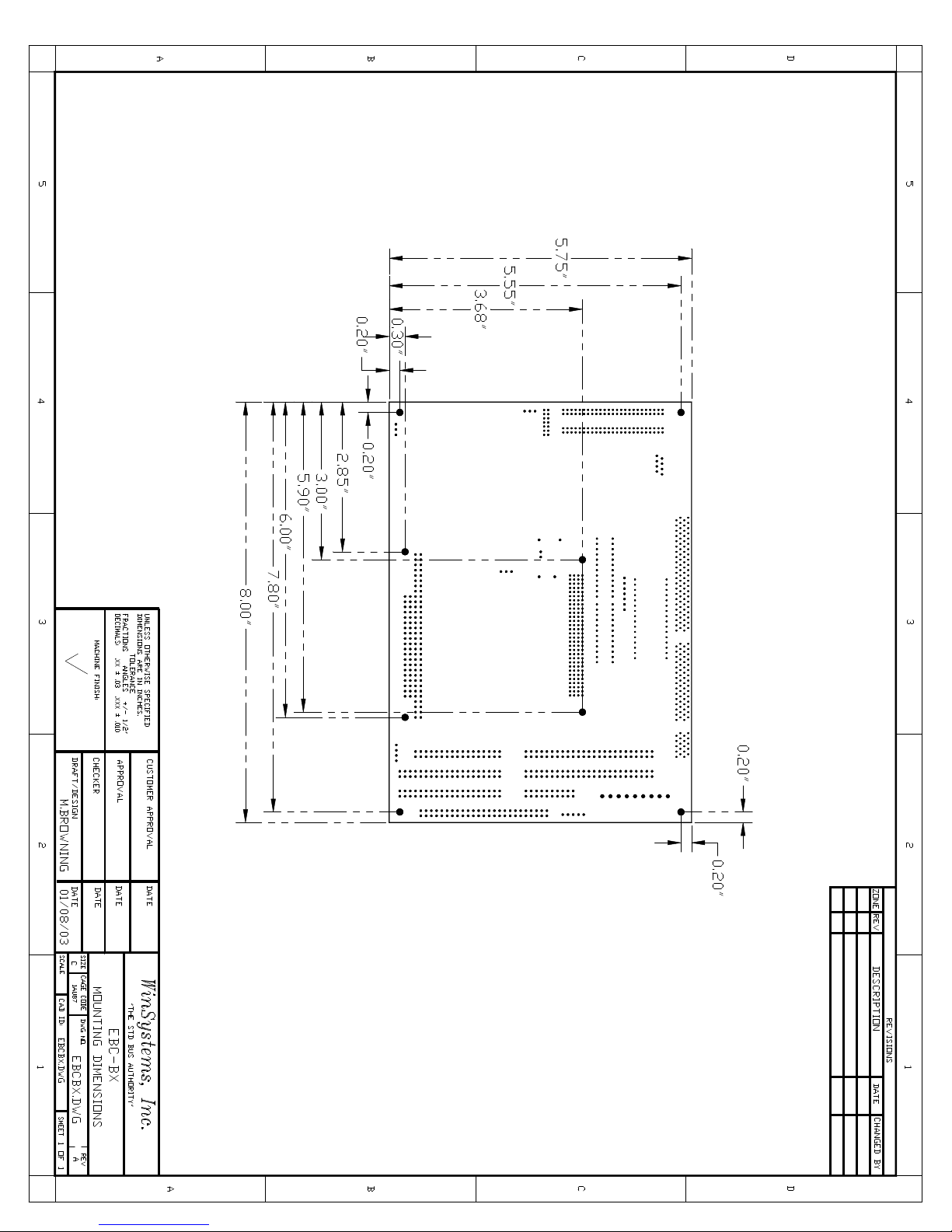
Page 84

11
APPENDIX F
WS16C48 I/O Routines and Sample Program Listings
Page 85

/* UIO48.H
Copyright 1996 by WinSystems Inc.
Permission is hereby granted to the purchaser of the WinSystems
UIO cards and CPU products incorporating the UIO device, to distribute
any binary file or files compiled using this source code directly or
in any work derived by the user from this file. In no case may the
source code, original or derived from this file, be distributed to any
third party except by explicit permission of WinSystems. This file is
distributed on an "As-is" basis and no warranty as to performance,
fitness of purposes, or any other warranty is expressed or implied.
In no case shall WinSystems be liable for any direct or indirect loss
or damage, real or consequential resulting from the usage of this
source code. It is the user's sole responsibility to determine
fitness for any considered purpose.
*/
/**************************************************************************
* Name : uio48.h
*
* Project : PCM-UIO48 Software Samples/Examples
*
* Date : October 30, 1996
*
* Revision: 1.00
*
* Author : Steve Mottin
*
****************************************************************************
*
* Changes :
*
* Date Revision Description
* ________ ________ ______________________________________________
* 10/30/96 1.00 Created
*
*****************************************************************************
*/
#define RISING 1
#define FALLING 0
void init_io(unsigned io_address);
int read_bit(int bit_number);
void write_bit(int bit_number);
void set_bit(int bit_number);
void clr_bit(int bit_number);
void enab_int(int bit_number, int polarity);
void disab_int(int bit_number);
void clr_int(int bit_number);
int get_int(void);
Page 86

/* UIO48.C
Copyright 1996 by WinSystems Inc.
Permission is hereby granted to the purchaser of the WinSystems
UIO cards and CPU products incorporating the UIO device, to distribute
any binary file or files compiled using this source code directly or
in any work derived by the user from this file. In no case may the
source code, original or derived from this file, be distributed to any
third party except by explicit permission of WinSystems. This file is
distributed on an "As-is" basis and no warranty as to performance,
fitness of purposes, or any other warranty is expressed or implied.
In no case shall WinSystems be liable for any direct or indirect loss
or damage, real or consequential resulting from the usage of this
source code. It is the user's sole responsibility to determine
fitness for any considered purpose.
*/
/**************************************************************************
* Name : uio48.c
*
* Project : PCM-UIO48 Software Samples/Examples
*
* Date : October 30, 1996
*
* Revision: 1.00
*
* Author : Steve Mottin
*
****************************************************************************
*
* Changes :
*
* Date Revision Description
* ________ ________ ______________________________________________
* 10/30/96 1.00 Created
*
*****************************************************************************
*/
#include <dos.h>
/* This global holds the base address of the UIO chip */
unsigned base_port;
/* This global array holds the image values of the last write to each I/O
ports. This allows bit manipulation routines to work without having to
actually do a read-modify-write to the I/O port.
*/
unsigned port_images[6];
/*===========================================================================
* INIT_IO
*
* This function take a single argument :
*
*
* io_address : This is the base I/O address of the 16C48 UIO Chip
* on the board.
*
Page 87

*
* This function initializes all I/O pins for input, disables all interrupt
* sensing, and sets the image values.
*
*===========================================================================*/
void init_io(unsigned io_address)
{
int x;
/* Save the specified address for later use */
base_port = io_address;
/* Clear all of the I/O ports. This also makes them inputs */
for(x=0; x < 7; x++)
outportb(base_port+x, 0);
/* Clear our image values as well */
for(x=0; x < 6; x++)
port_images[x] = 0;
/* Set page 2 access, for interrupt enables */
outportb(base_port+7,0x80);
/* Clear all interrupt enables */
outportb(base_port+8,0);
outportb(base_port+9,0);
outportb(base_port+0x0a,0);
/* Restore normal page 0 register access */
outportb(base_port+7,0);
}
/*===========================================================================
*
* READ_BIT
*
*
* This function takes a single argument :
*
*
* bit_number : The integer argument specifies the bit number to read.
* Valid arguments are from 1 to 48.
*
* return value : The current state of the specified bit, 1 or 0.
*
* This function returns the state of the current I/O pin specified by
* the argument bit_number.
*
*===========================================================================*/
int read_bit(int bit_number)
{
unsigned port;
int val;
Page 88

/* Adjust the bit_number to 0 to 47 numbering */
--bit_number;
/* Calculate the I/O port address based on the updated bit_number */
port = (bit_number / 8) + base_port;
/* Get the current contents of the port */
val = inportb(port);
/* Get just the bit we specified */
val = val & (1 << (bit_number % 8));
/* Adjust the return for a 0 or 1 value */
if(val)
return 1;
return 0;
}
/*===========================================================================
*
* WRITE_BIT
*
* This function takes two arguments :
*
*
* bit_number : The I/O pin to access is specified by bit_number 1 to 48.
*
* val : The setting for the specified bit, either 1 or 0.
*
* This function sets the specified I/O pin to either high or low as dictated
* by the val argument. A non zero value for val sets the bit.
*
*===========================================================================*/
void write_bit(int bit_number, int val)
{
unsigned port;
unsigned temp;
unsigned mask;
/* Adjust bit_number for 0 based numbering */
--bit_number;
/* Calculate the I/O address of the port based on the bit number */
port = (bit_number / 8) + base_port;
/* Use the image value to avoid having to read the port first. */
temp = port_images[bit_number / 8]; /* Get current value */
/* Calculate a bit mask for the specified bit */
Page 89

mask = (1 << (bit_number % 8));
/* Check whether the request was to set or clear and mask accordingly */
if(val) /* If the bit is to be set */
temp = temp | mask;
else
temp = temp & ~mask;
/* Update the image value with the value we're about to write */
port_images[bit_number / 8] = temp;
/* Now actually update the port. Only the specified bit is affected */
outportb(port,temp);
}
/*===========================================================================
* SET_BIT
*
*
* This function takes a single argument :
*
* bit_number : The bit number to set.
*
* This function sets the specified bit.
*
*===========================================================================*/
void set_bit(int bit_number)
{
write_bit(bit_number,1);
}
/*===========================================================================
* CLR_BIT
*
*
* This function takes a single argument :
*
* bit_number : The bit number to clear.
*
* This function clears the specified bit.
*
*===========================================================================*/
void clr_bit(int bit_number)
{
write_bit(bit_number,0);
}
/*===========================================================================
*
* ENAB_INT
*
* This function takes two arguments :
*
* bit_number : The bit number to enable intterups for. Range from 1 to 48.
Page 90

*
* polarity : This specifies the polarity of the interrupt. A non-zero
* argument enables rising-edge interrupt. A zero argument
* enables the interrupt on the flling edge.
*
* This function enables within the 16C48 an interrupt for the specified bit
* at the specified polarity. This function does not setup the interrupt
* controller, nor does it supply an interrupr handler.
*
*============================================================================*/
void enab_int(int bit_number, int polarity)
{
unsigned port;
unsigned temp;
unsigned mask;
/* Adjust for 0 based numbering */
--bit_number;
/* Calculate the I/O address based uppon the bit number */
port = (bit_number / 8) + base_port + 8;
/* Calculate a bit mask based on the specified bit number */
mask = (1 << (bit_number % 8));
/* Turn on page 2 access */
outportb(base_port+7,0x80);
/* Get the current state of the interrupt enable register */
temp = inportb(port);
/* Set the enable bit for our bit number */
temp = temp | mask;
/* Now update the interrupt enable register */
outportb(port,temp);
/* Turn on access to page 1 for polarity control */
outportb(base_port+7,0x40);
/* Get the current state of the polarity register */
temp = inportb(port); /* Get current polarity settings */
/* Set the polarity according to the argument in the image value */
if(polarity) /* If the bit is to be set */
temp = temp | mask;
else
temp = temp & ~mask;
/* Write out the new polarity value */
Page 91

outportb(port,temp);
/* Set access back to Page 0 */
outportb(base_port+7,0x0);
}
/*===========================================================================
*
* DISAB_INT
*
* This function takes a single argument :
*
* bit_number : Specifies the bit number to act upon. Range is from 1 to 48.
*
* This function shuts off the interrupt enabled for the specified bit.
*
*===========================================================================*/
void disab_int(int bit_number)
{
unsigned port;
unsigned temp;
unsigned mask;
/* Adjust the bit_number for 0 based numbering */
--bit_number;
/* Calculate the I/O Address for the enable port */
port = (bit_number / 8) + base_port + 8;
/* Calculate the proper bit mask for this bit number */
mask = (1 << (bit_number % 8));
/* Turn on access to page 2 registers */
outportb(base_port+7,0x80);
/* Get the current state of the enable register */
temp = inportb(port);
/* Clear the enable bit int the image for our bit number */
temp = temp & ~mask;
/* Update the enable register with the new information */
outportb(port,temp);
/* Set access back to page 0 */
outportb(base_port+7,0x0);
}
Page 92

/*==========================================================================
*
* CLR_INT
*
* This function takes a single argument :
*
* bit_number : This argument specifies the bit interrupt to clear. Range
* is 1 to 24.
*
*
* This function is use to clear a bit interrupt once it has been recognized.
* The interrupt left enabled.
*
*===========================================================================*/
void clr_int(int bit_number)
{
unsigned port;
unsigned temp;
unsigned mask;
/* Adjust for 0 based numbering */
--bit_number;
/* Calculate the correct I/O address for our enable register */
port = (bit_number / 8) + base_port + 8;
/* Calculate a bit mask for this bit number */
mask = (1 << (bit_number % 8));
/* Set access to page 2 for the enable register */
outportb(base_port+7,0x80);
/* Get current state of the enable register */
temp = inportb(port);
/* Temporarily clear only OUR enable. This clears the interrupt */
temp = temp & ~mask; /* clear the enable for this bit */
/* Write out the temporary value */
outportb(port,temp);
/* Re-enable our interrupt bit */
temp = temp | mask;
/* Write it out */
outportb(port,temp);
/* Set access back to page 0 */
outportb(base_port+7,0x0);
Page 93

}
/*==========================================================================
*
* GET_INT
*
* This function take no arguments.
*
* return value : The value returned is the highest level bit interrupt
* currently pending. Range is 1 to 24.
*
* This function returns the highest level interrupt pending. If no interrupt
* is pending, a zero is returned. This function does NOT clear the interrupt.
*
*===========================================================================*/
int get_int(void)
{
int temp;
int x;
/* read the master interrupt pending register, mask off undefined bits */
temp = inportb(base_port+6) & 0x07;
/* If there are no interrupts pending, return a 0 */
int */
if((temp & 7) == 0)
return(0);
/* There is something pending, now we need to identify what it is */
/* Set access to page 3 for interrupt id registers */
outportb(base_port+7,0xc0);
/* Read interrupt ID register for port 0 */
temp = inportb(base_port+8);
/* See if any bit set, if so return the bit number */
if(temp !=0)
{
for(x=0; x <=7; x++)
{
if(temp & (1 << x))
{
outportb(base_port+7,0); /* Turn off access */
return(x+1); /* Return bitnumber with active
}
}
}
/* None in Port 0, read port 1 interrupt ID register */
Page 94

int */
int */
temp = inportb(base_port+9);
/* See if any bit set, if so return the bit number */
if(temp !=0)
{
for(x=0; x <=7; x++)
{
if(temp & (1 << x))
{
outportb(base_port+7,0); /* Turn off access */
return(x+9); /* Return bitnumber with active
}
}
}
/* Lastly, read status of port 2 int id */
temp = inportb(base_port+0x0a); /* Read port 2 status */
/* If any pending, return the appropriate bit number */
if(temp !=0)
{
for(x=0; x <=7; x++)
{
if(temp & (1 << x))
{
outportb(base_port+7,0); /* Turn off access */
return(x+17); /* Return bitnumber with active
}
}
}
/* We should never get here unless the hardware is misbehaving but just
to be sure. We'll turn the page access back to 0 and return a 0 for
no interrupt found.
*/
outportb(base_port+7,0);
return 0;
}
Page 95

/* FLASH.C
Copyright 1996-2001 by WinSystems Inc.
Permission is hereby granted to the purchaser of the WinSystems
UIO cards and CPU products incorporating the UIO device, to distribute
any binary file or files compiled using this source code directly or
in any work derived by the user from this file. In no case may the
source code, original or derived from this file, be distributed to any
third party except by explicit permission of WinSystems. This file is
distributed on an "As-is" basis and no warranty as to performance,
fitness of purposes, or any other warranty is expressed or implied.
In no case shall WinSystems be liable for any direct or indirect loss
or damage, real or consequential resulting from the usage of this
source code. It is the user's sole responsibility to determine
fitness for any considered purpose.
*/
#include <stdio.h>
#include <conio.h>
#include <dos.h>
#include "uio48.h"
/* This is where we have our board jumpered to */
#define BASE_PORT 0x120
/* This is an utlra-simple demonstration program of some of the functions
available in the UIO48 source code library. This program simply sets and
clears each I/O line in succession. It was tested by hooking LEDs to all
of the I/O lines and wathching the lit one race through the bits.
*/
void main()
{
int x;
/* Initialize all I/O bits, and set then for input */
init_io(BASE_PORT);
/* We'll repeat our sequencing until a key is pressed */
while(!kbhit())
{
/* We will light the LED attached to each of the 48 lines */
for(x=1; x <=48; x++)
{
/* Setting the bit lights the LED */
set_bit(x);
/* The wait time is subjective. We liked 100mS */
delay(100);
/* Now turn off the LED */
clr_bit(x);
}
}
getch();
}
Page 96

/* POLL.C
Copyright 1996-2001 by WinSystems Inc.
Permission is hereby granted to the purchaser of the WinSystems
UIO cards and CPU products incorporating the UIO device, to distribute
any binary file or files compiled using this source code directly or
in any work derived by the user from this file. In no case may the
source code, original or derived from this file, be distributed to any
third party except by explicit permission of WinSystems. This file is
distributed on an "As-is" basis and no warranty as to performance,
fitness of purposes, or any other warranty is expressed or implied.
In no case shall WinSystems be liable for any direct or indirect loss
or damage, real or consequential resulting from the usage of this
source code. It is the user's sole responsibility to determine
fitness for any considered purpose.
*/
#include <stdio.h>
#include <conio.h>
#include "uio48.h"
#define BASE_PORT 0x120
/* This program uses the edge detection interrupt capability of the
WS16C48 to count transitions on the first 24 lines. It does this
however, no by using true interrupts but by polling for transitions
using the get_int() function.
*/
/* Our transition totals are stored in this array */
unsigned int_counts[25];
/* Definitions for local functions */
void check_ints(void);
void main()
{
int x;
/* Initialize the I/O ports. Set all I/O pins to input */
init_io(BASE_PORT);
/* Initialize our transition counts, and enable falling edge
transition interrupts.
*/
for(x=1; x<25; x++)
{
int_counts[x] = 0; /* Clear the counts */
enab_int(x,FALLING); /* Enable the falling edge interrupts */
Page 97

}
/* Clean up the screen for our display. Nothing fancy */
clrscr();
for(x=1; x<25; x++)
{
gotoxy(1,x);
printf("Bit number %02d ",x);
}
/* We will continue to display until any key is pressed */
while(!kbhit())
{
/* Retrieve any pending transitions and update the counts */
check_ints();
/* Display the current count values */
for(x=1; x < 25; x++)
{
gotoxy(16,x);
printf("%05u",int_counts[x]);
}
}
getch();
}
void check_ints()
{
int current;
/* Get the bit number of a pending transition interrupt */
current = get_int();
/* If it's 0 there are none pending */
if(current == 0)
return;
/* Clear and rearm this one so we can get it again */
clr_int(current);
/* Tally a transition for this bit */
++int_counts[current];
}
Page 98

/* INTS.C
Copyright 1996-2001 by WinSystems Inc.
Permission is hereby granted to the purchaser of the WinSystems
UIO cards and CPU products incorporating the UIO device, to distribute
any binary file or files compiled using this source code directly or
in any work derived by the user from this file. In no case may the
source code, original or derived from this file, be distributed to any
third party except by explicit permission of WinSystems. This file is
distributed on an "As-is" basis and no warranty as to performance,
fitness of purposes, or any other warranty is expressed or implied.
In no case shall WinSystems be liable for any direct or indirect loss
or damage, real or consequential resulting from the usage of this
source code. It is the user's sole responsibility to determine
fitness for any considered purpose.
*/
#include <stdio.h>
#include <dos.h>
#include <conio.h>
#include "uio48.h"
#define BASE_PORT 0x120
/* This program like the poll.c sample uses the edge detection interrupt
capability of the WS16C48 to count edge transitions. Unlike poll.c,
however this program actually uses interrupts and update all of the
transition counters in the background.
*/
/* Our transition totals are stored in this global array */
unsigned int_counts[25];
/* Function declarations for local functions */
void check_ints(void);
void interrupt int_handler(void);
void interrupt (*old_handler)(void);
void main()
{
int x;
/* Initialize the I/O ports. Set all I/O pins to input */
init_io(BASE_PORT);
/* Install an interrupt handler for the board */
/* We disable interrupts whenever we're changing the environment */
disable(); /* Disable interrupts during initialization */
/* Get the old handler and save it for later resoration */
Page 99

old_handler = getvect(0x72); /* Hardwired for IRQ10 */
/* Install out new interrupt handler */
setvect(0x72,int_handler);
/* Clear the transition count values and enable the falling edge
interrupts.
*/
for(x=1; x<25; x++)
{
int_counts[x] = 0; /* Clear the counts */
enab_int(x,FALLING); /* Enable the falling edge interrupts */
}
/* Unmask the interrupt controller */
outportb(0xa1,(inportb(0xa1) & 0xfb)); /* Unmask IRQ 10 */
/* Reenable interrupts */
enable();
/* Set up the display */
clrscr(); /* Clear the Text Screen */
for(x=1; x<25; x++)
{
gotoxy(1,x);
printf("Bit Number %02d ",x);
}
/* We will continuously print the transition totals until a
key is pressed */
/* All of the processing of the transition interrupts, including
updating the counts is done in the background when an interrupt
occurs.
*/
while(!kbhit())
{
for(x=1; x < 25; x++)
{
gotoxy(16,x);
printf("%05u",int_counts[x]);
}
}
getch();
/* Disable interrupts while we restore things */
disable();
/* Mask off the interrupt at the interrupt controller */
Page 100

outportb(0xa1,inportb(0xa1) | 0x02); /* Mask IRQ 10 */
/* Restore the old handler */
setvect(0x72,old_handler); /* Put back the old interrupt handler */
/* Reenable interrupts. Things are back they way they were before we
started.
*/
enable();
}
/* This function is executed when an edge detection interrupt occurs */
void interrupt int_handler(void)
{
int current;
/* Get the current interrupt pending. There really should be one
here or we shouldn't even be executing this function.
*/
current = get_int();
/* We will continue processing pending edge detect interrupts until
there are no more present. In which case current == 0
*/
while(current)
{
/* Clear the current one so that it's ready for the next edge */
clr_int(current);
/* Tally up one for the current bit number */
++int_counts[current];
/* Get the next one, if any others pending */
current = get_int();
}
/* Issue a non-specific end of interrupt command (EOI) to the
interrupt controller. This rearms it for the next shot.
*/
outportb(0xa0,0x20); /* Do non-specific EOI */
outportb(0x20,0x20);
}
 Loading...