

Datasheet WS82C55AQ, WS82C55AP, WS82C55AC, WS82C55A-5Q, WS82C55A-5P Datasheet (Wing Shing)
...
Features
T
CMOS Programmable peripheral
Interface
80C86
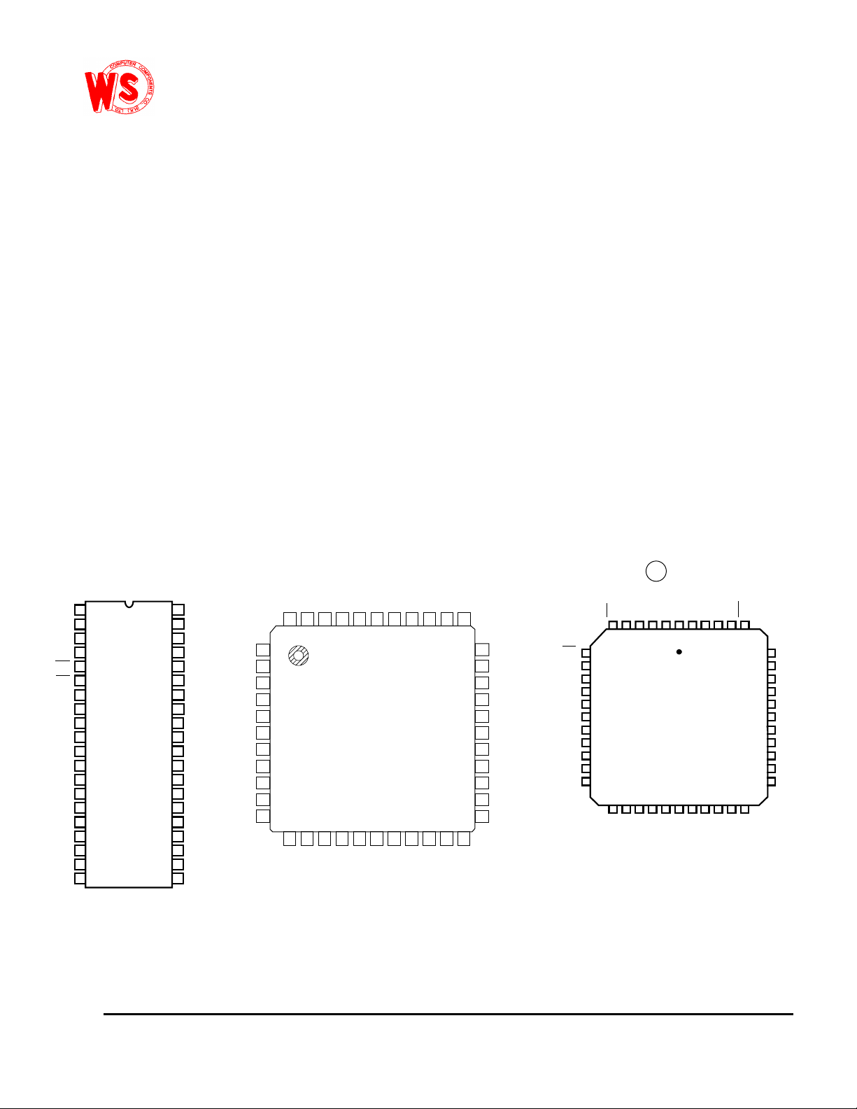
DIP-40
Pinouts
SPEED
QFP-44
44 QFP
44 PLCC
0 C to 70 C
0 C to 70 C
o
o
o
o
PLCC-44
WS82C55A-5P
WS82C55A-5Q
WS82C55A-5C
WS82C55A-5P
WS82C55A-5Q
WS82C55A-5C
0 C to 70 C
o
o
PKG.
TEMPERATURE
RANGE
SPEED
8MHz
8MHz
8MHz
5MHz
5MHz
5MHz
PART NUMBERS
PART NUMBERS
40DIP
Ordering Information
and 8MHz 80C88
The WS82C55A is a high performance CMOS version of
WS82C55A
WS82C55A
WS82C55AP
WS82C55AC
WS82C55AQ
WS82C55AP
WS82C55AQ
WS82C55AC
• Pin Compatible with NMOS 8255A
• 24 Programmable I/O Pins
• Fully TTL Compatible
•HighSpeed,No“WaitState”Operationwith5MHz
• Direct Bit Set/Reset Capability
• Enhanced Control Word Read Capability
• L7 Process
• 2.5mA Drive Capability on All I/O Ports
• Low Standby Power (ICCSB) . . . . . . . . . . . . . . . . .10µA
Description
the industry standard 8255A and is manufactured using a
self-aligned silicon gate CMOS process (Scaled SAJI IV). It
is a general purpose programmableI/Odevice which maybe
used with many different microprocessors. There are 24 I/O
pins which may be individually programmed in 2 groups of
12 and used in 3 major modes of operation. The high
performance and industry standard configuration of the
makeitcompatiblewiththe80C86,and
other microprocessors.
Static CMOS circuit design insures lowoperatingpower. TTL
compatibility over the full military temperature range and bus
hold circuitry eliminate the need for pull-up resistors. The
advancedSAJIprocessresultsinperformanceequal
to or greater than existing functionally equivalent products at
a fraction of the power.
PA3
PA2
PA1
PA0
RD
CS
GND
A1
A0
PC7
PC6
PC5
PC4
PC0
PC1
PC2
PC3
PB0
PB1
PB2
0PA1PA2PA3
RD
1
2
3
4
5
6
7
8
9
10
11
12
13
14
15
16
17
18
19
20
40
PA4
39
PA5
38
PA6
37
PA7
36
WR
35
RESE
34
D0
33
D1
32
D2
31
D3
30
D4
29
D5
28
D6
27
D7
26
V
CC
25
PB7
24
PB6
23
PB5
22
PB4
21
PB3
CS
1
GND
2
A
3
1
A
4
0
PC
5
7
PC
6
6
PC
7
5
PC
8
4
PC
9
0
PC
10
1
PC
11
2
CAUTION: These devices are sensitive to electrostatic discharge; follow proper IC Handling Procedures.
PA
4443424140
1415161718
12
13
3PB0PB1PB2
NC
PC
VCCPA
39
38
CC
V
PB
4
5PA6PA7
PA
37
192021
3
4PB5PB6
PB
363534
WR
22
NC
33
32
31
30
29
28
27
26
25
24
23
RESET
D
0
D
1
D
2.
D
3
D
4
D
5
D
6
D
7
V
CC
PB
7
CS
GND
A1
A0
PC7
NC
PC6
PC5
PC4
PC0
PC1
RD
PA0
7
8
9
10
11
12
13
14
15
16
17
PC2
PC3
PA1
PB0
PA2
PB1
PA3
PB2
NC
PA4
44 43 42 41 40
123456
NC
PB3
PA5
262524232221201918
PB4
PA6
PB5
PA7
PB6
2827
WR
PB7
39
RESET
38
D0
D1
37
D2
36
D3
35
NC
34
D4
33
D5
32
D6
31
D7
30
V
29
CC
Wing Shing Computer Components Co., (H.K.)Ltd. Tel:(852)2341 9276 Fax:(852)2797 8153
Homepage: http://www.wingshing.com E-mail: wsccltd@hkstar.com
1
Pin Description
( For DIP-40)
WS82C55A
PIN
SYMBOL
V
CC
GND 7 GROUND
D0-D7 27-34 I/O DATA BUS: The Data Bus lines are bidirectional three-state pins connected to the
RESET 35 I RESET: A high on this input clears the control register and all ports (A, B, C) are set
CS 6 I CHIP SELECT: Chip select is an active low input used to enable the 82C55A onto the
RD 5 I READ: Read is an active low input control signal used by the CPU to read status
WR 36 I WRITE: Write is an active low input control signal used by the CPU to load control
A0-A1 8, 9 I ADDRESS: These input signals, in conjunction with the RD and WR inputs, control
PA0-PA7 1-4, 37-40 I/O PORT A: 8-bit input and output port. Both bus hold high and bus hold low circuitry are
PB0-PB7 18-25 I/O PORT B: 8-bit input and output port. Bus hold high circuitry is present on this port.
PC0-PC7 10-17 I/O PORT C: 8-bit input and output port. Bus hold circuitry is present on this port.
NUMBER TYPE DESCRIPTION
26 VCC: The +5V power supply pin. A 0.1µF capacitor between pins 26 and 7 is
recommended for decoupling.
system data bus.
to the input mode with the “Bus Hold” circuitry turned on.
Data Bus for CPU communications.
information or data via the data bus.
words and data into the 82C55A.
the selection of one of the three ports or the control word register. A0 and A1 are
normally connected to the least significant bits of the Address Bus A0, A1.
present on this port.
Functional Diagram
POWER
SUPPLIES
BI-DIRECTIONAL
DATA BUS
D7-D0
RD
WR
A1
A0
RESET
+5V
GND
DATA BUS
BUFFER
READ
WRITE
CONTROL
LOGIC
GROUP A
CONTROL
GROUP B
CONTROL
8-BIT
INTERNAL
DATA BUS
GROUP A
PORT A
(8)
GROUP A
PORT C
UPPER
(4)
GROUP B
PORT C
LOWER
(4)
GROUP B
PORT B
(8)
I/O
PA7-PA0
I/O
PC7-PC4
I/O
PC3-PC0
I/O
PB7-PB0
CS
2
Functional Description
and the CPU
82C55A to send
WS82C55A
WS82C55A
WS82C55A
WS82C55A
WS82C55A
trol word to the WS82C55A
WS82C55A
WS
Data Bus Buffer
This three-state bi-directional 8-bit buffer is used to interface
tothesystemdatabus.Dataistransmittedor
received by the buffer upon execution of input or output
instructions by the CPU. Control words and status information are also transferred through the data bus buffer.
Read/Write and Control Logic
The function of this block is to manage all of the internal and
external transfers of both Data and Control or Status words.
It accepts inputs from the CPU Address and Control busses
and in turn, issues commands to both of the Control Groups.
(CS) Chip Select. A “low” on this input pin enables the
communcation between the
(RD)Read.A“low”onthisinputpinenables
the data or status information to the CPU on the data bus. In
essence, it allows the CPU to “read from” the
(WR) Write. A “low” on this input pin enables the CPU to
write data or control words into the
(A0 and A1) Port Select 0 and Port Select 1. These input
signals, in conjunction with the RD and WR inputs, control
the selection of one of the three ports or the control word
register. They are normally connected to the least significant
bits of the address bus (A0 and A1).
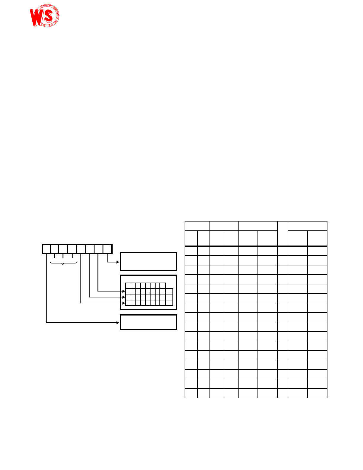
82C55A BASIC OPERATION
INPUT OPERATION
A1 A0 RD WR CS
00010Port A → Data Bus
01010Port B → Data Bus
10010Port C → Data Bus
11010Control Word → Data Bus
00100Data Bus → Port A
01100Data Bus → Port B
(READ)
OUTPUT OPERATION
(WRITE)
I/O
PA7-
POWER
SUPPLIES
BI-DIRECTIONAL
DATA BUS
D7-D0
RD
WR
A1
A0
RESET
CS
FIGURE 1. 82C55A BLOCK DIAGRAM.DATABUSBUFFER,
+5V
GND
DAT A
BUS
BUFFER
READ
WRITE
CONTROL
LOGIC
READ/WRITE, GROUP A & B CONTROL LOGIC
FUNCTIONS
GROUP A
CONTROL
8-BIT
INTERNAL
DATA BUS
GROUP B
CONTROL
GROUP A
PORT A
(8)
GROUP A
PORT C
UPPER
(4)
GROUP B
PORT C
LOWER
(4)
GROUP B
PORT B
(8)
PA0
I/O
PC7-
PC4
I/O
PC3-
PC0
I/O
PB7-
PB0
(RESET) Reset. A “high” on this input initializes the control
register to 9Bh and all ports (A, B, C) are set to the input
mode. “Bus hold” devices internal to the 82C55A will hold
the I/O port inputs to a logic “1” state with a maximum hold
current of 400µA.
Group A and Group B Controls
The functional configuration of each port is programmed by
the systems software. In essence, the CPU “outputs” a con-
.Thecontrolwordcontains
information such as “mode”, “bit set”, “bit reset”, etc., that initializes the functional configuration of the
Each of the Control blocks (Group A and Group B) accepts
“commands” from the Read/Write Control logic, receives
“control words” from the internal data bus and issues the
proper commands to its associated ports.
Control Group A - Port A and Port C upper (C7 - C4)
Control Group B - Port B and Port C lower (C3 - C0)
The control word register can be both written and read as
shown in the “Basic Operation” table. Figure 4 shows the
control word format for both Read and Write operations.
When the control word is read, bit D7 will always be a logic
“1”, as this implies control word mode information.
10100Data Bus → Port C
11100Data Bus → Control
XXXX1Data Bus → Three-State
X X 1 1 0 Data Bus → Three-State
DISABLE FUNCTION
3
Ports A, B, and C
WS82C55A
The WS82C55A
WS82C55A
WS82C55A
containsthree8-bitports(A,B,andC).Allcan
be configured to a wide variety of functional characteristics
by the system software but each has its own special features
or “personality” to further enhance the power and flexibility of
the
Port A One 8-bit data output latch/buffer and one 8-bit data
input latch. Both “pull-up” and “pull-down” bus-hold devices
are present on Port A. See Figure 2A.
Port B One 8-bit data input/output latch/buffer and one 8-bit
data input buffer. See Figure 2B.
register will contain 9Bh. During the execution of the system
program, any of the other modes may be selected using a
single output instruction. This allows a single 82C55A to
service a variety of peripheral devices with a simple software
maintenance routine. Any port programmed as an output
port is initialized to all zeros when the control word is written.
ADDRESS BUS
CONTROL BUS
DATA BUS
Port C One 8-bit data output latch/buffer and one 8-bit data
input buffer (no latch for input). This port can be divided into
two 4-bit ports under the mode control. Each 4-bit port contains a 4-bit latch and it can be used for the control signal
output and status signal inputs in conjunction with ports A
and B. See Figure 2B.
MASTER
RESET
OR MODE
CHANGE
INTERNAL
DATA IN
INTERNAL
DATA OUT
(LATCHED)
FIGURE 2A. PORT A BUS-HOLD CONFIGURATION
RESET
OR MODE
CHANGE
INTERNAL
DATA IN
INTERNAL
DATA OUT
(LATCHED)
FIGURE 2B. PORT B AND C BUS-HOLD CONFIGURATION
FIGURE 2. BUS-HOLD CONFIGURATION
INPUT MODE
OUTPUT MODE
OUTPUT MODE
V
CC
P
EXTERNAL
PORT A PIN
EXTERNAL
PORT B, C
PIN
Operational Description
Mode Selection
There are three basic modes of operation than can be
selected by the system software:
Mode 0 - Basic Input/Output
Mode 1 - Strobed Input/Output
Mode 2 - Bi-directional Bus
When the reset input goes “high”, all ports will be set to the
input mode with all 24 port lines held at a logic “one” level by
internal bus hold devices. After the reset is removed, the
canremainintheinputmodewithnoadditionalinitialization required. This eliminates the need to pullup or pulldown resistors in all-CMOS designs. The control word
D7-D0 A0-A1
82C55A
C
4 I/O
PC3-PC0
OR I/O
PC7-PC4
C
CONTROL
OR I/O
C
CONTROL
4 I/O
CS
A
8 I/O
PA7-PA0
A
8 I/O
PA7-PA0
A
BIDIRECTIONAL
PA7-PA0
MODE 0
MODE 1
MODE 2
RD, WR
B
8 I/O
PB7-PB0
B
8 I/O
PB7-PB0 CONTROL
B
8 I/O
PB7-PB0
FIGURE 3. BASIC MODE DEFINITIONS AND BUS INTERFACE
CONTROL WORD
D7 D6 D5 D4 D3 D2 D1 D0
GROUP B
PORT C (LOWER)
1 = INPUT
0 = OUTPUT
PORT B
1 = INPUT
0 = OUTPUT
MODE SELECTION
0 = MODE 0
1 = MODE 1
GROUP A
PORT C (UPPER)
1 = INPUT
0 = OUTPUT
PORT A
1 = INPUT
0 = OUTPUT
MODE SELECTION
00 = MODE 0
01 = MODE 1
1X = MODE 2
MODE SET FLAG
1 = ACTIVE
FIGURE 4. MODE DEFINITION FORMAT
4
The modes for Port A and Port B can be separately defined,
WS82C55A
When WS82C55A
while Port C is divided into two portions as required by the
Port A and Port B definitions. All of the output registers,
including the status flip-flops, will be reset whenever the
mode is changed. Modes may be combined so that their
functional definition can be “tailored” to almost any I/O
structure. For instance: Group B can be programmed in
Mode 0 to monitor simple switch closings or display computational results, Group A could be programmed in Mode 1 to
monitor a keyboard or tape reader on an interrupt-driven
basis.
This function allows the programmer to enable or disable a
CPU interrupt by a specific I/O device without affecting any
other device in the interrupt structure.
INTE Flip-Flop Definition
(BIT-SET)-INTE is SET - Interrupt Enable
(BIT-RESET)-INTE is Reset - Interrupt Disable
NOTE: All Mask flip-flops are automatically reset during mode selection and device Reset.
The mode definitions and possible mode combinations may
seem confusing at first, but after a cursory review of the
complete device operation a simple, logical I/O approach will
surface. The design of the 82C55A has taken into account
things such as efficient PC board layout, control signal definition vs. PC layout and complete functional flexibility to support almost any peripheral device with no external logic.
Such design represents the maximum use of the available
pins.
Single Bit Set/Reset Feature (Figure 5)
Any of the eight bits of Port C can be Set or Reset using a
single Output instruction. This feature reduces software
requirements in control-based applications.
When Port C is being used as status/control for Port A or B,
these bits can be set or reset by using the Bit Set/Reset
operation just as if they were output ports.
CONTROL WORD
D7 D6 D5 D4 D3 D2 D1 D0
XXX
DON’T
CARE
FIGURE 5. BIT SET/RESET FORMAT
BIT SET/RESET
1 = SET
0 = RESET
BIT SELECT
0
1234567
01010101
00110011
00001111
BIT SET/RESET FLAG
0 = ACTIVE
B0
B1
B2
Interrupt Control Functions
isprogrammedtooperateinmode1or
mode 2, control signals are provided that can be used as
interrupt request inputs to the CPU. The interrupt request
signals, generated from port C, can be inhibited or enabled
by setting or resetting the associated INTE flip-flop, using the
bit set/reset function of port C.
Operating Modes
Mode 0 (Basic Input/Output). This functional configuration
provides simple input and output operations for each of the
three ports. No handshaking is required, data is simply written to or read from a specific port.
Mode 0 Basic Functional Definitions:
• Two 8-bit ports and two 4-bit ports
• Any Port can be input or output
• Outputs are latched
• Input are not latched
• 16 different Input/Output configurations possible
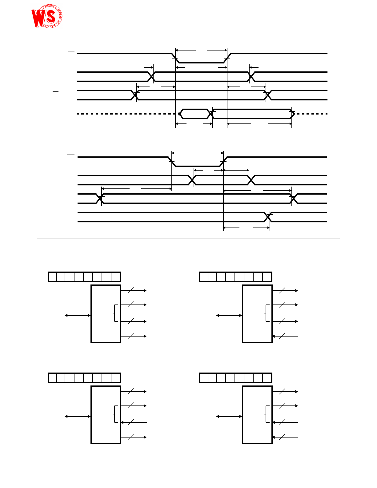
MODE 0 PORT DEFINITION
A B GROUP A
PORTC
D4 D3 D1 D0 PORTA
0 0 0 0 Output Output 0 Output Output
0 0 0 1 Output Output 1 Output Input
0 0 1 0 Output Output 2 Input Output
0 0 1 1 Output Output 3 Input Input
0 1 0 0 Output Input 4 Output Output
0 1 0 1 Output Input 5 Output Input
0 1 1 0 Output Input 6 Input Output
0 1 1 1 Output Input 7 Input Input
1 0 0 0 Input Output 8 Output Output
1 0 0 1 Input Output 9 Output Input
1 0 1 0 Input Output 10 Input Output
1 0 1 1 Input Output 11 Input Input
1 1 0 0 Input Input 12 Output Output
1 1 0 1 Input Input 13 Output Input
1 1 1 0 Input Input 14 Input Output
1 1 1 1 Input Input 15 Input Input
(Upper) PORT B
#
GROUP B
PORTC
(Lower)
5
Mode 0 (Basic Input)
WS82C55A
RD
tRR
INPUT
CS, A1, A0
D7-D0
Mode 0 (Basic Output)
WR
D7-D0
CS, A1, A0
OUTPUT
Mode 0 Configurations
tAW
tAR
tIR
tHR
tRA
tRD tDF
tWW
tDW
tWD
tWA
tWB
CONTROL WORD #0 CONTROL WORD #2
82C55A
C
D0
1D70D60D50D40D30D21D10
8
4
4
8
PA7 - PA0
PC7 - PC4
D7 - D0
PC3 - PC0
PB7 - PB0
A
B
D7
0D60D50D40D30D20D10
1
D7 - D0
CONTROL WORD #1 CONTROL WORD #3
D0
1D70D60D50D40D30D20D11
82C55A
D7 - D0
8
4
4
8
PA7 - PA0
PC7 - PC4
PC3 - PC0
PB7 - PB0
A
C
B
1D70D60D50D40D30D21D11
D7 - D0
82C55A
C
82C55A
C
D0
D0
8
4
4
8
8
4
4
8
PA7 - PA0
PC7 - PC4
PC3 - PC0
PB7 - PB0
PA7 - PA0
PC7 - PC4
PC3 - PC0
PB7 - PB0
A
B
A
B
6
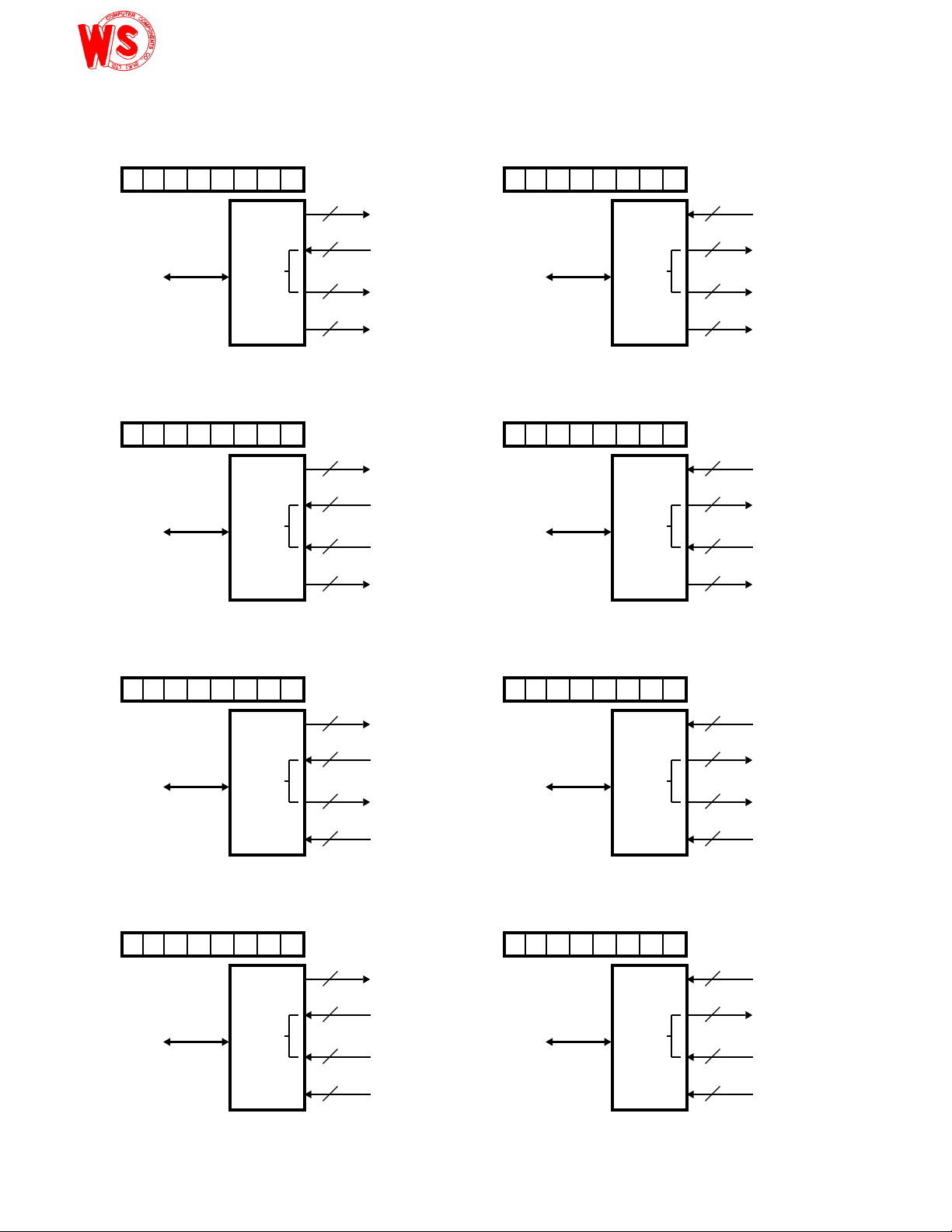
Mode 0 Configurations (Continued)
WS82C55A
CONTROL WORD #4 CONTROL WORD #8
D0
1D70D60D50D41D30D20D10
82C55A
D7 - D0
8
4
4
PA7 - PA0
PC7 - PC4
PC3 - PC0
A
C
1D70D60D51D40D30D20D10
D7 - D0
82C55A
C
D0
8
4
4
PA7 - PA0
PC7 - PC4
PC3 - PC0
A
8
B
PB7 - PB0
CONTROL WORD #5 CONTROL WORD #9
D0
1D70D60D50D41D30D20D11
82C55A
D7 - D0
8
4
4
8
PA7 - PA0
PC7 - PC4
PC3 - PC0
PB7 - PB0
A
C
B
1D70D60D51D40D30D20D11
D7 - D0
CONTROL WORD #6 CONTROL WORD #10
D0
1D70D60D50D41D30D21D10
82C55A
D7 - D0
8
4
4
PA7 - PA0
PC7 - PC4
PC3 - PC0
A
C
1D70D60D51D40D30D21D10
D7 - D0
82C55A
C
82C55A
C
D0
D0
8
8
4
4
8
8
4
4
PB7 - PB0
PA7 - PA0
PC7 - PC4
PC3 - PC0
PB7 - PB0
PA7 - PA0
PC7 - PC4
PC3 - PC0
B
A
B
A
8
B
PB7 - PB0
CONTROL WORD #7 CONTROL WORD #11
D0
1D70D60D50D41D30D21D11
82C55A
D7 - D0
8
4
4
8
PA7 - PA0
PC7 - PC4
PC3 - PC0
PB7 - PB0
A
C
B
1D70D60D51D40D30D21D11
D7 - D0
7
82C55A
C
D0
8
8
4
4
8
PB7 - PB0
PA7 - PA0
PC7 - PC4
PC3 - PC0
PB7 - PB0
B
A
B
Mode 0 Configurations (Continued)
WS82C55A
CONTROL WORD #12 CONTROL WORD #14
D0
1D70D60D51D41D30D20D10
82C55A
D7 - D0
8
4
4
PA7 - PA0
PC7 - PC4
PC3 - PC0
A
C
1D70D60D51D41D30D21D10
D7 - D0
82C55A
C
D0
8
4
4
PA7 - PA0
PC7 - PC4
PC3 - PC0
A
8
B
PB7 - PB0
CONTROL WORD #13 CONTROL WORD #15
D0
1D70D60D51D41D30D20D11
82C55A
D7 - D0
8
4
4
8
PA7 - PA0
PC7 - PC4
PC3 - PC0
PB7 - PB0
A
C
B
1D70D60D51D41D30D21D11
D7 - D0
Operating Modes
Mode 1 - (Strobed Input/Output). This functional configura-
tion provides a means for transferring I/O data to or from a
specified port in conjunction with strobes or “hand shaking”
signals. In mode 1, port A and port B use the lines on port C
to generate or accept these “hand shaking” signals.
Mode 1 Basic Function Definitions:
• Two Groups (Group A and Group B)
• Each group contains one 8-bit port and one 4-bit
control/data port
• The 8-bit data port can be either input or output. Both
inputs and outputs are latched.
• The 4-bit port is used for control and status of the 8-bit
port.
Input Control Signal Definition
(Figures 6 and 7)
CONTROL WORD
1D70D61D51D41/0
CONTROL WORD
D6 D5 D4 D3 D2 D1 D0
D7
1
D3
82C55A
D2 D1 D0
PC6, PC7
1 = INPUT
0 = OUTPUT
RD
11
B
D0
A
C
B
8
PB7 - PB0
8
PA7 - PA0
4
PC7 - PC4
4
PC3 - PC0
8
PB7 - PB0
MODE 1 (PORT A)
PA7-PA0
INTE
A
MODE 1 (PORT B)
INTE
B
PC4
PC3
PC6, PC7
PB7-PB0
PC2
2
8
STBA
IBFAPC5
INTRA
I/O
8
STBB
IBFBPC1
STB (Strobe Input)
A “low” on this input loads data into the input latch.
IBF (Input Buffer Full F/F)
A “high” on this output indicates that the data has been
loaded into the input latch: in essence, and acknowledgment. IBF is set by
rising edge of the
STB input being low and is reset by the
RD input.
PC0
RD
INTRB
FIGURE 6. MODE 1 INPUT
8

STB
WS82C55A
tST
IBF
INTR
RD
INPUT FROM
PERIPHERAL
tSIB
tSIT
tPH
tPS
FIGURE 7. MODE 1 (STROBED INPUT)
INTR (Interrupt Request)
A “high” on this output can be used to interrupt the CPU
when and input device is requesting service. INTR is set by
the condition:
“one”. It is reset by the falling edge of
STB is a “one”, IBF is a “one” and INTE is a
RD. This procedure
allows an input device to request service from the CPU by
simply strobing its data into the port.
INTE A
Controlled by bit set/reset of PC4.
INTE B
Controlled by bit set/reset of PC2.
Output Control Signal Definition
(Figure 8 and 9)
OBF - Output Buffer Full F/F). The OBF output will go “low”
to indicate that the CPU has written data out to be specified
port. This does not mean valid data is sent out of the part at
this time since
Data is guaranteed valid at the rising edge of
Note 1). The
OBF can go true before data is available.
OBF, (See
OBF F/F will be set by the rising edge of the
WR input and reset by ACK input being low.
ACK - Acknowledge Input). A “low” on this input informs the
82C55A that the data from Port A or Port B is ready to be
accepted. In essence, a response from the peripheral device
indicating that it is ready to accept data, (See Note 1).
INTR - (Interrupt Request). A “high” on this output can be
used to interrupt the CPU when an output device has
accepted data transmitted by the CPU. INTR is set when
ACK is a “one”, OBF is a “one” and INTE is a “one”. It is
reset by the falling edge of
WR.
tRIB
tRIT
INTE A
Controlled by Bit Set/Reset of PC6.
INTE B
Controlled by Bit Set/Reset of PC2.
NOTE:
1. To strobe data into the peripheral device, the user must operate
the strobe line in a hand shaking mode. The user needs to send
OBF to the peripheral device, generates an ACK from the peripheral device and then latch data into the peripheral device on
the rising edge of OBF.
MODE 1 (PORT A)
PC7
PC3
PC1
PC0
8
OBFA
ACKAPC6
INTRA
2
8
OBFB
ACKBPC2
INTRB
CONTROL WORD
1D70D61D51D41/0
CONTROL WORD
D6 D5 D4 D3 D2 D1 D0
D7
1
D2 D1 D0
D3
10
PC4, PC5
1 = INPUT
0 = OUTPUT
WR
WR
PA7-PA0
INTE
A
PC4, PC5
MODE 1 (PORT B)
PB7-PB0
INTE
B
FIGURE 8. MODE 1 OUTPUT
9

WR
WS82C55A
tWOB
OBF
INTR
ACK
OUTPUT
CONTROL WORD
1D70D61D51D41/0
tWIT
FIGURE 9. MODE 1 (STROBED OUTPUT)
PC4
PC5
PC3
PC1
PC2
PC0
8
2
8
STBA
IIBFA
INTRA
I/O
OBFB
ACKB
INTRB
PA7-PA0
RD
D2 D1 D0
D3
10 1
PC6, PC7
1 = INPUT
0 = OUTPUT
WR
PC6, PC7
PB7, PB0
tWB
CONTROL WORD
D7
0D61D50D41/0
tAOB
tAK tAIT
WR
D2 D1 D0
D3
11
PC4, PC5
1 = INPUT
0 = OUTPUT
RD
PA7-PA0
PC7
PC6
PC3
PC4, PC5
PB7, PB0
PC2
PC1
PC0
8
2
8
OBFA
ACKA
INTRA
I/O
STBB
IBFB
INTRB
PORT A - (STROBED INPUT)
PORT B - (STROBED OUTPUT)
PORT A - (STROBED OUTPUT)
PORT B - (STROBED INPUT)
Combinations of Mode 1: Port A and Port B can be individually defined as input or output in Mode 1 to support a wide variety of strobed I/O
applications.
FIGURE 10. COMBINATIONS OF MODE 1
Operating Modes
Mode 2 (Strobed Bi-Directional Bus I/O)
The functional configuration provides a means for communicating with a peripheral device or structure on a single 8-bit
bus for both transmitting and receiving data (bi-directional
bus I/O). “Hand shaking” signals are provided to maintain
proper bus flow discipline similar to Mode 1. Interrupt generation and enable/disable functions are also available.
Mode 2 Basic Functional Definitions:
• Used in Group A only
• One 8-bit, bi-directional bus Port (Port A) and a 5-bit
control Port (Port C)
• Both inputs and outputs are latched
• The 5-bit control port (Port C) is used for control and
status for the 8-bit, bi-directional bus port (Port A)
Bi-Directional Bus I/O Control Signal Definition
(Figures 11, 12, 13, 14)
INTR - (Interrupt Request). A high on this output can be
used to interrupt the CPU for both input or output operations.
Output Operations
OBF - (Output Buffer Full). The OBF output will go “low” to
indicate that the CPU has written data out to port A.
ACK - (Acknowledge). A “low” on this input enables the
three-state output buffer of port A to send out the data. Otherwise, the output buffer will be in the high impedance state.
INTE 1 - (The INTE flip-flop associated with
OBF). Con-
trolled by bit set/reset of PC4.
Input Operations
STB - (Strobe Input). A “low” on this input loads data into the
input latch.
IBF - (Input Buffer Full F/F). A “high” on this output indicates
that data has been loaded into the input latch.
INTE 2 - (The INTE flip-flop associated with IBF). Controlled
by bit set/reset of PC4.
10

CONTROL WORD
WS82C55A
WS82C55A
WS82C55A
WS82C55A
D6 D5 D4 D3 D2 D1 D0
D7
1
1/0 1/01 1/0
PC3
PA7-PA0
INTRA
8
PC2-PC0
1 = INPUT
0 = OUTPUT
PORT B
1 = INPUT
0 = OUTPUT
GROUP B MODE
0 = MODE 0
1 = MODE 1
WR
RD
FIGURE 11. MODE CONTROL WORD FIGURE 12. MODE 2
DATA FROM
CPU TO 82C55A
WR
tAOB
OBF
tWOB
INTR
tAK
ACK
INTE
1
INTE
2
PC7
PC6
PC4
PC5
PC2-PC0
3
OBFA
ACKA
STBA
IBFA
I/O
PERIPHERAL
NOTE: Any sequence where WR occurs before ACK and STB occurs before RD is permissible. (INTR = IBF • MASK • STB • RD ÷ OBF •
STB
IBF
BUS
RD
MASK • ACK • WR)
tST
tSIB
tPS
tPH
DATA FROM
PERIPHERAL TO
FIGURE 13. MODE 2 (BI-DIRECTIONAL)
11
tAD
DATA FROM
TO PERIPHERAL
tKD
tRIB
DATA FROM
TO CPU

MODE 2 AND MODE 0 (INPUT) MODE 2 AND MODE 0 (OUTPUT)
WS82C55A
CONTROL WORD
D5 D4 D3 D2 D1 D0
D6
1D71
01
PC2-PC0
1 = INPUT
0 = OUTPUT
RD
WR
1/0
PC3
PA7-PA0
PC7
PC6
PC4
PC5
PC2-PC0
PB7-PB0
8
3
8
INTRA
OBFA
ACKA
STBA
IBFA
I/O
CONTROL WORD
D5 D4 D3 D2 D1 D0
D7
D6
1
1
00
PC2-PC0
1 = INPUT
0 = OUTPUT
RD
WR
1/0
MODE 2 AND MODE 1 (OUTPUT) MODE 2 AND MODE 1 (INPUT)
CONTROL WORD
D5 D4 D3 D2 D1 D0
D6
D7
1
1
10
PC3
PA7-PA0
PC7
PC6
PC4
PC5
PB7-PB0
8
8
INTRA
OBFA
ACKA
STBA
IBFA
CONTROL WORD
D7
D5 D4 D3 D2 D1 D0
D6
1
1
11
PC3
PA7-PA0
PC7
PC6
PC4
PC5
PC2-PC0
PB7, PB0
PC3
PA7-PA0
PC7
PC6
PC4
PC5
PB7-PB0
8
3
8
8
8
INTRA
OBFA
ACKA
STBA
IBFA
I/O
INTRA
OBFA
ACKA
STBA
IBFA
RD
WR
PC1
PC2
PC0
OBFB
ACKB
INTRB
FIGURE 14. MODE 2 COMBINATIONS
RD
WR
PC2
PC1
PC0
STBB
IBFB
INTRB
12

PA0
WS82C55A
PA1
PA2
PA3
PA4
PA5
PA6
PA7
PB0
PB1
PB2
PB3
PB4
PB5
PB6
PB7
PC0
PC1
PC2
PC3
PC4
PC5
PC6
PC7
MODE DEFINITION SUMMARY
MODE 0 MODE 1 MODE 2
IN OUT IN OUT GROUP A ONLY
In
In
In
In
In
In
In
In
In
In
In
In
In
In
In
In
In
In
In
In
In
In
In
In
Out
Out
Out
Out
Out
Out
Out
Out
Out
Out
Out
Out
Out
Out
Out
Out
Out
Out
Out
Out
Out
Out
Out
Out
In
In
In
In
In
In
In
In
In
In
In
In
In
In
In
In
INTRB
IBFB
STBB
INTRA
STBA
IBFA
I/O
I/O
Out
Out
Out
Out
Out
Out
Out
Out
Out
Out
Out
Out
Out
Out
Out
Out
INTRB
OBFB
ACKB
INTRA
I/O
I/O
ACKA
OBFA
I/O
I/O
I/O
INTRA
STBA
IBFA
ACKA
OBFA
Mode 0
or Mode 1
Only
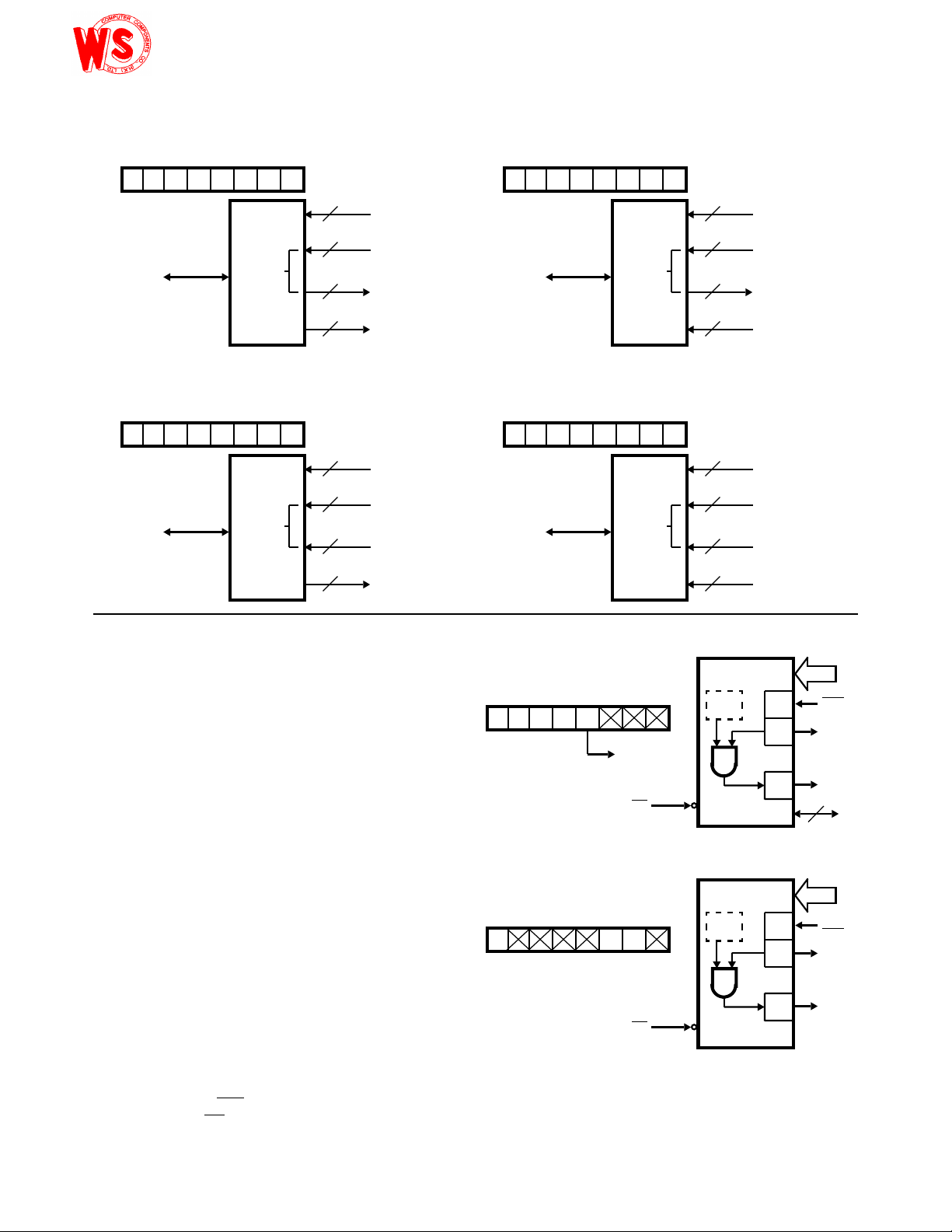
Special Mode Combination Considerations
There are several combinations of modes possible. For any
combination, some or all of Port C lines are used for control
or status. The remaining bits are either inputs or outputs as
defined by a “Set Mode” command.
During a read of Port C, the state of all the Port C lines,
except the
bus. In place of the
ACK and STB lines, will be placed on the data
ACK and STB line states, flag status will
appear on the data bus in the PC2, PC4, and PC6 bit
positions as illustrated by Figure 17.
Through a “Write Port C” command, only the Port C pins
programmed as outputs in a Mode 0 group can be written.
No other pins can be affected by a “Write Port C” command,
nor can the interrupt enable flags be accessed. To write to
any Port C output programmed as an output in Mode 1 group
or to change an interrupt enable flag, the “Set/Reset Port C
Bit” command must be used.
With a “Set/Reset Port Cea Bit” command, any Port C line
programmed as an output (including IBF and
OBF) can be
written, or an interrupt enable flag can be either set or reset.
Port C lines programmed as inputs, including
ACK and STB
lines, associated with Port C fare not affected by a
“Set/Reset Port C Bit” command. Writing to the corresponding Port C bit positions of the
ACK and STB lines with the
“Set Reset Port C Bit” command will affect the Group A and
Group B interrupt enable flags, as illustrated in Figure 17.
INPUT CONFIGURATION
D7 D6 D5 D4 D3 D2 D1 D0
I/O I/O IBFA INTEA INTRA INTEB IBFB INTRB
GROUP A
OUTPUT CONFIGURATION
D7 D6 D5 D4 D3 D2 D1 D0
OBFA INTEA I/O I/O INTRA INTEB OBFB INTRB
GROUP A
FIGURE 15. MODE 1 STATUS WORD FORMAT
D7 D6 D5 D4 D3 D2 D1 D0
OBFA INTE1 IBFA INTE2 INTRA X X X
GROUP A
(Defined by Mode 0 or Mode 1 Selection)
FIGURE 16. MODE 2 STATUS WORD FORMAT
GROUP B
GROUP B
GROUP B
Current Drive Capability
Any output on Port A, B or C can sink or source 2.5mA. This
feature allows the 82C55A to directly drive Darlington type
drivers and high-voltage displays that require such sink or
source current.
13

Reading Port C Status (Figures 15 and 16)
WS82C55A-5
WS82C55A
WS82C55A
WS82C55A
WS82C55A to exactly "fit" the
the WS82C55A is programmed
In Mode 0, Port C transfers data to or from the peripheral
device.Whenthe82C55Aisprogrammedtofunctionin
Modes 1 or 2, Port C generates or accepts “hand shaking”
signals with the peripheral device. Reading the contents of
Port C allows the programmer to test or verify the “status” of
each peripheral device and change the program flow
accordingly.
There is not special instruction to read the status information
from Port C. A normal read operation of Port C is executedto
perform this function.
INTERRUPT
ENABLE FLAG POSITION
INTE B PC2 ACKB (Output Mode 1)
INTE A2 PC4 STBA (Input Mode 1 or
INTE A1 PC6 ACKA (Output Mode 1 or
FIGURE 17. INTERRUPT ENABLE FLAGS IN MODES 1 AND 2
ALTERNATE PORT C
PIN SIGNAL (MODE)
or STBB (Input Mode 1)
Mode 2)
Mode 2)
INTERRUPT
REQUEST
PC3
MODE 1
(OUTPUT)
82C55A
MODE 1
(OUTPUT)
PC0
INTERRUPT
REQUEST
PA0
PA1
PA2
PA3
PA4
PA5
PA6
PA7
PC7
PC6
PC5
PC4
PB0
PB1
PB2
PB3
PB4
PB5
PB6
PB7
PC1
PC2
CONTROL LOGIC
Applications of the
isaverypowerfultoolforinterfacingperipheral
equipment to the microcomputer system. It represents the
optimum use of available pins and flexible enough to interface almost any I/O device without the need for additional
external logic.
Each peripheral device in a microcomputer system usually
has a “service routine” associated with it. The routine
manages the software interface between the device and the
CPU.Thefunctionaldefinitionof
by the I/O service routine and becomes an extension of the
system software. By examining the I/O devices interface
characteristics for both data transfer and timing, and
matching this information to the examples and tables in the
detailed operational description, a control word can easily be
developedtoinitializethe
application. Figures 18 through 24 present a few examples
of typical applications of the
HIGH SPEED
PRINTER
HAMMER
RELAYS
DATA READY
ACK
PAPER FEED
FORWARD/REV.
PAPER FEED
FORWARD/REV.
RIBBON
CARRIAGE SEN.
DATA READY
ACK
AND DRIVERS
FIGURE 18. PRINTER INTERFACE
14

INTERRUPT
WS82C55A-5
WS82C55A-5
WS
82C55A-5
WS82C55A-5
WS82C55A
REQUEST
R0
R1
R2
R3
R4
R5
SHIFT
CONTROL
STROBE
ACK
B0
B1
B2
B3
B4
B5
BACKSPACE
CLEAR
DATA READY
ACK
BLANKING
CANCEL WORD
FULLY
DECODED
KEYBOARD
BURROUGHS
SELF-SCAN
DISPLAY
INTERRUPT
REQUEST
PC3
MODE 1
(INPUT)
MODE 1
(OUTPUT)
PA0
PA1
PA2
PA3
PA4
PA5
PA6
PA7
PC4
PC5
PB0
PB1
PB2
PB3
PB4
PB5
PB6
PB7
PC1
PC2
PC6
PC7
FIGURE 19. KEYBOARD AND DISPLAY INTERFACE
INTERRUPT
REQUEST
PC3
MODE 1
(INPUT)
MODE 0
(INPUT)
PA0
PA1
PA2
PA3
PA4
PA5
PA6
PA7
PC4
PC5
PC6
PC7
PB0
PB1
PB2
PB3
PB4
PB5
PB6
PB7
R0
R1
R2
R3
R4
KEYBOARD
R5
SHIFT
CONTROL
STROBE
ACK
BUST LT
TEST LT
FULLY
DECODED
TERMINAL
ADDRESS
FIGURE 20. KEYBOARDANDTERMINAL ADDRESS
INTERFACE
MODE 0
(OUTPUT)
BIT
SET/RESET
MODE 0
(INPUT)
PA0
PA1
PA2
PA3
PA4
PA5
PA6
PA7
PC4
PC5
PC6
PC7
PC0
PC1
PC2
PC3
PB0
PB1
PB2
PB3
PC4
PC5
PC6
PC7
LSB
12-BIT
A/D
CONVERTER
(DAC)
STB DATA
SAMPLE EN
STB
LSB
8-BIT
D/A
CONVERTER
(ADC)
MAB
ANALOG
OUTPUT
ANALOG
INPUT
INTERRUPT
REQUEST
PC3
MODE 1
(OUTPUT)
MODE 0
(OUTPUT)
PA0
PA1
PA2
PA3
PA4
PA5
PA6
PA7
PC7
PC6
PC5
PC4
PC2
PC1
PC0
PB0
PB1
PB2
PB3
PB4
PB5
PB6
PB7
R0
R1
R2
CRT CONTROLLER
R3
• CHARACTER GEN.
• REFRESH BUFFER
R4
• CURSOR CONTROL
R5
SHIFT
CONTROL
DATA READY
ACK
BLANKED
BLACK/WHITE
ROW STB
COLUMN STB
CURSOR H/V STB
CURSOR/ROW/COLUMN
ADDRESS
H&V
FIGURE 21. DIGITAL TO ANALOG, ANALOG TO DIGITAL FIGURE 22. BASIC CRT CONTROLLER INTERFACE
15

INTERRUPT
WS82C55A-5
WS82C55A-5
WS82C55A
REQUEST
PC3
MODE 2
PA0
PA1
PA2
PA3
PA4
PA5
PA6
PA7
D0
D1
D2
D3
D4
D5
D6
D7
FLOPPY DISK
CONTROLLER
AND DRIVE
INTERRUPT
REQUEST
PC3
MODE 1
(INPUT)
PA0
PA1
PA2
PA3
PA4
PA5
PA6
PA7
R0
R1
R2
R3
R4
R5
R6
R7
B LEVEL
PAPER
TAPE
READER
MODE 0
(OUTPUT)
PC4
PC5
PC7
PC6
PC2
PC1
PC0
PB0
PB1
PB2
PB3
PB4
PB5
PB6
PB7
DATA STB
ACK (IN)
DATA READY
ACK (OUT)
TRACK “0” SENSOR
SYNC READY
INDEX
ENGAGE HEAD
FORWARD/REV.
READ ENABLE
WRITE ENABLE
DISC SELECT
ENABLE CRC
TEST
BUSY LT
MODE 0
(INPUT)
MODE 0
(OUTPUT)
PC4
PC5
PC6
PC0
PC1
PC2
PB0
PB1
PB2
PB3
PB4
PB5
PB6
PB7
STB
ACK
STOP/GO
MACHINE TOOL
START/STOP
LIMIT SENSOR (H/V)
OUT OF FLUID
CHANGE TOOL
LEFT/RIGHT
UP/DOWN
HOR. STEP STROBE
VERT. STEP STROBE
SLEW/STEP
FLUID ENABLE
EMERGENCY STOP
FIGURE 23. BASIC FLOPPY DISC INTERFACE FIGURE 24. MACHINE TOOL CONTROLLER INTERFACE
16

Absolute Maximum Ratings T
WS82C55A-5);
WS82C55A
WS82C55A
Supply Voltage . . . . . . . . . . . . . . . . . . . . . . . . . . . . . . . . . . . . .+8.0V
Input, Output or I/O Voltage . . . . . . . . . . . . GND-0.5V to VCC+0.5V
ESD Classification . . . . . . . . . . . . . . . . . . . . . . . . . . . . . . . . Class 1
= 25oC Thermal Information
A
Thermal Resistance (Typical, Note 1) θ
PDIP Package. . . . . . . . . . . . . . . . . . . 50oC/W N/A
JA
θ
JC
Operating Conditions
Voltage Range . . . . . . . . . . . . . . . . . . . . . . . . . . . . . . +4.5V to 5.5V
Operating Temperature Range
. . . . . . . . . . . . . . . . . . . . . . . . . . . . . . . . . .0oC to 70oC
Maximum Storage Temperature Range . . . . . . . . . .-65oC to 150oC
Maximum Junction Temperature
PDIP Package. . . . . . . . . . . . . . . . . . . . . . . . . . . . . . . . . . . 150oC
Die Characteristics
Gate Count . . . . . . . . . . . . . . . . . . . . . . . . . . . . . . . . . . .1000 Gates
CAUTION: Stresses above those listed in “Absolute Maximum Ratings” may cause permanent damage to the device. This is a stress only rating and operation
of the device at these or any other conditions above those indicated in the operational sections of this specification is not implied.
NOTE:
1. θJA is measured with the component mounted on an evaluation PC board in free air.
Electrical Specifications V
SYMBOL PARAMETER
V
V
V
OH
V
OL
IO I/O Pin Leakage Current -10 +10 µA VO = VCC or GND DIP Pins: 27 - 34
IBHH Bus Hold High Current -50 -400 µA VO = 3.0V. Ports A, B, C
IBHL Bus Hold Low Current 50 400 µA VO = 1.0V. Port A ONLY
IDAR Darlington Drive Current -2.5 Note 2, 4 mA Ports A, B, C. Test Condition 3
ICCSB Standby Power Supply Current - 10 µAVCC = 5.5V, VIN = VCC or GND. Output Open
ICCOP Operating Power Supply Current - 1 mA/MHz TA = +25oC, VCC = 5.0V, Typical (See Note 3)
NOTES:
2. No internal current limiting exists on Port Outputs. A resistor must be added externally to limit the current.
3. ICCOP = 1mA/MHz of Peripheral Read/Write cycle time. (Example: 1.0µs I/O Read/Write cycle time = 1mA).
4. Tested as VOH at -2.5mA.
Logical One Input Voltage 2.0
IH
Logical Zero Input Voltage - 0.8 V
IL
Logical One Output Voltage 3.0
Logical Zero Output Voltage - 0.4 V IOL +2.5mA
I
Input Leakage Current -1.0 +1.0 µAVIN = VCC or GND,
I
= 5.0V±10%; TA = 0oC to +70oC (
CC
LIMITS
2.2
VCC -0.4
UNITS TEST CONDITIONSMIN MAX
-V
-VI
= -2.5mA,
OH
IOH = -100µA
DIP Pins: 5, 6, 8, 9, 35, 36
Capacitance T
= 25oC
A
SYMBOL PARAMETER TYPICAL UNITS TEST CONDITIONS
CIN Input Capacitance 10 pF FREQ = 1MHz, All Measurements are
CI/O I/O Capacitance 20 pF
referenced to device GND
17

AC Electrical Specifications V
o
o
0 C
to 70 C
ns
ns
nsnsns
ns
12nsnsns
nsnsnsns1
nsnsnsnsns
nsnsnsnsnsnsns
ns
nsnsns
1
2
1111111
1
1,(Note)
WS82C55A
WS82C55A*5
WS-XX82C55A
MIN
MAX
0--0150-120-1075300-020--100
100-30---35000--
200-100-20-50--
17520250-150-150-150-150
-
200-150-150-200
500
-
SYMBOL PARAMETER UNITS
READ TIMING
= +5V± 10%, GND = 0V; TA =
CC
TEST
CONDITIONSMINMAX
(1) tAR Address Stable Before
(2) tRA Address Stable After
(3) tRR
(4) tRD Data Valid From
(5) tDF Data Float After
(6) tRV Time Between
WRITE TIMING
(7) tAW Address Stable Before
(8) tWA Address Stable After
(9) tWW
(10) tDW Data Valid to
(11) tWD Data Valid After
OTHER TIMING
(12) tWB
(13) tIR Peripheral Data Before
(14) tHR Peripheral Data After
(15) tAKACK Pulse Width200-
RD Pulse Width250-
WR Pulse Width100-
WR High100-
WR = 1 to Output-350
RD0-
RD0-
RD-200
RD1075
RDs and/or WRs300-
WR0-
WR20-
WR High30-
RD0-
RD0-
(16) tSTSTB Pulse Width100(17) tPSPeripheral Data Before STB High20(18) tPHPeripheral Data After STB High50(19) tADACK = 0 to Output-175
(20) tKDACK = 1 to Output Float20250
(21) tWOB
(22) tAOBACK = 0 to OBF = 1-150
(23) tSIBSTB = 0 to IBF = 1-150
(24) tRIB
(25) tRIT
(26) tSITSTB = 1 to INTR = 1-150
(27) tAITACK = 1 to INTR = 1-150
(28) tWIT
(29) tRESReset Pulse Width500-
NOTE: Period of initial Reset pulse after power-on must be at least 50µsec. Subsequent Reset pulses may be 500ns minimum.
WR = 1 to OBF = 0-150
RD = 1 to IBF = 0-150
RD = 0 to INTR = 0-200
WR = 0 to INTR = 0-200
18

Timing Waveforms
WS82C55A
RD
INPUT
CS, A1, A0
D7-D0
WR
D7-D0
CS, A1, A0
tAW (7)
tRR (3)
tIR (13)
tAR (1)
tRD (4) tDF (5)
FIGURE 25. MODE 0 (BASIC INPUT)
tWW (9)
tDW
(10)
tHR (14)
tRA (2)
tWD (11)
tWA (8)
OUTPUT
STB
IBF
INTR
RD
INPUT FROM
PERIPHERAL
FIGURE 26. MODE 0 (BASIC OUTPUT)
tST (16)
tSIB
(23)
tPS (17)
tSIT
(26)
tPH
(18)
FIGURE 27. MODE 1 (STROBED INPUT)
tRIT
(25)
tWS (12)
tRIB (24)
19

Timing Waveforms
WS82C55A
WR
OBF
(Continued)
tWOB (21)
tAOB (22)
INTR
ACK
OUTPUT
WR
OBF
INTR
ACK
DATA FROM
CPU TO 82C55A
tWIT
(28)
tAK (15) tAIT (27)
tWB (12)
FIGURE 28. MODE 1 (STROBED OUTPUT)
tWOB
(21)
tAOB
(22)
tAK
(15)
(NOTE)
tST
tSIB
(23)
tPS (17)
tPH (18)
(16)
(NOTE)
tAD (19)
DATA FROM
82C55A TO PERIPHERAL
tKD
(20)
tRIB (24)
DATA FROM
82C55A TO CPU
STB
IBF
PERIPHERAL
BUS
RD
DATA FROM
PERIPHERAL TO 82C55A
FIGURE 29. MODE 2 (BI-DIRECTIONAL)
NOTE: Any sequence where WR occurs before ACK and STB occurs before RD is permissible. (INTR = IBF • MASK • STB • RD • OBF •
MASK • ACK • WR)
20

Timing Waveforms
WS82C55A-5
40L
WS82C55A
(Continued)
A0-A1,
CS
DAT A
BUS
WR
tAW (7)
tWA (8)
tDW (10) tWD (11)
tWW (9)
A0-A1,
CS
RD
DAT A
BUS
tAR (1)
tRR (3)
(4) tRD
VALID
HIGH IMPEDANCE
FIGURE 30. WRITE TIMING FIGURE 31. READ TIMING
AC Test Circuit AC Testing Input, Output Waveforms
V1
R1
OUTPUT FROM
DEVICE UNDER
TEST
R2
C1
(SEE NOTE)
NOTE: Includes STRAY and JIG Capacitance
TEST
POINT
INPUT
VIH + 0.4V
1.5V 1.5V
VIL - 0.4V
AC Testing: All AC Parameters tested as per test circuits. Input RISE and
FALL times are driven at 1ns/V.
TEST CONDITION DEFINITION TABLE
TEST CONDITION V1 R1 R2 C1
1 1.7V 523Ω Open 150pF
2VCC2kΩ 1.7kΩ 50pF
3 1.5V 750Ω Open 50pF
tRA (2)
tDF (5)
OUTPUT
VOH
VOL
Burn-In Circuits
F6
F7
F8
F9
F4
F3
GND
F0
F1
F10
F6
F7
F8
F9
F10
F6
F7
F8
F9
F10
NOTES:
1. VCC = 5.5V ± 0.5V
2. VIH = 4.5V ± 10%
3. VIL = -0.2V to 0.4V
4. GND = 0V
1
2
3
4
5
6
7
8
9
10
11
12
13
14
15
16
17
18
19
20
DIP
40
39
38
37
36
35
34
33
32
31
30
29
28
27
26
25
24
23
22
21
F11
F12
F13
F14
F2
F5
F15
F11
F12
F13
F14
F15
F11
F12
F13
F14
F15
F11
F12
V
CC
C1
21

Die Characteristics
86x99
SIZE
WS82C55A
DIE
mils
RD PA0 PA1 PA2 PA3 PA4 PA5 PA6 PA7 WR
CS
GND
A1
A0
PC7
PC6
PC5
PC4
PC0
PC1
PC2 PD3 PB0 PB1 PB2 PB3 PB4 PB5 PB6 PB7
RESET
D0
D1
D2
D3
D4
D5
D6
D7
V
CC
22

Dual-In-Line Plastic Packages (PDIP)
WS82C55A
N
D1
-C-
E1
-B-
A1
A2
E
A
L
C
e
e
C
e
INDEX
AREA
BASE
PLANE
SEATING
PLANE
D1
B1
1 2 3 N/2
-AD
e
B
0.010 (0.25) C AM BS
NOTES:
1. ControllingDimensions:INCH.In case of conflict between English
and Metric dimensions, the inch dimensions control.
2. Dimensioning and tolerancing per ANSI Y14.5M-1982.
3. Symbolsaredefinedinthe“MOSeriesSymbolList”inSection2.2
of Publication No. 95.
4. DimensionsA,A1andLaremeasuredwiththepackageseatedin
JEDEC seating plane gauge GS-3.
5. D,D1,and E1dimensionsdonot include moldflashor protrusions.
Mold flash or protrusions shall not exceed 0.010 inch (0.25mm).
6. E and are measured with the leads constrained to be per-
e
pendicular to datum .
A
-C-
7. eB and eC are measured at the lead tips with the leads unconstrained. eC must be zero or greater.
8. B1 maximum dimensions do not include dambar protrusions.
Dambar protrusions shall not exceed 0.010 inch (0.25mm).
9. N is the maximum number of terminal positions.
10. Corner leads (1, N, N/2 and N/2 + 1) forE8.3, E16.3, E18.3, E28.3,
E42.6 will have a B1 dimension of 0.030 - 0.045 inch (0.76 - 1.14mm).
E40.6 (JEDEC MS-011-AC ISSUE B)
40 LEAD DUAL-IN-LINE PLASTIC PACKAGE
INCHES MILLIMETERS
SYMBOL
A - 0.250 - 6.35 4
A1 0.015 - 0.39 - 4
A2 0.125 0.195 3.18 4.95 -
B 0.014 0.022 0.356 0.558 -
L
A
C
B
B1 0.030 0.070 0.77 1.77 8
C 0.008 0.015 0.204 0.381 -
D 1.980 2.095 50.3 53.2 5
D1 0.005 - 0.13 - 5
E 0.600 0.625 15.24 15.87 6
E1 0.485 0.580 12.32 14.73 5
e 0.100 BSC 2.54 BSC -
e
A
e
B
0.600 BSC 15.24 BSC 6
- 0.700 - 17.78 7
L 0.115 0.200 2.93 5.08 4
N40 409
NOTESMIN MAX MIN MAX
Rev. 0 12/93
23

Plastic Leaded Chip Carrier Packages (PLCC)
WS82C55A
0.042 (1.07)
0.048 (1.22)
PIN (1) IDENTIFIER
0.020 (0.51) MAX
3 PLCS
C
L
D1
D
0.026 (0.66)
0.032 (0.81)
0.045 (1.14)
MIN
0.042 (1.07)
0.056 (1.42)
0.050 (1.27) TP
VIEW “A” TYP.
C
L
EE1
0.013 (0.33)
0.021 (0.53)
0.025 (0.64)
MIN
0.004 (0.10) C
0.025 (0.64)
0.045 (1.14)
D2/E2
D2/E2
A1
A
-C-
VIEW “A”
0.020 (0.51)
MIN
SEATING
PLANE
N44.65 (JEDEC MS-018AC ISSUE A)
44 LEAD PLASTIC LEADED CHIP CARRIER PACKAGE
R
SYM-
BOL
A 0.165 0.180 4.20 4.57 -
A1 0.090 0.120 2.29 3.04 -
D 0.685 0.695 17.40 17.65 D1 0.650 0.656 16.51 16.66 3
D2 0.291 0.319 7.40 8.10 4, 5
E 0.685 0.695 17.40 17.65 E1 0.650 0.656 16.51 16.66 3
E2 0.291 0.319 7.40 8.10 4, 5
N44 446
INCHES MILLIMETERS
NOTESMIN MAX MIN MAX
Rev. 2 11/97
NOTES:
1. Controlling dimension: INCH. Converted millimeter dimensions
are not necessarily exact.
2. Dimensions and tolerancing per ANSI Y14.5M-1982.
3. Dimensions D1 and E1 do not include mold protrusions. Allowable mold protrusion is 0.010 inch (0.25mm) per side. Dimensions D1 and E1 include mold mismatch and are measured at
the extreme material condition at the body parting line.
4. To be measured at seating plane contact point.
-C-
5. Centerline to be determined where center leads exit plastic body.
6. “N” is the number of terminal positions.
24

Mirror finish
25
WS82C55A
QFP-44
(Unit : mm)
Package material
Lead frame material
Pin treatment
Solder plate thickness
Package weight (g)
Epoxy resin
42 alloy
Solder plating
5 mm or more
0.41 TYP.
Notes for Mounting the Surface Mount Type Package
The SOP, QFP, TSOP, SOJ, QFJ (PLCC), SHP and BGA are surface mount type packages, which
are very susceptible to heat in reflow mounting and humidity absorbed in storage.
Therefore, before you perform reflow mounting, contact responsible sales person for the
product name, package name, pin number, package code and desired mounting conditions
(reflow method, temperature and times).
 Loading...