

Wing Shing TL431CPK Datasheet
TL431A Adjustable Precision Shunt Regulator
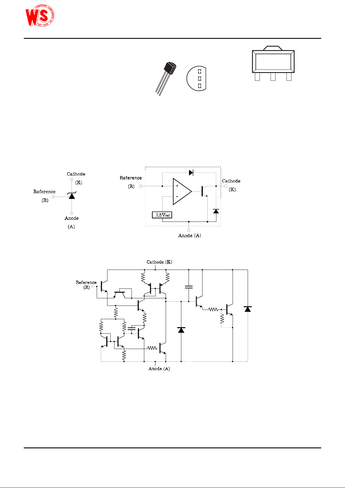
TO-92
REF
ANODE
CATHODE
SOT-89
REF
ANODE
CATHODE
TL431CLP
TL431CPK
FEATURES
• Programmable Output Voltage to 36V
• Low Dynamic Output Impedance 0.2Ω
• Sink Current Capability of 0.1 mA to 100 mA
• Equivalent Full-Range Temperature Coefficient of 50 ppm/
• Temperatu r e Compensated for Operation over Full Rated
Operating Temperatur e Range
• Low Output Noise Voltage
• Fast Turn on Response
DESCRIPTION
The TL431A is a three-terminal adjustable regulator series with a guaranteed thermal stability over applicable temperature ranges.
The output voltage may be set to any value between Vref (approximately 2.5 volts) and 36 volts with two external resistors. These
devices have a typical dynamic output impedance of 0.2Ω. Active output circuitry provides a very sharp turn-on characteristic,
making these devices excellent replacement for zener diodes in many applications.
The TL431A is characterized for operation from -0
o
C to +70oC.
SYMBOL FUNCTIONAL BLOCK DIAGRAM
o
C
SCHEMATIC DIAGRAM
Wing Shing Computer Components Co., (H.K.)Ltd. Tel:(852)2341 9276 Fax:(852)2797 8153
Homepage: http://www.wingshing.com E-mail: wsccltd@hkstar.com
1
TL431A Adjustable Precision Shunt Regulator
A
A
A
ABSOLUTE MAXIMUM RATINGS
(Operating temperature range applies unless otherwise specified)
Characteristic Symbol Value Unit
Cathode Voltage V
Cathode Current Range (Continuous) I
Reference Input Current Range I
Operating Temperatur e Range T
Storage Temperature Ran g e T
RECOMMENDED OPERATING CONDITIONS
Characteristic Symbol Test Condition Min Typ Max Unit
Cathode Voltage V
Cathode Current I
KA
K
ELECTRICAL CHARACTERISTICS
(TA = 25oC, unless otherwise specified)
Characteristic Symbol Test Condition Min Typ Max Unit
Reference Input Voltage V
Deviation of Reference Input Voltage
Over-Temperature (Note 1)
Ratio of Change in Reference Input
Voltage to the Change in
Cathode Voltage
Reference Input Current I
Deviation of Reference Input Current
Over Full Temperature Range
Minimum Cath od e Current for
Regulation
Off-State Cathode C urrent I
Dynamic Impedance (Note2) Z
V
REF(dev)
∆∆V
V
REF
I
REF(dev)
I
K(min)
K(off)
REF
KA
REF
KA
IK = 10mA
IK = 10mA, R1 = 10KΩ, R2 = ∞
IK = 10mA, R1 = 10KΩ, R2 = ∞
VKA = V
KA
K
REF
A
stg
VKA = V
VKA = V
, IK = 10mA 2.475 2.495 2.515 V
REF
, IK = 10mA
REF
≤ TA ≤ T
T
min
Ta = Full Range
VKA = V
VKA = 36V,
REF
VREF
, IK = 10mA to 100mA
f ≤ 1.0KHz
37 V
-100 ~ +150 mA
0.05 ~ +10 mA
0 ~ +70
-65 ~ +150
V
REF
36 V
1.0 100 mA
317 mV
max
∆V
∆K
KA =
KA =
10V-V
REF
36V- 10V
-1.4 -2.7
-1.0 -2.0
1,8 4
0.4 1.2
REF
0.5 1.0 mA
= 0 0.26 1.0
0.22 0.4
o
o
C
C
mV/V
µA
µA
µA
Ω
Note: 1. The deviation parameters V
REF(dev)
and I
are defined as the differences between the maximum and minimum values ob tained over t he rated
REF(dev)
temperature range.
V
REF(dev)
= V
(max) - V
REF
REF
(min)
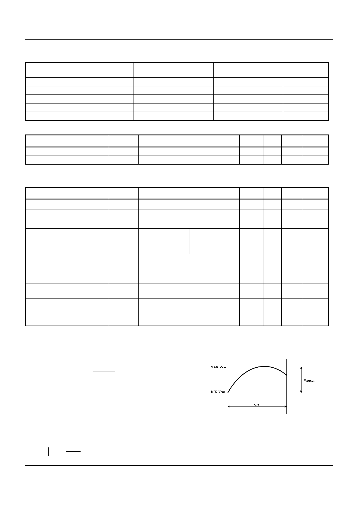
The equivalent full-range temperature coefficient of the reference
input voltage, αV
αV
( )
REF
ppm
C°
is defined as:
REF
( )
V@C
=
REF(dev)
V
REF
∆
°
Ta
× 10
6
Where ∆T
is the rated operating free-air temperature range of
A
the device.
αV
maximum V
can be positive or negative depending on whether minimum V
REF
respectively, occurs at the
REF
REF
or
lower temperature.
2. The dynamic impedance is defined as:
KA
∆
V
=
KA
Z
Wing Shing Computer Components Co., (H.K.)Ltd. Tel:(852)2341 9276 Fax:(852)2797 8153
Homepage: http://www.wingshing.com E-mail: wsccltd@hkstar.com
K
∆
I
2
 Loading...