

DDEESSCCRRIIPPTTIIOON
3-TERMINAL ADJUSTABLE REGULATORS
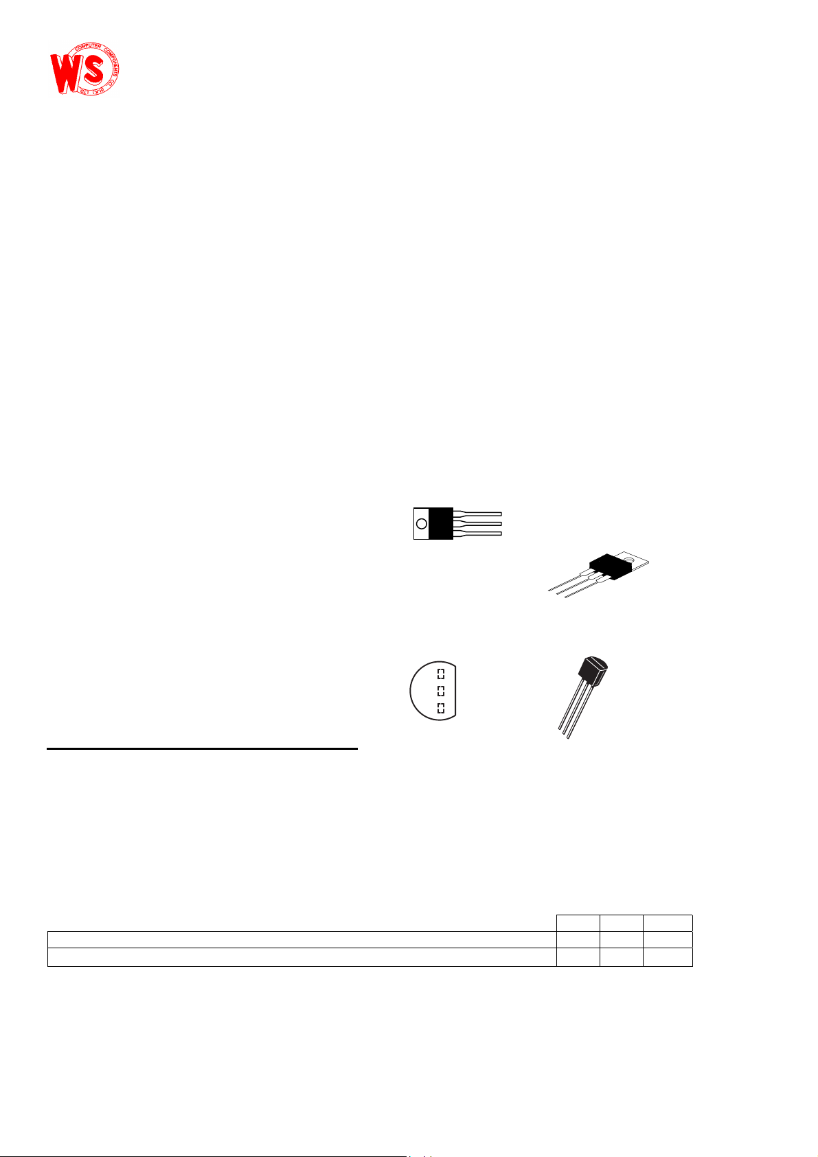
TO-220 PACKAGE
INPUT
OUTPUT
ADJUSTMENT
A
D
I
LM317
LM317T
AOI
TO-92
LM317LZ
INPUT
OUTPUT
ADJ
N
The LM317 are adjustable 3-terminal positive-voltage regulators capable of supplying 1.5A over
a differential voltage range of 3V to 40V. They are exceptionally easy to use and require only two
external resistors to set the output voltage. Both input and output regulation is better than
standard fixed regulators.
In addition to higher performance than fixed regulators, these regulators offer full overload
protection available only in integrated circuits. Included on the chip are current limit, thermal
overload protection, and safe-area protection. All overload protection circuit remains fully
functional even if the adjustment terminal is disconnected. Normally, no capacitors are needed
unless the device is situated far from the input filter capacitors in which case an input bypass is
needed. An optional output capacitor can be added to improve transient response.
The primary applications of each of these regulators is that of a programmable output regulator,
but by connecting a fixed resistor between adjustment terminal and the output terminal, each
device can be used as a precision current regulator. Even though the regulator is floating and
sees only the input-to-output differential voltage, use of these devices to regulate output voltages
that would cause the maximum-rated differential voltage to be exceeded if the output became
shorted is not recommended
FEATURES
!
Output Voltage Range Adjustable from 1.2 V to 37V
!
Output Current Capability of 1.5A Max
!
Input Regulation Typically 0.01% Per Input-Volt
Change
!
Output Regulation Typically 0.1%
!
Peak Output Current Constant over Temperature
Range of Regulator
!
Popular 3-Lead TO-220 AB Package
!
Ripple Rejection Typically 80 dB
ABSOLUTE MAXIMUM RATINGS
Input-Output Voltage Differential VI - V
Operating Junction Temperature Range
Continuous total dissipation at 25℃℃℃℃ free-air temperature
Continuous total dissipation at (or below ) 25℃℃℃℃ case temperature
Storage Temperature
Lead Temperature1.6 mm from case for 10 seconds
O
RECOMMENDED OPERATING CONDITIONS
OUTPUT CURRENT , I
OPERATING VIRTUAL JUNCTION TEMPERATURE,T
Wing Shing Computer Components Co., (H.K.)Ltd. Tel:(852)2341 9276 Fax:(852)2797 8153
Homepage: http://www.wingshing.com E-mail: wsccltd@hkstar.com
O
J
40V
0℃℃℃℃ to +125℃
2000mW
15W
–65℃℃℃℃ to +150℃
260℃
MIN MAX UNIT
10 1500 mA
07
0 ℃
℃
℃℃
℃
℃℃
℃
℃℃
ELECTRICAL CHARACTERISTICS
3-TERMINAL ADJUSTABLE REGULATORS
See Note 1
See Note 2
See Note 3
Uniess otherwise noted
,these specifications apply for the following test conditions:
Vi-Vo=5V and Io=0.5A. For conditions
shown as MIN or MAX, use the appropriate
value specified under recommended operating conditions.
*3
Output
voltage is calculated from
LM317
PARAMETER TEST CONDITIONS
Input Regulation*2 VI-VO=3V to 40V *3
MIN TYP MAX
TJ=MIN to MAX 0.01 0.04
I
=10mA to 1.5A 0.02 0.07
O
UNIT
%/V
VO=10V, f=120HZ 65
Ripple Rejection
Output Regulation
=10V, f=120HZ
V
O
10-µF capacitor between ADJ and ground
IO=10mA TO 1.5A,
=25℃*3,
T
J
=10mA to 1.5A
I
O
V
≤5V 5 25 mV
O
V
>5V 0.1 0.5 %
O
V
≥5V 20 70 mV
O
>5V 0.3 1.5 %
V
O
66 80
dB
Output Voltage Change With Temperature TJ=MIN to MAX 1 %
Output Voltage long-term Drift*4 After 1000h at TJ = MAX and VI-VO=40V 0.3 1 %
Output Noise Voltage
Minimum Output Current to Maintain
Regulation
Peak Output Current
f=10Hz to 10kHz, T
V
=40V 3.5 10 mA
I-VO
VI-V
≤15V
O
V
≤40V, T
I-VO
=25
J
=25℃
J
0.003 %
1.5 2.2
0.15 0.4
A
Adjustment-terminal Current 50 100 µA
=2.5V to 40V,
V
Change in adjustment-terminal Current
Reference Voltage(Output to ADJ)
I-VO
I
=10mA to 1.5A
O
V
VO=3V to 40V, IO=10mA to 1.5A,
-
I
P≤15W
1.20 1.25 1.30 V
0.2 5.0 µA
*1 All characteristics are measured with a 0.1-µF capacitor across the input and a 1-µF capacitor across the output.
*2 Input regulation is expressed here as the percentage change in output voltage per 1-V change at the input
*3 Pulse testing techniques are used to maintain the junction temperature as close to the ambient temperature a s possible.
Thermal effects must be taken into account separately.
*4 Since long-term drift cannot be measured on the individual devices prior to shipment. This specification is not intended to be a guarantee or warranty. It
is an engineering estimate of the average drift to be expected from lot to lot.
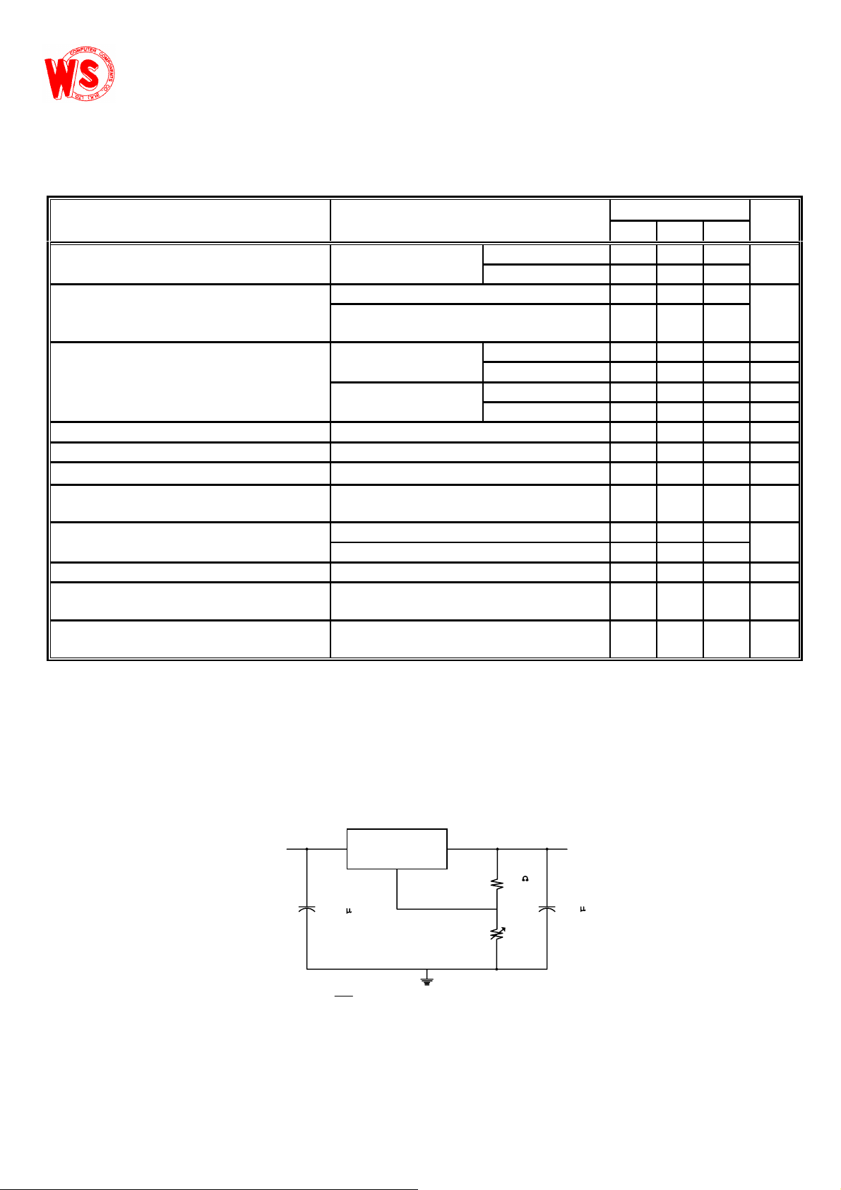
TYPICAL APPLICATION DATA
REG
ADJ
OUT
R
240
R
V
1
2
0
C2=1 F
V
I
VO = V
REF
IN
C1=0.1 F
R
2
{ 1+ }
R
1
1. Use of an input bypass capacitor is recommended if regulator is far from filter capacitors.
2. Use of an output capacitor improves transient response but is optional.
3. V
equals the difference between the output and adjustment terminal voltages.
REF

POSITIVE ADJUSTABLE REGULATOR
3-TERMINAL ADJUSTABLE REGULATORS
LM317
260
260
265
265
265265
260260
280
280
280280
3
240
240
240240
4
230
230
230230
Chip Size: 2.45X1.85mm
2
240
240
240240
1
240
240
240240
330
330
330330
PAD LOCATION LM317
PAD N PAD NAME
1 ADJ 2120 410
2 OUTPUT 1730 1490
3 INPUT 1120 950
4 OUTPUT 90 100
COORDINATES µm
XY
 Loading...