CURRENT−−MODE PWM CONTROLLER
Linear Integrated Circuit
have UVLO thresholds of 16 V(on) and 10 V (off).
operate
within 100%
duty cycle
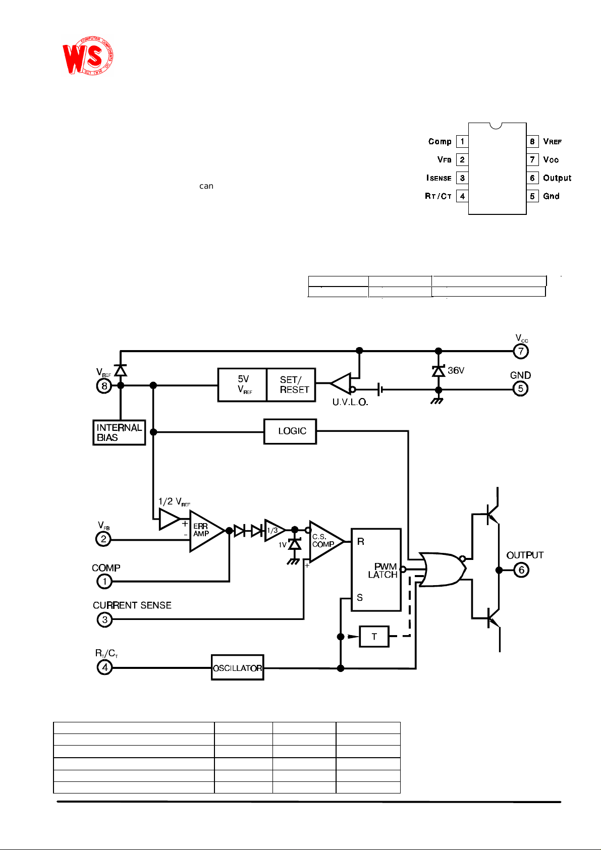
PIN CONNECTION
SO-8
1
in applications
using the same
external components as Motorola's parts,among others .The
DIP-8
SO-8
"
DIP-8
DIP-8
"
"
KA3842A
KA3842AM
KA3842AMM
KA3842AN
KA3842AMN
KA3842AM
KA3842A,KA3842AM
The KA3842A has been proven
KA3842AM
has been optimized for compatibility with Samsung's parts
Many applications can use either
KA3842A or KA3842AM
The KA3842A are fixe frequency current-mode
PWM controller. They are specially designed for OFF−Line and DC−to−DC converter
applications with minimal external components. These integrated circuits feature a
trimmed oscillator for precise duty cycle control, a temperature compensated reference,
high gain error amplifier, current sensing comparator, and a high current totempole
output ideally suited for driving a power MOSFET.
Protection circuity includes built under−voltage lockout and current limiting.
The
The KA3842A ,KA384AM can
The KA3842A have Start-Up Current 0,45 mA
FEATURES
ordering
• Low Start-Up Current
• Maximum Duty Cycle
• U/V Lockout With Hysteresis
• Operating Freguency Up To 500khz
BLOCK DIAGRAM
information
Device Package Operating temperature
KA3842AM SO-8 0 to +700C
Absolute Maximum Ratings
Characteristic Symbol Value Unit
Supply Voltage V
Output Current I
Analog Inputs V
Error Amp Output Sink Current I
Power Dissipation (TA=250C) P
Wing Shing Computer Components Co., (H.K.)Ltd. Tel:(852)2341 9276 Fax:(852)2797 8153
Homepage: http://www.wingshing.com E-mail: wsccltd@hkstar.com
CC
O
I
SINK (E.A)
O
30 V
±1
−0.3 to V
CC
10 mA
1 W
A
V

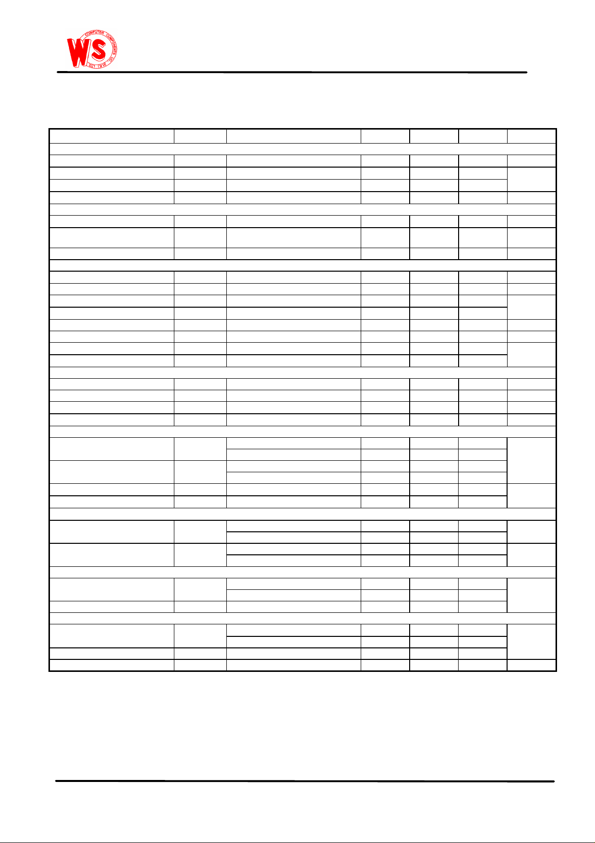
Electrical characteristics (*VCC=15V, RT=10kΩΩ, CT=3.3nF, TA=00C to +700C, unless
2
KA3842A/KA3842AM
otherwise specified)
Characteristics Symbol Test Condition Min Typ Max Unit
Reference Section
Reference Output Voltege V
Line Regulation
Load Regulation
Short Circit Output Current I
∆V
∆V
REF
REF
REF
SC
Oscillator Section
Oscillation Freguency f
Frequency Change with
∆f/∆V
Voltage
Oscillator Amplitude V
(OSC)
Error Amplifier Section
Input Bias Current I
Input Voltage V
Open Loop Voltage Gain G
BIAS
I(E.A)
VO
Power Supply Rejection Ratio PSRR
Output Sink Current I
Output Source Current I
High Output Voltage V
Low Output Voltage V
SINK
SOURCE
OH
OL
Current Sense Section
Gain G
Maximum Input Signal V
V
I(MAX)
Power Supply Rejection Ratio PSRR
Input Bias Current I
BIAS
Output Section
Low Output Voltage V
High Output Voltage V
Rise Time t
Fall Time t
OL
OH
R
F
Under−−Voltage Lockout Section
Start Theshold V
TH(ST)
TJ = 25°C, I
= 1 mA
REF
12V ≤ VCC ≤ 25 V
1 mA ≤ I
≤ 20mA
REF
TA = 25°C
T
= 25°C
J
12V ≤ VCC ≤ 25 V
CCF
V1 = 2.5V 2.42 2.5 2.58 V
2V ≤ V0 ≤ 4V
12V ≤ V
≤ 25 V
CC
V2 = 2.7V, V1 = 1.1V 2 7 mA
V2 = 2.3V, V1 = 5V -0.5 -1.0 mA
V2 = 2.3V, RL = 15KΩ to GND
V2 = 2.7V, RL = 15KΩ to PIN 8
(Note 1 & 2) 2.85 3.0 3.15 V/V
V1 = 5V (Note1) 0.9 1.0 1.1 V
12V ≤ V
I
SINK
I
SINK
I
SINK
I
SINK
≤ 25 V (Note 1)
CC
= 20 mA 0.08 0.4
= 200 mA 1.4 2.2 V
= 20 mA 13 13.5
= 200 mA 12 13.0
TJ = 25°C, CL = 1nF (Note 3)
TJ = 25°C, CL = 1nF (Note 3)
14.5 16.0 17.5 V
4.9 5.0 5.1 V
6.0 20 mV
6.0 25
-100 -180 mA
47 52 57 KHz
0.05 1.0 %
1.6 V
-0.1 -2
65 90 dB
60 70
5.0 6.0 V
0.8 1.1
70 dB
-3.0 -10
45 150 nS
35 150
p-p
µA
µA
Min. Operating Voltage V
(After Turn On)
PWM Section
Max. Duty Cycle D
Min. Duty Cycle D
Total Standby Current
Start−Up Current
Operating Supply Current I
Zener Voltage V
* Adjust VCC above the start threshold before setting at 15V
Note 1: Parameter measured at trip point of lath with V
Note 2: Gain defined as A=∆V
Note 3: These parameters, although guaranteed, are not 100% tested in production.
OPR(min)
(MAX)
(MAX)
I
ST
CC (OPR)V3
/∆V3 ; 0 ≤ V3 ≤ 0.8V
1
8.5 10 11.5 V
95 97 100
0.17 0.3 mA
= V2 = 0V 14 17
Z
%
0
30 38 V
=0
2
 Loading...