

Winbond Electronics W986432AH Datasheet
W986432AH
512K × 4 BANKS × 32 BITS SDRAM
GENERAL DESCRIPTION
W986432AH is a high-speed synchronous dynamic random access memory (SDRAM), organized as
512K words × 4 banks × 32 bits. Using pipelined architecture and 0.20 µm process technology,
W986432AH delivers a data bandwidth of up to 732M bytes per second (-55). For different
application, W986432AH is sorted into four speed grades: -55, -6, -7 and -8.
Accesses to the SDRAM are burst oriented. Consecutive memory location in one page can be
accessed at a burst length of 1, 2, 4, 8 or full page when a bank and row is selected by an ACTIVE
command. Column addresses are automatically generated by the SDRAM internal counter in burst
operation. Random column read is also possible by providing its address at each clock cycle. The
multiple bank nature enables interleaving among internal banks to hide the precharging time.
By having a programmable Mode Register, the system can change burst length, latency cycle,
interleave or sequential burst to maximize its performance. W986432AH is ideal for main memory in
high performance applications.
FEATURES
•
3.3V ±0.3V power supply
•
524288 words × 4 banks × 32 bits organization
•
Auto Refresh and Self Refresh
•
CAS latency: 2 and 3
•
Burst Length: 1, 2, 4, 8, and full page
•
Sequential and Interleave burst
•
Burst read, single write operation
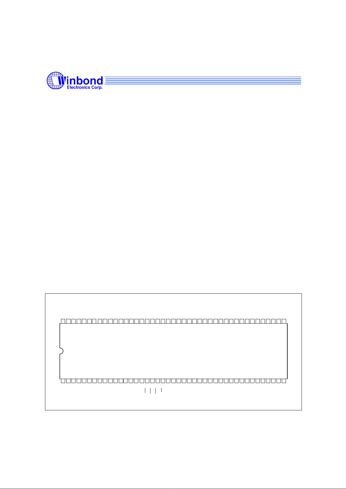
PIN CONFIGURATION
Q
Q
SS
VssDQ15
86
85
2345678
1
DQ0
VCC
CC
V
DQ14
DQ13
V
DQ12
DQ11
84838281807978777675747372717069686766656463626160
Q
Q
SS
CC
DQ1
DQ2
DQ3
DQ4
V
V
Q
Q
SS
CC
V
DQ10
DQ9
V
DQ8NCVSSDQM1NCNC
9
1011121314151617181920212223242526
Q
CC
DQ5
V
DQ6
VSSQ
DQ7
NC
VCC
DQM0
CLK
WE
CAS
RAS
•
Byte data controlled by DQM
•
Power-down Mode
•
Auto-precharge and controlled precharge
•
4K refresh cycles/64 mS
•
Interface: LVTTL
•
Packaged in 86-pin TSOP II, 400 mil - 0.50
CKEA9A8A7A6A5A4A3DQM3
59
27
282930313233343536
BS0
BS1
A10/AP
A0A1A2
DQM2
CS
NC
Q
CC
VSSNC
DQ31
V
DQ30
DQ29
58575655545352
Q
CC
NC
V
SS
V
DQ16
DQ17
DQ18
Q
Q
SS
CC
V
DQ28
DQ27
V
50494847464544
51
37383940414243
Q
Q
SS
CC
V
DQ19
DQ20
V
DQ26
DQ21
DQ25
DQ22
Q
SS
SS
V
DQ24
V
Q
CC
V
CC
V
DQ23
Publication Release Date: December 1999
- 1 - Revision A1
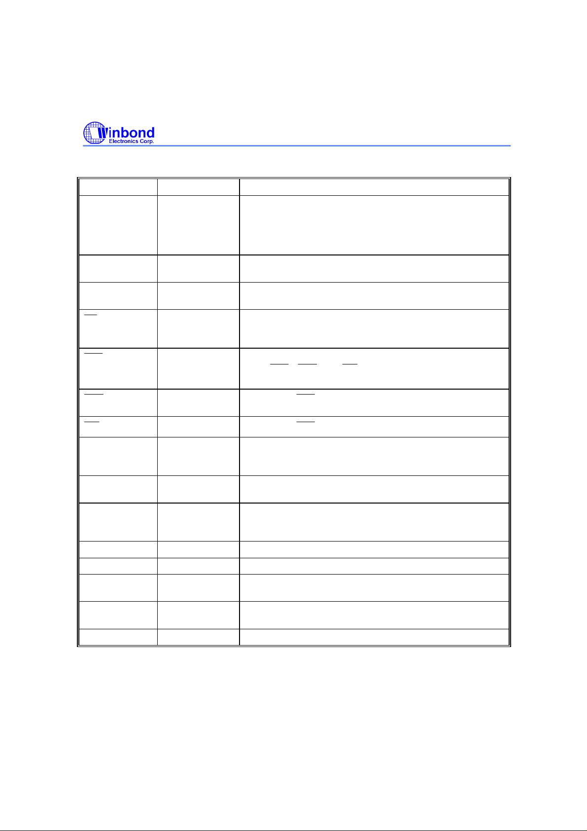
PIN DESCRIPTION
Select bank to activate during row address latch time, or bank
CS
RAS
RAS, CAS
CAS
RAS WE
RAS
Input/output mask
Power (+3.3V) for
PIN NAME FUNCTION DESCRIPTION
W986432AH
A0−A10
BS0, BS1 Bank Select
DQ0−DQ31
DQM0−
DQM3
CLK Clock Inputs System clock used to sample inputs on the rising edge of
CKE Clock Enable CKE controls the clock activation and deactivation. When
VCC Power (+3.3V) Power for input buffers and logic circuit inside DRAM.
VSS Ground Ground for input buffers and logic circuit inside DRAM.
CCQ
V
SSQ
V
Ground for I/O
NC No Connection No connection
Address Multiplexed pins for row and column address.
Row address: A0−A10. Column address: A0−A7.
A10 is sampled during a precharge command to determine if
all banks are to be precharged or bank selected by BS0, BS1.
to read/write during address latch time.
Data Input/
Output
Chip Select Disable or enable the command decoder. When command
Row Address
Strobe
Column Address
Strobe
Write Enable
I/O buffer
buffer
Multiplexed pins for data output and input.
decoder is disabled, new command is ignored and previous
operation continues.
Command input. When sampled at the rising edge of the
clock
executed.
Referred to
Referred to
The output buffer is placed at Hi-Z (with latency of 2) when
DQM is sampled high in read cycle. In write cycle, sampling
DQM high will block the write operation with zero latency.
clock.
CKE is low, Power Down mode, Suspend mode, or Self
Refresh mode is entered.
Separated power from VCC, to improve DQ noise immunity.
Separated ground from VSS, to improve DQ noise immunity.
and WE define the operation to be
- 2 -
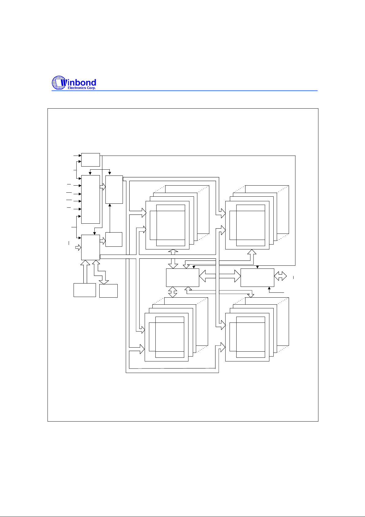
BLOCK DIAGRAM
W986432AH
CLK
CKE
RAS
CAS
A10
BS0
BS1
CLOCK
BUFFER
GENERATOR
MODE
REGISTER
COLUMN
COUNTER
CONTROL
SIGNAL
COLUMN DECODER
CELL ARRAY
BANK #0
ROW DECODER
SENSE AMPLIFIER
COLUMN DECODER
DATA CONTROL
CIRCUIT
COLUMN DECODER
CELL ARRAY
BANK #1
ROW DECODERROW DECODER
SENSE AMPLIFIER
COLUMN DECODER
DQ
BUFFER
DQ0
DQ31
DQM0~3
CS
COMMAND
DECODER
WE
A0
ADDRESS
A9
BUFFER
REFRESH
COUNTER
CELL ARRAY
BANK #2
ROW DECODER
SENSE AMPLIFIER
CELL ARRAY
BANK #3
SENSE AMPLIFIER
NOTE:
The cell array configuration is 2048 * 256 * 32
Publication Release Date: December 1999
- 3 - Revision A1

W986432AH
RAS, CAS, CS
RAS
CAS
FUNCTIONAL DESCRIPTION
Power Up and Initialization
The default power up state of the mode register is unspecified. The following power up and
initialization sequence need to be followed to guarantee the device being preconditioned to each user
specific needs.
During power up, all VCC and V
when the input signals are held in the "NOP" state. The power up voltage must not exceed V
on any of the input pins or VCC supplies. After power up, an initial pause of 200 µS is required
followed by a precharge of all banks using the precharge command. To prevent data contention on
the DQ bus during power up, it is required that the DQM and CKE pins be held high during the initial
pause period. Once all banks have been precharged, the Mode Register Set Command must be
issued to initialize the Mode Register. An additional eight Auto Refresh cycles (CBR) are also
required before or after programming the Mode Register to ensure proper subsequent operation.
Programming Mode Register
After initial power up, the Mode Register Set Command must be issued for proper device operation.
All banks must be in a precharged state and CKE must be high at least one cycle before the Mode
Register Set Command can be issued. The Mode Register Set Command is activated by the low
signals of
this cycle defines the parameters to be set as shown in the Mode Register Operation table. A new
command may be issued following the mode register set command once a delay equal to t
elapsed. Please refer to the next page for Mode Register Set Cycle and Operation Table.
CCQ
pins must be ramp up simultaneously to the specified voltage
CC
+0.3V
and WE at the positive edge of the clock. The address input data during
RSC
has
Bank Activate Command
The Bank Activate command must be applied before any Read or Write operation can be executed.
The operation is similar to RAS activate in EDO DRAM. The delay from when the Bank Activate
command is applied to when the first read or write operation can begin must not be less than the RAS
to CAS delay time (t
Activate command can be issued to the same bank. The minimum time interval between successive
Bank Activate commands to the same bank is determined by the RAS cycle time of the device (tRC).
The minimum time interval between interleaved Bank Activate commands (Bank A to Bank B and
vice versa) is the Bank to Bank delay time (t
active is specified as T
RCD
). Once a bank has been activated it must be precharged before another Bank
RRD
). The maximum time that each bank can be held
RAS
(max.).
Read and Write Access Modes
After a bank has been activated, a read or write cycle can be followed. This is accomplished by
setting
level defines whether the access cycle is a read operation (WE high), or a write operation (WE low).
The address inputs determine the starting column address. Reading or writing to a different row within
an activated bank requires the bank be precharged and a new Bank Activate command be issued.
When more than one bank is activated, interleaved bank Read or Write operations are possible. By
using the programmed burst length and alternating the access and precharge operations between
multiple banks, seamless data access operation among many different pages can be realized. Read
or Write Commands can also be issued to the same bank or between active banks on every clock
cycle.
high and
low at the clock rising edge after minimum of tRCD delay. WE pin voltage
- 4 -

Burst Read Command
CAS
RAS
CAS
RAS
RAS
CAS
W986432AH
The Burst Read command is initiated by applying logic low level to CS and
and WE high at the rising edge of the clock. The address inputs determine the starting column
address for the burst. The Mode Register sets type of burst (sequential or interleave) and the burst
length (1, 2, 4, 8, full page) during the Mode Register Set Up cycle. Table 2 and 3 in the next page
explain the address sequence of interleave mode and sequence mode.
while holding
Burst Command
The Burst Write command is initiated by applying logic low level to CS,
high at the rising edge of the clock. The address inputs determine the starting column address.
Data for the first burst write cycle must be applied on the DQ pins on the same clock cycle that the
Write Command is issued. The remaining data inputs must be supplied on each subsequent rising
clock edge until the burst length is completed. Data supplied to the DQ pins after burst finishes will be
ignored.
and WE while holding
Read Interrupted by a Read
A Burst Read may be interrupted by another Read Command. When the previous burst is interrupted,
the remaining addresses are overridden by the new read address with the full burst length. The data
from the first Read Command continues to appear on the outputs until the CAS latency from the
interrupting Read Command the is satisfied.
Read Interrupted by a Write
To interrupt a burst read with a Write Command, DQM may be needed to place the DQs (output
drivers) in a high impedance state to avoid data contention on the DQ bus. If a Read Command will
issue data on the first and second clocks cycles of the write operation, DQM is needed to insure the
DQs are tri-stated. After that point the Write Command will have control of the DQ bus and DQM
masking is no longer needed.
Write Interrupted by a Write
A burst write may be interrupted before completion of the burst by another Write Command. When
the previous burst is interrupted, the remaining addresses are overridden by the new address and
data will be written into the device until the programmed burst length is satisfied.
Write Interrupted by a Read
A Read Command will interrupt a burst write operation on the same clock cycle that the Read
Command is activated. The DQs must be in the high impedance state at least one cycle before the
new read data appears on the outputs to avoid data contention. When the Read Command is
activated, any residual data from the burst write cycle will be ignored.
Burst Stop Command
A Burst Stop Command may be used to terminate the existing burst operation but leave the bank
open for future Read or Write Commands to the same page of the active bank, if the burst length is
full page. Use of the Burst Stop Command during other burst length operations is illegal. The Burst
Stop Command is defined by having
the clock. The data DQs go to a high impedance state after a delay, which is equal to the CAS
Publication Release Date: December 1999
- 5 - Revision A1
and
high with CS and WE low at the rising edge of
W986432AH
Latency in a burst read cycle, interrupted by Burst Stop. If a Burst Stop Command is issued during a
full page burst write operation, then any residual data from the burst write cycle will be ignored.
Addressing Sequence of Sequential Mode
A column access is performed by increasing the address from the column address which is input to
the device. The disturb address is varied by the Burst Length as shown in Table 2
Table 2 Address Sequence of Sequential Mode
.
DATA ACCESS ADDRESS
Data 0 n BL = 2 (disturb address is A0)
Data 1 n + 1 No address carry from A0 to A1
Data 2 n + 2 BL = 4 (disturb addresses are A0 and A1)
Data 3 n + 3 No address carry from A1 to A2
Data 4 n + 4
Data 5 n + 5 BL = 8 (disturb addresses are A0, A1 and A2)
Data 6 n + 6 No address carry from A2 to A3
Data 7 n + 7
BURST LENGTH
Addressing Sequence of Interleave Mode
A column access is started in the input column address and is performed by inverting the address bit
in the sequence shown in Table 3.
Table 3 Address Sequence of Interleave Mode
DATA ACCESS ADDRESS BUST LENGTH
Data 0 A8 A7 A6 A5 A4 A3 A2 A1 A0 BL = 2
Data 1
Data 2
Data 3
Data 4
Data 5
Data 6
Data 7
A8 A7 A6 A5 A4 A3 A2 A1 A0
A8 A7 A6 A5 A4 A3 A2 A1 A0
A8 A7 A6 A5 A4 A3 A2 A1 A0
A8 A7 A6 A5 A4 A3 A2 A1 A0
A8 A7 A6 A5 A4 A3 A2 A1 A0
A8 A7 A6 A5 A4 A3 A2 A1 A0
A8 A7 A6 A5 A4 A3 A2 A1 A0
BL = 4
BL = 8
- 6 -

W986432AH
RAS
CAS
RAS, CAS
Auto-precharge Command
If A10 is set to high when the Read or Write Command is issued, then the auto-precharge function is
entered. During auto-precharge, a Read Command will execute as normal with the exception that the
active bank will begin to precharge automatically before all burst read cycles have been completed.
Regardless of burst length, it will begin a certain number of clocks prior to the end of the scheduled
burst cycle. The number of clocks is determined by CAS latency.
A Read or Write Command with auto-precharge cannot be interrupted before the entire burst
operation is completed for the same bank. Therefore, use of a Read, Write, or Precharge Command
is prohibited during a read or write cycle with auto-precharge. Once the precharge operation has
started, the bank cannot be reactivated until the Precharge time (tRP) has been satisfied. Issue of
Auto-Precharge command is illegal if the burst is set to full page length. If A10 is high when a Write
Command is issued, the Write with Auto-Precharge function is initiated. The SDRAM automatically
enters the precharge operation one clock delay from the last burst write cycle. This delay is referred
to as write t
satisfied. This is referred to as t
DPL
. The bank undergoing auto-precharge cannot be reactivated until t
DAL
, Data-in to Active delay (t
DAL
DPL
= t
+ tRP). When using the Autoprecharge Command, the interval between the Bank Activate Command and the beginning of the
internal precharge operation must satisfy t
RAS
(min).
Precharge Command
The Precharge Command is used to precharge or close a bank that has been activated. The
Precharge Command is entered when CS,
of the clock. The Precharge Command can be used to precharge each bank separately or all banks
simultaneously. Three address bits, A10, BS0, and BS1 are used to define which bank(s) is to be
precharged when the command is issued. After the Precharge Command is issued, the precharged
bank must be reactivated before a new read or write access can be executed. The delay between the
Precharge Command and the Activate Command must be greater than or equal to the Precharge
time (tRP).
and WE are low and
is high at the rising edge
DPL
and tRP are
Self Refresh Command
The Self Refresh Command is defined by having CS,
at the rising edge of the clock. All banks must be idle prior to issuing the Self Refresh Command.
Once the command is registered, CKE must be held low to keep the device in Self Refresh mode.
When the SDRAM has entered Self Refresh mode all of the external control signals, except CKE, are
disabled. The clock is internally disabled during Self Refresh Operation to save power. The device
will exit Self Refresh operation after CKE is returned high. A minimum delay time is required when
the device exits Self Refresh Operation and before the next command can be issued. This delay is
equal to the tAC cycle time plus the Self Refresh exit time.
If, during normal operation, AUTO REFRESH cycles are issued in bursts (as opposed to being evenly
distributed), a burst of 4,096 AUTO REFRESH cycles should be completed just prior to entering and
just after exiting the self refresh mode.
and CKE held low with WE high
Power Down Mode
The Power Down mode is initiated by holding CKE low. All of the receiver circuits except CKE are
gated off to reduce the power. The Power Down mode does not perform any refresh operations,
therefore the device can not remain in Power Down mode longer than the Refresh period (t
device.
Publication Release Date: December 1999
- 7 - Revision A1
REF
) of the

W986432AH
RAS, CAS
RAS, CAS
The Power Down mode is exited by bringing CKE high. When CKE goes high, a No Operation
Command is required on the next rising clock edge, depending on tCK. The input buffers need to be
enabled with CKE held high for a period equal to t
CES
(min.) + t
No Operation Command
The No Operation Command should be used in cases when the SDRAM is in a idle or a wait state to
prevent the SDRAM from registering any unwanted commands between operations. A No Operation
Command is registered when CS is low with
clock. A No Operation Command will not terminate a previous operation that is still executing, such
as a burst read or write cycle.
Deselect Command
The Deselect Command performs the same function as a No Operation Command. Deselect
Command occurs when CS is brought high, the
Clock Suspend Mode
During normal access mode, CKE must be held high enabling the clock. When CKE is registered low
while at least one of the banks is active, Clock Suspend Mode is entered. The Clock Suspend mode
deactivates the internal clock and suspends any clocked operation that was currently being executed.
There is a one clock delay between the registration of CKE low and the time at which the SDRAM
operation suspends. While in Clock Suspend mode, the SDRAM ignores any new commands that are
issued. The Clock Suspend mode is exited by bringing CKE high. There is a one clock cycle delay
from when CKE returns high to when Clock Suspend mode is exited.
CK
(min.).
, and WE held high at the rising edge of the
, and WE signals become don't cares.
- 8 -
W986432AH
TABLE OF OPERATING MODES
Fully synchronous operations are performed to latch the commands at the positive edges of CLK.
Table 1 shows the truth table for the operation commands.
TABLE 1 TRUTH TABLE (NOTE (1), (2))
Command
Bank Active Idle H x x v v V L L H H
Bank Precharge Any H x x v L x L L H L
Precharge All Any H x x x H x L L H L
Write Active (3) H x x v L v L H L L
Write with Autoprecharge Active (3) H x x v H v L H L L
Read Active (3) H x x v L v L H L H
Read with Autoprecharge Active (3) H x x v H v L H L H
Mode Register Set Idle H x x v v v L L L L
No-Operation Any H x x x x x L H H H
Burst Stop Active (4) H x x x x x L H H L
Device Deselect Any H x x x x x H x x x
Auto-Refresh Idle H H x x x x L L L H
Self-Refresh Entry Idle H L x x x x L L L H
Self Refresh Exit idle
Clock suspend Mode
Entry
Power Down Mode Entry Idle
Clock Suspend Mode Exit Active L H x x x x x x x X
Power Down Mode Exit Any
Data write/Output Enable Active H x L x x x x x x x
Data Write/Output Disable Active H x H x x x x x x x
Notes:
(1) v = valid, x = Don't care, L = Low Level, H = High Level
(2) CKEn signal is input leve l when commands are provided.
(3) These are state of bank designated by BS0, BS1 signals.
(4) Device state is full page burst operation.
(5) Power Down Mode can not be entered in the burst cycle.
When this command asserts in the burst cycle, device state is clock suspend mode.
Device state CKEn-1 CKEn
L
(S.R)
Active H L x x x x x x x x
Active (5)
(power
down)
L
H
H
L
L
DQM BS0, 1 A10 A0-A9
H
H
L
L
H
H
x
x
x
x
x
x
x
x
x
x
x
x
RAS CAS
CS
x
x
x
x
x
x
x
H L x
x
x
x
x
x
H x H x x
H L x
H x H X H
H L x
H x H X H
WE
Publication Release Date: December 1999
- 9 - Revision A1
W986432AH
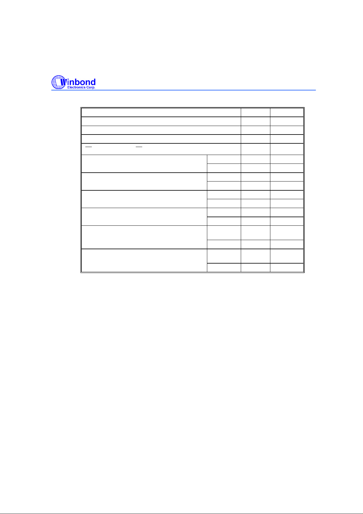
DC CHARACTERISTICS
Absolute Maximum Rating
PARAMETER SYM. RATING UNIT NOTES
Input, Column Output Voltage
Power Supply Voltage
Operating Temperature
Storage Temperature
Soldering Temperature (10s)
Power Dissipation
Short Circuit Output Current
Note: Exposure to conditions beyond those listed under Absolute Maximum Ratings may adversely affect the life and reliability of the
device.
OUT
VIN, V
CC, VCCQ -0.3 − 4.6
V
T
T
SOLDER
T
I
OPR
STG
D
P
OUT
-0.3 − V
CC
+0.3
0 − 70
-55 − 150
260 °C 1
1 W 1
50 mA 1
RECOMMENDED DC OPERATING CONDITIONS
(TA = 0 to 70°C)
V 1
V 1
°
C 1
°C 1
PARAMETER SYM. MIN. TYP. MAX. UNIT NOTE
CCQ
V
CC
Power Supply Voltage V
Power Supply Voltage (for I/O
Buffer)
Input High Voltage V
Input Low Voltage V
Note: VIH (max.) = VCC/VCCQ+1.2V for pulse width < 5 nS
IL
V
(min.) = VSS/VSSQ-1.2V for pulse width < 5 nS
IH
IL
CAPACITANCE
(VDD = 3.3V, TA = 25 °C, f = 1 MHz)
PARAMETER SYM. MIN. MAX. UNIT
Input Capacitance
(A0 to A11, BS0, BS1, CS,
Input Capacitance (CLK)
Input/Output capacitance (DQ0−DQ31)
Note: These parameters are periodically sampled and not 100% tested
RAS, CAS
, WE, DQM, CKE)
S
3.0 3.3 3.6 V 2
3.0 3.3 3.6 V 2
2.0 - VCC +0.3 V 2
-0.3 - 0.8 V 2
I
C
O
C
2.5 4 pf
2.5 4 pf
4 6.5 pf
- 10 -
DC CHARACTERISTICS
(VCC = 3.3V ±0.3V, TA = 0°~70°C)
PARAMETER SYM. -55 -6 -7 -8 UNIT NOTES
Operating Current
tCK = min., tRC = min.
Active precharge command
cycling without burst operation
Standby Current
tCK = min., CS= VIH
VIH/L = VIH (min.)/VIL (max.)
Bank: inactive state CKE = VIL (Power
Standby Current
CLK = VIL, CS= VIH
VIH/L=VIH (min.)/VIL (max.)
BANK: inactive state CKE = VIL (Power
No Operating Current
tCK = min., CS= VIH (min.)
BANK: active state (4 banks) CKE = VIL (Power
Burst Operating Current (tCK = min.)
Read/Write command cycling
Auto Refresh Current (tCK = min.)
Auto refresh command cycling
Self Refresh Current (CKE = 0.2V)
Self refresh mode
1 bank operation
CKE = VIH
Down mode)
CKE = VIH
Down mode)
CKE = VIH
Down mode)
W986432AH
MAX. MAX. MAX. MAX.
CC1
I
ICC2 55 50 45 40 3
CC2P
I
ICC2S 8 8 8 8
ICC2PS 1 1 1 1 mA
ICC3 70 65 55 45
ICC3P 3 3 3 3
CC4
I
ICC5 145 135 125 105 3
ICC6 1 1 1 1
105 100 90 80 3
1 1 1 1 3
160 155 145 125 3, 4
PARAMETER SYMBOL MIN. MAX. UNIT NOTES
Input Leakage Current
(0V
VIN
VCC, all other pins not under test = 0V)
≤
≤
Output Leakage Current
7(Output disable, 0V ≤ VOUT ≤ VCCQ)
LVTTL Output ″H″ Level Voltage
(IOUT = -2 mA)
LVTTL Output
OUT
(I
= 2 mA)
"
L″ Level Voltage
II(L) -5 5
VO(L) -5 5
VOH 2.4 - V
VOL - 0.4 V
A
µ
A
µ
Publication Release Date: December 1999
- 11 - Revision A1
W986432AH
AC CHARACTERISTICS
(V
= 3.3V ± 0.3V, V
CC
PARAMETER
Ref/Active to Ref/Active Command Period t
Active to precharge Command Period tRAS 38.5 100000 42 100000 48 100000 48 100000 9
Active to Read/Write Command Delay Time tRCD 16.5
Read/Write(a) to Read/Write(b)Command
Period
Precharge to Active(b) Command Period tRP 18 18 20 20 nS 9
Active(a) to Active(b) Command Period tRPD 11 12 14 16 9
Write Recovery Time
CLK Cycle Time
CLK High Level
CLK Low Level
Access Time from CLK
Output Data Hold Time tOH 2 2 2.5 3
Output Data High Impedance Time tHZ 2 5.5 2 6 2.5 7 3 8 8
Output Data Low Impedance Time tLZ 0 0 0 0
Power Down Mode Entry Time t
Transition Time of CLK (Rise and Fall) tT 0.3 10 0.3 10 0.3 10 0.3 10
Data-in-Set-up Time tDS 1.5 2 2 2
Data-in Hold Time t
Address Set-up Time tAS 1.5 2 2 2
Address Hold Time tAH 1 1 1 1
CKE Set-up Time t
CKE Hold Time tCKH 1 1 1 1
Command Set-up Time tCMS 1.5 2 2 2
Command Hold Time t
Refresh Time tREF 64 64 64 64 mS
Mode Register Set Cycle Time tRSC 11 12 14 16 nS 9
= 0V, Ta = 0 to 70 °C) (Notes: 5, 6, 7, 11)
SS
-55 -6 -7 -8 UNIT NOTE
CL* = 2
CL* = 3
CL* = 2
CL* = 3
CL* = 2
CL* = 3
MIN. MAX. MIN. MAX. MIN. MAX. MIN. MAX.
RC
60 60 70 72 nS 9
CCD
t
1 1 1 1 Cycle 9
WR
t
10 10 10 10
5.5 6 7 8
tCK 10 1000 10 1000 10 1000 10 1000
5.5 1000 6 1000 7 1000 8 1000
tCH 2 2.5 3 3 10
tCL 2 2.5 3 3 10
tAC 7 7 7 7
5 5.5 5.5 6
SB
0 5.5 0 6 0 7 0 8
DH
1 1 1 1
CKS
1.5 2 2 2
CMH
1 1 1 1
18 20 20 9
- 12 -
W986432AH
(2) A.C Latency Characteristics
CKE to clock disable (CKE Latency) 1 Cycle
DQM to output to HI-Z (Read DQM Latency) 2
DQM to output to HI-Z (Write DQM Latency) 0
Write command to input data (Write Data Latency) 0
to Command input (CS Latency)
CS
Precharge to DQ Hi-Z Lead time CL = 2 2
CL = 3 3
Precharge to Last Valid data out CL = 2 1
CL = 3 2
Bust Stop Command to DQ Hi-Z Lead time CL = 2 2
CL = 3 3
Bust Stop Command to Last Valid Data out CL = 2 1
CL = 3 2
Read with Auto-precharge Command to Active/Ref
Command
CL = 3 BL + tRP
Write with Auto-precharge Command to Active/Ref
Command
CL = 3 BL + tRP
CL = 2 BL + tRP Cycle + nS
CL = 2 BL + tRP
0
- 14 -

W986432AH
Notes:
1. Operation exceeds "ABSOLUTE MAXIMUM RATING" may cause permanent damage to the
devices.
2. All voltages are referenced to VSS
3. These parameters depend on the cycle rate and listed values are measured at a cycle rate with the
minimum values of tCK and tRC.
4. These parameters depend on the output loading conditions. Specified values are obtained with
output open.
5. Power up Sequence
(1) Power up must be performed in the following sequence.
(2) Power must be applied to VCC and VCCQ (simultaneously) while all input signals are held in the “NOP” state. The CLK
signals must be started at the same time.
(3) After power-up a pause of at least 200 ìseconds is required. It is required that DQM and CKE signals then be held ‘
high‘ (VCC levels) to ensure that the DQ output is impedance.
(4) All banks must be precharged.
(5) The Mode Register Set command must be asserted to initialize the Mode Register.
(6) A minimum of eight Auto Refresh dummy cycles is required to stabilize the internal circuitry of the device.
6. AC Testing Conditions
PARAMETER CONDITIONS
Output Reference Level 1.4V
Output Load See diagram below
Input Signal Levels (VIH/VIL) 2.4V/0.4V
Transition Time (Rise and Fall) of Input Signal 1 nS
Input Reference Level 1.4V
1.4 V
50 ohms
Z = 50 ohmsoutput
AC TEST LOAD
1. Transition times are measured between VIH and VIL.
2. tHZ defines the time at which the outputs achieve the open circuit condition and is not referenced to output level.
3. These parameters account for the number of clock cycles and depend on the operating frequency of the clock, as
follows the number of clock cycles = specified value of timing/ clock period
(count fractions as whole number)
(1) tCH is the pulse width of CLK measured from the positive edge to the negative edge referenced to VIH (min.).
tCL is the pulse width of CLK measured from the negative edge to the positive edge referenced to VIL (max.).
30pF
Publication Release Date: December 1999
- 13 - Revision A1
 Loading...