

Winbond Electronics W91F813AN, W91F812N, W91F812AN, W91F811AN, W91F811ALN Datasheet
...
W91F810N SERIES
23-FLASH MEMORY TONE/PULSE DIALER WITH
HANDFREE, LOCK AND HOLD FUNCTIONS
GENERAL DESCRIPTION
The W91F810N is a series of tone/pulse switchable telephone dialers with 23-falsh memory, keytone,
hold, lock, mute, volume control and handfree dialing control features. These chips are fabricated
using Winbond's high-performance CMOS technology and thus offer good performance in lowvoltage, low-power operations.
FEATURES
• Tone/pulse switchable dialer
• Two by 32 digits redial and save memory
• Three by 32 digits one-touch direct repertory flash-memory
• Twenty by 32 digits one-touch direct or two-touch indirect repertory flash-memory
• The read-write times: 10
• Pulse-to-tone (*/T) keypad for long distance call operation
• Chain dialing
• Uses 6
×
6 or 7 × 7 keyboard
• Easy operation with redial, flash, pause, and */T keypads
• Pause, P
→
T (pulse-to-tone) can be stored as a digit in memory
• Dialing rate: 10 or 20 ppS by mask option
• Minimum tone output duration: 93 mS
• Minimum intertone pause: 93 mS
• Pause time: 3.6 sec.
• Flash break time (73 mS, 100 mS, 300 mS, or 600 mS) selectable by keypad; pause time is 1.0 S
• Make/break ratio (2:3 or 1:2) selectable by MODE pin
• Mute key for speech network mute
• No key will be accepted except the "HOLD" key when in the Hold mode
• 4-level volume control by V1 and V2 pin - default value is zero
• Key tone output for valid keypad entry recognition
• On-chip power-on reset
• Uses 3.579545 MHz crystal or ceramic resonator
• 22-pin 400 mil, 24-pin 600 mil or 28-pin 600 mil dual-in-line plastic package
• The different dialers in the W91F810N series are shown in the following table:
TYPE NO. PULSE
W91F810N 10 13 one touch, 10 two touch W91F810AN 10 13 one touch, 10 two touch W91F810LN 10 13 one touch, 10 two touch
W91F810ALN 10 13 one touch, 10 two touch
W91F811AN 10 23 one touch W91F811ALN 10 23 one touch
W91F812N 20 13 one touch, 10 two touch W91F812AN 20 13 one touch, 10 two touch -
W91F813AN 20
(ppS)
4
FLASH-MEMORY LOCK KEY
23 one touch
TONE
√
√
√
-
HANDFREE
DIALING
√
√
- - - 22
-
√
-
√
√
√
- - 22
√
√
√
√
- - 22
√
√
VOLUME
CONTROL
- 24
- 24
√
√
- 24
28
√
PACKAGE
(PINS)
28
28
Publication Release Date: March 2000
- 1 - Revision A2
PIN CONFIGURATIONS
1
H/P MUTE
T/P MUTE
C1
C2
C3
C4
C5
KT
SS
V
XT
XT
2
3
4
5
6
7
8
9
10
11
W91F810N/F812N
R6
22
R4
21
20
R3
19
R2
R1
18
17
K MUTE
V
16
15
14
13
12
DD
MODE
DTMF
DP
HKS
C2
C3
C4
C5
H/P MUTE
V
T/P MUTE
HFI
1
C1
2
3
4
5
6
KT
7
SS
8
XT
9
10
XT
11
12
W91F810AN/F812AN
W91F810N SERIES
C1
1
2
H/P MUTE
V
T/P MUTE
HFI
C2
3
C3
4
C4
5
C5
C6
6
KT
7
8
SS
9
XT
10
XT
11
12
13
V1
14
R6
24
R4
23
22
R3
21
R2
20
R1
19
K MUTE
V
18
17
16
15
14
13
DD
MODE
DTMF
DP
HKS
HFO
W91F811AN/F813AN
R7
28
27
R6
R4
26
R3
25
R2
24
R1
23
22 K MUTE
V
21
DD
MODE
20
DTMF
19
DP
18
HKS
17
16
HFO
15
V2
C2
C3
C4
C5
LOCK
H/P MUTE
V
XT
XT
T/P MUTE
1
C1
2
1
C1
1
C1
2
3
4
5
6
7
8
SS
9
10
11
R6
22
R4
21
20
R3
19
R2
18
R1
17
K MUTE
V
16
15
14
13
12
DD
MODE
DTMF
DP
HKS
LOCK
H/P MUTE
V
XT
T/P MUTE
W91F810LN
2
C2
3
C3
4
C4
5
C5
6
7
8
SS
XT
9
10
11
12
HFI HFO
W91F810ALN
24
R6
R4
23
R3
22
21
R2
20
R1
19
K MUTE
V
18
17
16
15
14
13
DD
MODE
DTMF
DP
HKS
C2
C3
C4
C5
C6
LOCK
H/P MUTE
V
SS
XT
XT
T/P MUTE
HFI
V1
3
4
5
6
7
8
9
10
11
12
13
14
W91F811ALN
R7
28
27
R6
26
R4
25
R3
24
R2
R1
23
K MUTE
22
V
DD
21
20
MODE
19
DTMF
18
DP
17
HKS
16
HFO
15
V2
- 2 -
6
XT
MUTE
MUTE
MUTE
MUTE
HKS
HKS
HKS
HKS
HKS
W91F810N SERIES
PIN DESCRIPTION
SYMBOL 22-PIN 24-PIN 28-PIN I/O FUNCTION
Column-
Row
Inputs
1−5
&
18−22
1−5
&
20−24
−
1
&
23−28
XT 9 9 10 I A built-in inverter together with an inexpensive
T/P
K
10 10 11 O Crystal oscillator output pin.
11 11 12 O
17 19 22 O
I The keyboard input is compatible with a standard 6
×
6 or 7 × 7 keyboard, an inexpensive single
contact (Form A) keyboard, and electronic input.
In normal operation, any single button can be
pushed to produce dual tone, pulses, or functions.
Activation of two or more buttons will result in no
response except for a single tone.
3.579545 MHz crystal supplies the oscillator. The
oscillator stops when there is no keypad input. The
crystal frequency deviation is 0.02%.
The T/P
is a conventional CMOS N-channel
open drain output.
The output transistor turns on with a low level
during a dialing sequence (both pulse and tone
mode). Otherwise, it is off.
The K
is a conventional CMOS N-channel
open drain output.
Toggle action speech mute control pin by MUTE
key.
MODE 15 17 20 I
Connecting the mode pin to VSS places the dialer
in tone mode.
Connecting the mode pin to VDD places the dialer
in pulse mode with an M/B ratio of 40:60.
Leaving the mode pin floating places the dialer in
pulse mode with an M/B ratio of 33.3:66.7.
12 14 17 I
The
(hook switch) input is used to sense
whether the handset is on-hook or off-hook.
In on-hook state,
= 1: chip is in sleeping
mode, no operation.
In off-hook state,
= 0: chip is enabled for
normal operation.
pin is pulled to VDD by internal resistor.
KT
(W91F810N/F8
10AN/F812N/F
812AN/F811AN
/F813AN only)
6
6
7 O
The key tone output is a conventional CMOS
inverter. The key tone is generated when any valid
key is pressed; the KT pin generates a 1.2 KHz
square wave at 35 mS. When no key is pressed,
the KT pin remains in low state.
Publication Release Date: March 2000
- 3 - Revision A2
Pin Description, continued
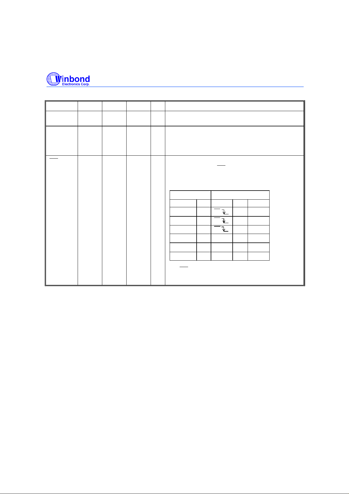
LOCK
LOCK
DP
SYMBOL 22-PIN 24-PIN 28-PIN I/O FUNCTION
(W91F810LN/
F810ALN/
F811ALN only)
W91F810N SERIES
6 6 7 I
The function of this terminal is to prevent "0"
dialing and "9" dialing under PABX system long
distance call control. When the first key input after
reset is 0 or 9, all key inputs, including the 0 or 9
key, become invalid and the chip generates no
output. The telephone is reinitialized by a reset.
The function of the
pin is shown below:
H/P MUTE 7 7 8 I
13 15 18 O
DTMF 14 16 19 O
LOCK PIN
V
DD
Floating
V
SS
FUNCTION
"0", "9" dialing inhibited
Normal dialing Mode
"0" dialing inhibited
The H/P MUTE is a conventional inverter output.
During pulse dialing, flash break or hold period, this
output is active high; otherwise, it remains in low
state.
N-channel open drain dialing pulse output.
Flash key will cause DP to be active in either tone
mode or pulse mode.
The timing diagram for pulse mode is shown in
Figure 1(a, b).
During pulse dialing, this pin remains in a low state
regardless of the keypad input. In tone mode, it will
output a dual or single tone.
A detailed timing diagram for tone mode is shown in
Figure 2(a, b).
OUTPUT FREQUENCY
R1
R2
R3
R4
C1
C2
C3
Specified
697
770
852
941
1209
1336
1477
Actual
699
766
848
948
1216
1332
1472
Error %
+0.28
-0.52
-0.47
+0.74
+0.57
-0.30
-0.34
- 4 -
W91F810N SERIES
HFI
HFI
HFI
Pin Description, continued
SYMBOL 22-PIN 24-PIN 28-PIN I/O FUNCTION
VDD, VSS 16, 8 18, 8 21, 9 I
V1, V2 - - 14, 15 O Volume control output pins. These two pins can be
, HFO
- 12, 13 13, 16 I, O Handfree control pins.
Power input pins for the dialer chip. VDD is the power
and VSS is the ground.
toggled by the volume control keys (Vup, Vdown).
These two pins output is a conventional CMOS Nchannel open drain output.
A low pulse on the
input pin toggles the
handfree control state. The status of the handfree
control state is listed in the following table:
CURRENT STATE NEXT STATE
HOOK SW.
On Hook
Off Hook
On Hook
Off Hook
Off Hook
HFO
Low
High
High
-
Low
High
INPUT
HFI
HFI
HFI
Off Hook
On Hook
On Hook
HFO
High
Low
Low
Low
Low
High
DIALING
Yes
No
Yes
Yes
No
Yes
The
pin is pulled to VDD by an internal resistor.
A detailed timing diagram is shown in Figure 3.
Publication Release Date: March 2000
- 5 - Revision A2
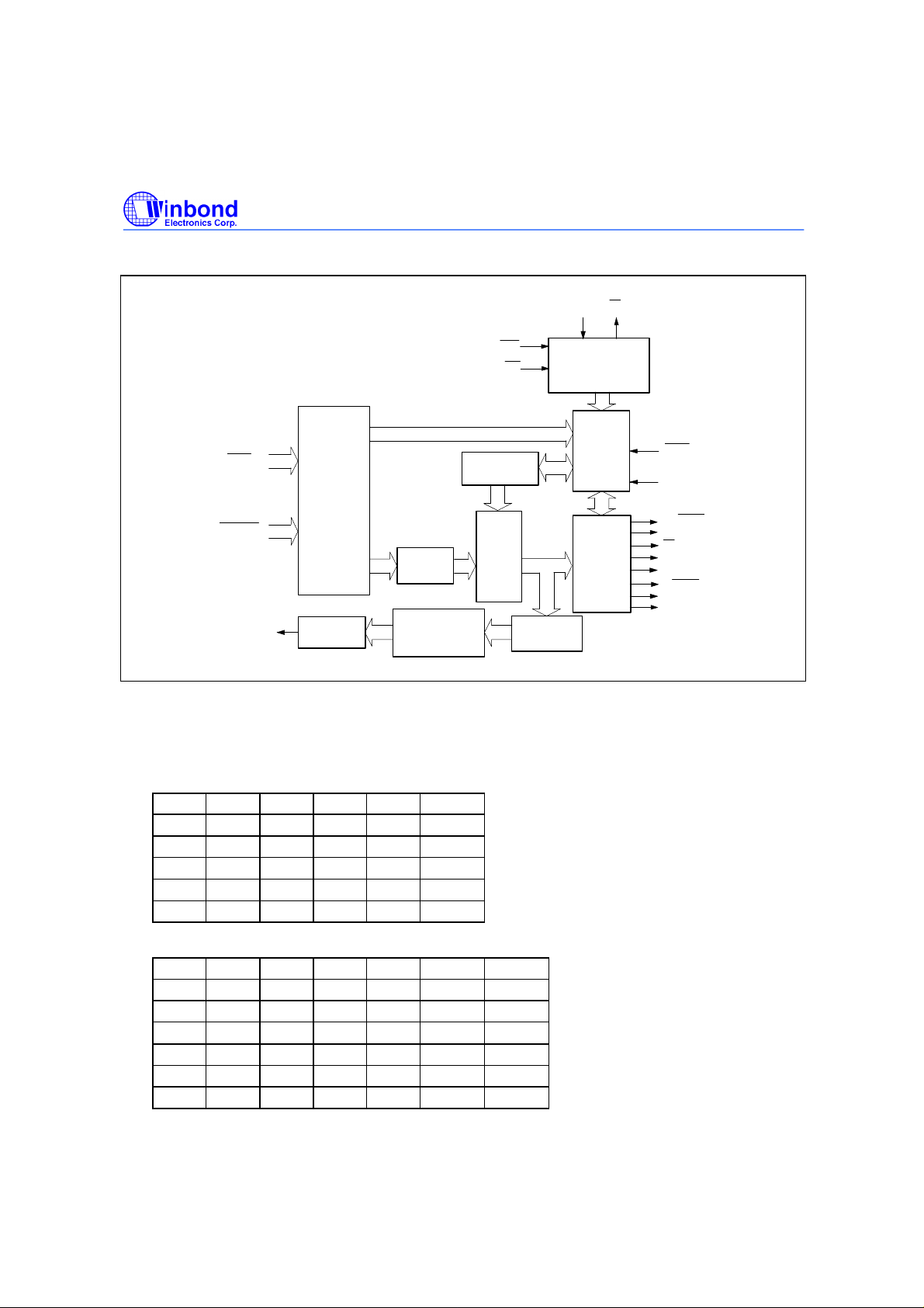
BLOCK DIAGRAM
W91F810N SERIES
XT XT
ROW
(R1 ~ R7)
COLUMN
(C1 ~ C6)
DTMF
KEYBOARD
INTERFACE
D/A
CONVERTER
LOCATION
LATCH
ROW & COLUMN
PROGRAMMABLE
COUNTER
HKS
HFI
READ/WRITE
COUNTER
RAM
DATA LATCH
& DECODER
SYSTEM CLOCK
GENERATOR
CONTROL
LOGIC
PULSE
CONTROL
LOGIC
LOCK
MODE
T/P MUTE
KT
DP
HFO
H/P MUTE
K MUTE
V1
V2
FUNCTIONAL DESCRIPTION
Keyboard Operation
C1 C2 C3 C4 C5 VSS
1 2 3 S M0 EM1 R1
4 5 6 F4 M1 EM2 R2
7 8 9 Page M2 EM3 R3
*/
T
F1 F2 F3 H M4 VX/R5
M5 M6 M7 M8 M9 MUTE R6
C1 C2 C3 C4 C5 C6 VSS
1 2 3 S M0 M10 EM1 R1
4 5 6 F4 M1 M11 EM2 R2
7 8 9 Page M2 M12 EM3 R3
*/
T
F1 F2 F3 H M4 M14 Vx/R5
M5 M6 M7 M8 M9 R MUTE R6
M15 M16 M17 M18 M19 Vup Vdown R7
• S: Store function key
0 # R/P M3 SAVE R4
0 # R/P M3 M13 SAVE R4
- 6 -
W91F810N SERIES
HFI
HFI
HFI
HFI
• Page: Indirect repertory memory dialing function key
• H: Hold function key
• R: One key redial function key
• R/P: Redial and pause function key
• */T: * in tone mode and P
• SAVE: Save function key for one-touch 32-digit memory
• MUTE: Mute function key for speech mute
−
• M0
M9: One touch memory. The dialing number can be stored in M0−M9 locations by the S key.
Note that the two touch memory (Page+ 0... Page+9) share the same memory buffer with
M10−M19, respectively
• M10, ..., M19: One touch or two touch memory keys. If there are no M10
Page+(M0−M9) can be used to simulate M10−M19.
• EM1, ..., EM3: Emergency one-touch memory key
• A: Indirect repertory dialing function key
• F1, ..., F4: Flash function keys: F1 = 600 mS, F2 = 300 mS, F3 = 73 mS, F4 = 100 mS; all flash
pause time is 1.0 S
→
T key in pulse mode
−
M19 keys,
Note: D1, ..., Dn, D1`, ..., Dn`, */T, #, Mm: M0, ..., M9, Mn: M0, ..., M19, Ln: 0−9
PAGE + LN = PAGE + Mm = M10−M19
Normal Dialing
OFF HOOK (or ON HOOK &
1. D1, D2, …, Dn will be dialed out.
2. Dialing length is unlimited, but redial is inhibited if length oversteps 32 digits in normal dialing.
), D1 , D2
, …,
Dn
Redialing Dialing
1. OFF HOOK (or ON HOOK &
Come ON HOOK , OFF HOOK (or ON HOOK &
The R/P key can execute redial function only as first key-in after off-hook. Otherwise, it will invoke
the pause function.
2. OFF HOOK (or ON HOOK &
a. The one-key redial function timing diagram is shown in Figure 5.
b. If dialing of D1 to Dn is finished, pressing R key will cause the pulse output pin to
go low for 2.2 seconds break time and a 600ms pause will automatically be added.
, D1 , D2
, …,
), R/P
), D1 , D2 , ..., Dn , R
Dn , BUSY
Publication Release Date: March 2000
- 7 - Revision A2
W91F810N SERIES
HFI
HFI
or
HFI
or
HFI
HFI
HFI
c. If the pulses of the dialed number D1
3. OFF HOOK (or ON HOOK &
come, OFF HOOK , OKR (or R/P )
to
Dn have not finished, R will be ignored.
), D1 , D2 , ..., Dn , Busy ON HOOK
If R is the first key after OFF HOOK, it only can execute the redialing function but will not cause
the pulse output pin to go low for the break time of 2.2 seconds.
Number Store
1. OFF HOOK (or ON HOOK &
Mn (or PAGE , Ln or EMn or SAVE
), D1 , D2 , ..., Dn , S , S ,
PAGE , Mm )
a. The dialing out of D1 to Dn must first be finished before the S key is pressed.
b. D1, D2, …, Dn will be stored in memory location Mn or saved and then dialed out.
2. OFF HOOK (or ON HOOK &
Mn (or Ln or EMn or SAVE
), S , D1 , D2 , ..., Dn , S ,
PAGE , Mm )
a. D1, D2, …, Dn will be stored in memory location, Mn (or saved), but will not be dialed out.
b. R/P and */T keys can be stored as a digit in memory, but the R/P key cannot be the
first digit. In store mode, R/P is the pause function key.
c. The store mode is released after the store function is executed or when the state of the hook
switch changes or the flash function is executed.
Save
OFF HOOK (or ON HOOK &
a. D1, D2, ..., Dn will be dialed out.
b. If the dialing of D1 to Dn is finished, pressing SAVE will duplicate D1 to Dn to the save
memory.
OFF HOOK (or ON HOOK &
come on OFF HOOK (or ON HOOK &
c. D1 to Dn will be dialed out after the SAVE key is pressed.
), D1 , D2 , ..., Dn , SAVE
),
), SAVE
- 8 -
 Loading...