

Winbond Electronics W91541LN, W91541ALN, W91540N, W91540AN, W91544AN Datasheet
...
W91540N SERIES
DP
10-MEMORY TONE/PULSE DIALER WITH SAVE,
KEYTONE, LOCK, AND HANDFREE FUNCTIONS
GENERAL DESCRIPTION
The W91540N series are tone/pulse switchable telephone dialers with 10 memories, keytone or lock
function, and handfree dialing control. These chips are fabricated using Winbond's high-performance
CMOS technology and thus offer good performance in low-voltage and low-power operations.
FEATURES
• DTMF/pulse switchable dialer
• Two by 32-digit redial and save memory
• Ten by 16 digit two-touch indirect repertory memory
• Pulse-to-tone (*/T) keypad for long distance call operation
• Cascaded dialing
• Uses 5 × 5 keyboard
• Easy operation with redial, flash, pause, and */T keypads
• Pause, P→T (pulse-to-tone) can be stored as a digit in memory
• 0 or 9 dialing inhibition pin for PABX system or long distance dialing lock out
• Dialing rate (10 ppS or 20 ppS) selected by bonding option
• Minimum tone output duration: 93 mS (W91544AN: 87 mS)
• Minimum intertone pause: 93 mS (W91544AN: 87 mS)
• Pause time: 3.6 sec
• 300 mS off-hook delay in lock mode (
• Flash break time (73 mS, 100 mS, 300 mS, or 600 mS) selectable by keypad; pause time is 1.0 S
• Make/break ratio (2:3 or 1:2) selectable by Mode pin
• Key tone output for valid keypad entry recognition
• On-chip power-on reset
• Uses 3.579545 MHz crystal or ceramic resonator
• Packaged in 18 or 20-pin DIP
remains low for 300 mS while off-hook)
Publication Release Date: May 1997
- 1 - Revision A2
W91540N SERIES
DP/C5
C1
• The different dialers in the W91540N series are shown in the following table:
TYPE NO. REPLACEMENT
TYPE NO.
PULSE
(ppS)
FLASH
(mS)
M/B KEY
TONE
HANDFREE
DIALING
LOCK PACKAGE
W91540N W91540 10 600/300/73/100 Pin Yes - - 18
W91541
W91540AN W91540A 10 600/300/73/100 Pin Yes Yes - 20
W91541A
W91541LN W91541L 10 600/300/73/100 Pin - - Yes 18
W91541ALN W91541AL 10 600/300/73/100 Pin - Yes Yes 20
W91542N W91542 20 600/300/73/100 Pin Yes - - 18
W91542AN W91542A 20 600/300/73/100 Pin Yes Yes - 20
W91544AN New type 10 600/300/73/100 Pin Yes Yes - 20
Note: The W91544AN is designed specifically for use in France. The pause time is not added in pulse-to-tone mode.
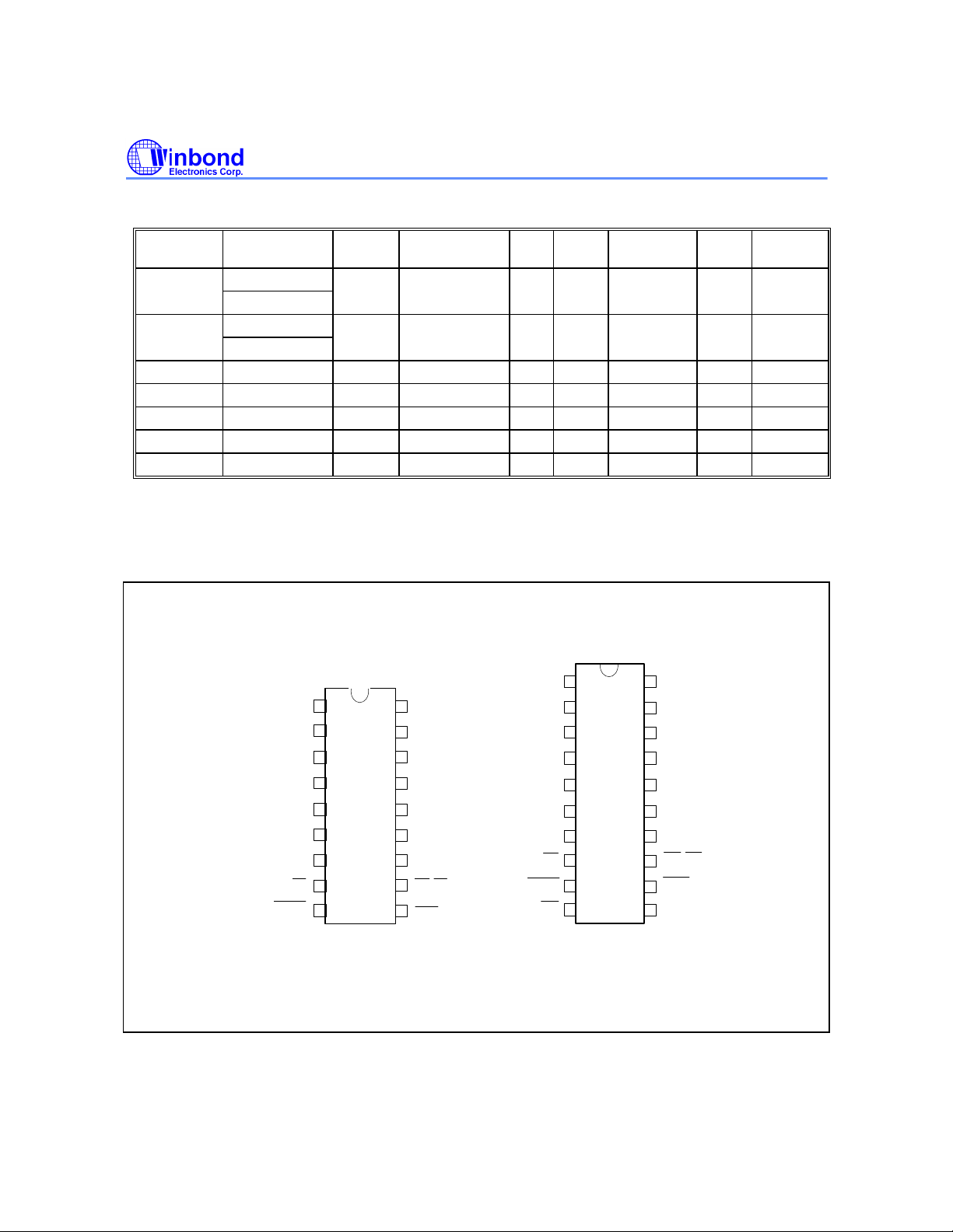
PIN CONFIGURATIONS
20
19
18
17
16
15
14
13
12
11
R4
R3
R2
R1
V
DD
MODE
DTMF
DP/C5
HKS
HFO
C1
C2
C3
C4
KT
V
SS
XT
XT
T/P MUTE
1
18
16
15
14
13
12
11
10
17
R4
R3
R2
R1
V
DD
MODE
DTMF
HKS
1
2
3
4
5
6
7
8
9
C2
C3
C4
KT
V
SS
XT
XT
T/P MUTE
HFI
2
3
4
5
6
7
8
9
10
(PINS)
W91540N/542N
W91540AN/542AN/544AN
- 2 -
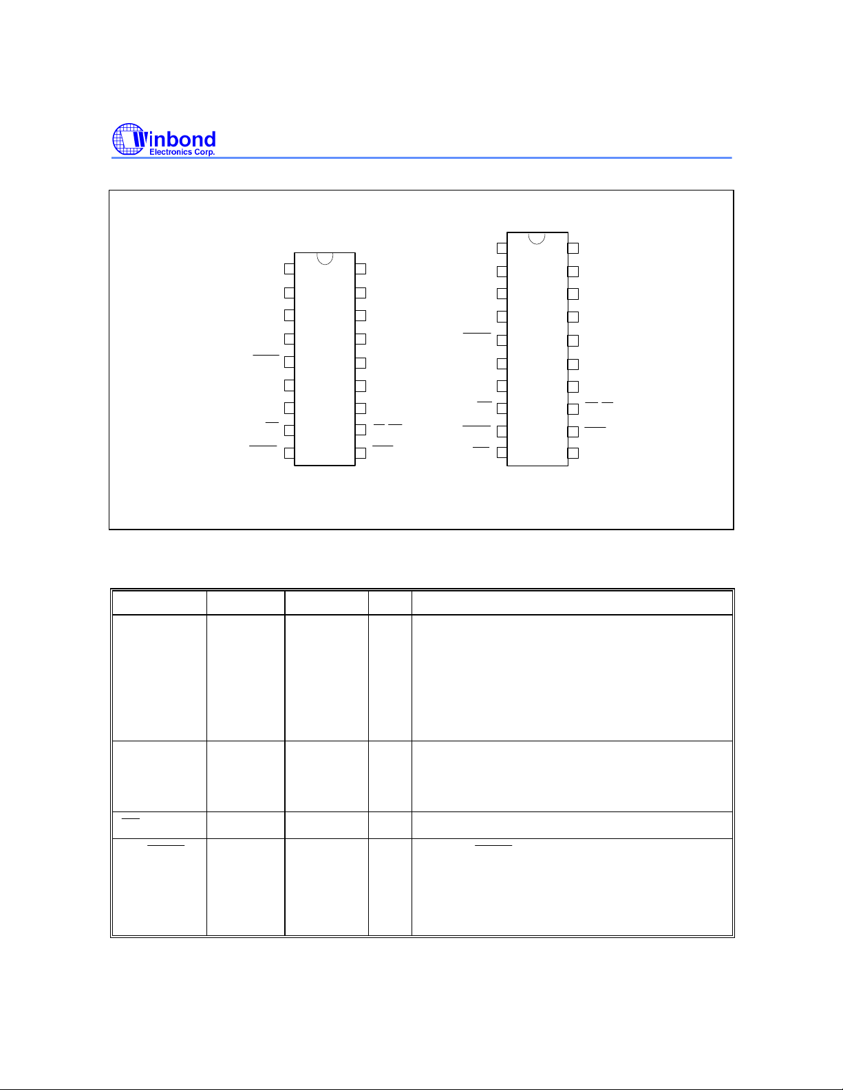
Pin Configurations, continued
XT
MUTE
MUTE
T/P MUTE
C1
C2
C3
C4
LOCK
V
SS
XT
XT
1
2
3
4
5
6
7
8
9 10
18
17
16
15
14
13
12
11
R4
R3
R2
R1
V
DD
MODE
DTMF
DP/C5
HKS
C1
C2
C3
C4
LOCK
VSS
XT
XT
T/P MUTE
HFI
W91540N SERIES
1
20
R4
19
18
17
16
15
14
13
12
11
R3
R2
R1
V
DD
MODE
DTMF
DP/C5
HKS
HFO
2
3
4
5
6
7
8
9
10
W91541LN
W91541ALN
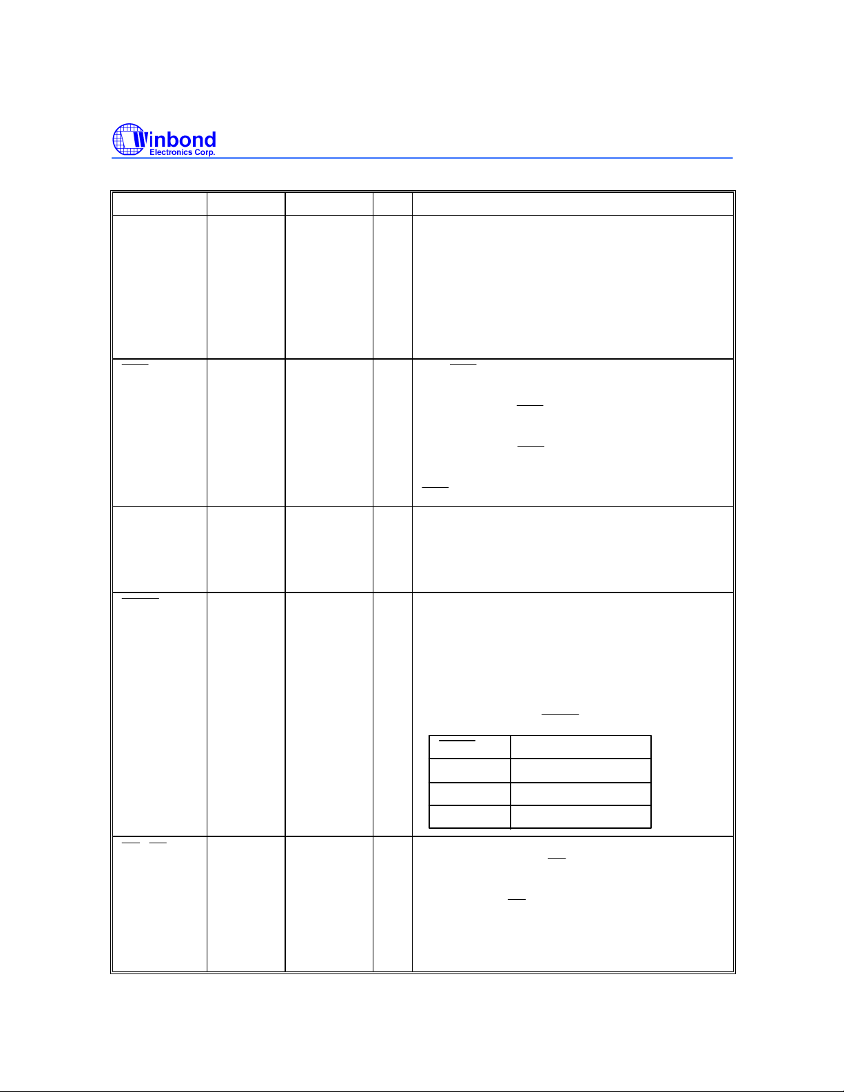
PIN DESCRIPTION
SYMBOL 18-PIN 20-PIN I/O FUNCTION
Column-Row
Inputs
1−4
&
15−18
1−4
&
17−20
XT 7 7 I A built-in inverter provides oscillation with an
8 8 O Crystal oscillator output pin.
T/P
9 9 O
I The keyboard input is compatible with a standard
5 × 5 keyboard, an inexpensive single contact
(Form A) keyboard, and electronic input.
In normal operation, any single button can be
pushed to produce a dual tone, pulses, or a
function. Activation of two or more buttons will
result in no response except for single tone.
inexpensive 3.579545 MHz crystal. The oscillator
ceases when a keypad input is not sensed. The
crystal frequency deviation is 0.02%.
The T/P
is a conventional CMOS N-
channel open drain output.
The output transistor is switched on low level
during dialing sequence (both pulse and tone
mode). Otherwise, it is switched off.
Publication Release Date: May 1997
- 3 - Revision A2
W91540N SERIES
HKS
HKS
HKS
HKS
HKS
LOCK
LOCK
DP/C5
Pin Description, continued
SYMBOL 18-PIN 20-PIN I/O FUNCTION
MODE 13 15 I Pulling mode pin to VSS places dialer in tone
mode.
Pulling mode pin to VDD places dialer in pulse
mode with M/B ratio of 40:60 (10 ppS, except for
W91542N/542AN is 20 ppS).
Leaving mode pin floating places dialer in pulse
mode with M/B ratio of 33.3:66.7 (10 ppS, except
for W91542N/542AN is 20 ppS).
10 12 I
The
(hook switch) input is used to sense
whether the handset is on-hook or off-hook.
KT 5
(except for
W91541LN)
(only for
W91541LN)
11 13 O N-channel open drain dialing pulse output.
On-hook state,
= 1: chip is in sleeping
mode, no operation.
Off-hook state,
= 0: chip is enabled for
normal operation.
pin is pulled to VDD by an internal resistor.
5
(except for
W91541ALN)
O The key tone output is a conventional CMOS
inverter. The key tone is generated when any
valid key is pressed; the KT pin generates a 1.2
KHz square wave at 35 mS. When no key is
pressed, the KT pin remains in low state.
5
5
(only for
W91541ALN)
I The function of this terminal is to prevent "0"
dialing and "9" dialing under PABX system long
distance call control. When the first key input
after reset is 0 or 9, all key inputs, including the 0
or 9 key, become invalid and the chip generates
no output. The telephone is reinitialized by a
reset.
The function of the
LOCK PIN
V
DD
Floating
V
SS
"0", "9" dialing inhibited
Normal dialing
"0" dialing inhibited
pin is shown below:
FUNCTION
Flash key will cause DP to be active in either
tone mode or pulse mode.
In lock mode, DP remains low for 300 mS during
off-hook delay time.
The timing diagram for pulse mode is shown in
Figure 1(a, b, c, d).
- 4 -
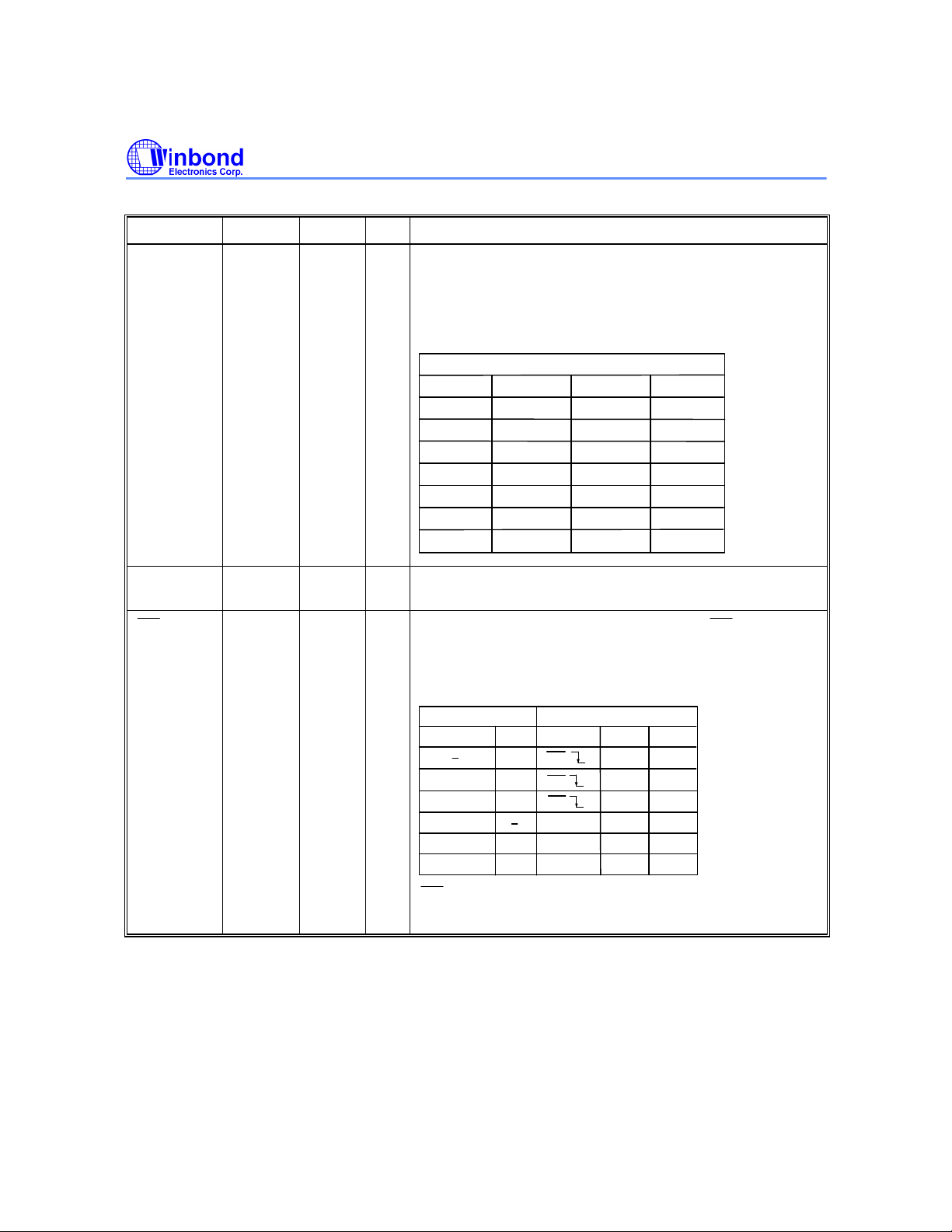
W91540N SERIES
HFI
HFI
HFI
HFI
Pin Description, continued
SYMBOL 18-PIN 20-PIN I/O FUNCTION
DTMF 12 14 O During pulse dialing, this pin remains in low state
regardless of keypad input. In tone mode, it will output a
dual or single tone.
A detailed timing diagram for tone mode is shown in
Figure 2(a, b, c, d)
OUTPUT FREQUENCY
R1
R2
R3
R4
C1
C2
C3
Specified
697
770
852
941
1209
1336
1477
Actual
699
766
848
948
1216
1332
1472
Error %
+0.28
-0.52
-0.47
+0.74
+0.57
-0.30
-0.34
VDD, VSS 14, 6 16, 6 I Power input pins for the dialer chip. VDD is the main
power and VSS is the ground.
, HFO
- 10, 11 I, O
Handfree control pins. A low pulse on the
input pin
toggles the handfree control state.
Status of the handfree control is listed in the following
table:
Input
HFI
HFI
NEXT STATE
HFO
High
Low
Low Yes
Low Yes
Dialing
Yes
No
Yes
CURRENT STATE
Hook SW.
On Hook High
Off Hook
On Hook Off Hook
Off Hook
Off Hook High On Hook High
HFO
Low
High
Low On Hook Low No
pin is pulled to VDD by an internal resistor.
Detailed timing diagram is shown in Figure 3.
Publication Release Date: May 1997
- 5 - Revision A2
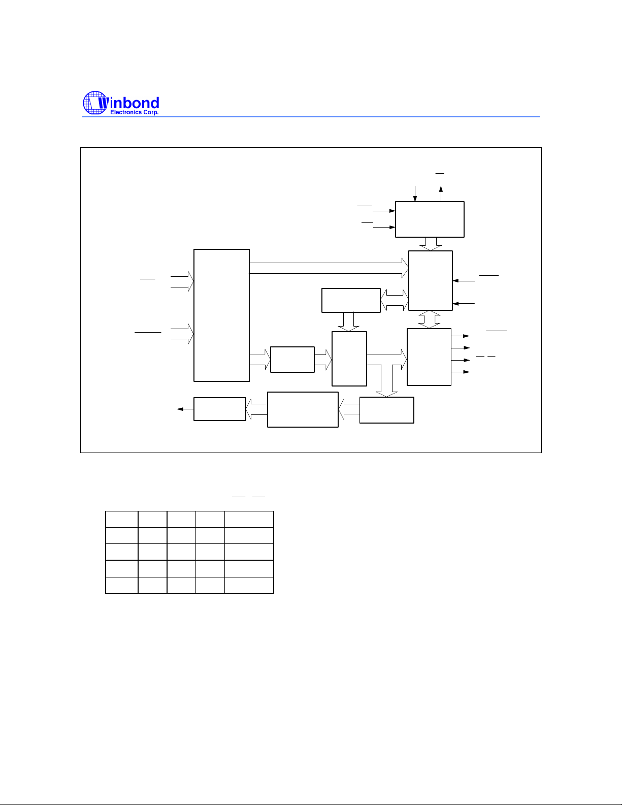
BLOCK DIAGRAM
DP/C5
W91540N SERIES
XT XT
ROW
(R1 to R4, Vx)
KEYBOARD
INTERFACE
COLUMN
(C1 to C4)
DTMF
D/A
CONVERTER
FUNCTIONAL DESCRIPTION
C1 C2 C3 C4
LOCATION
LATCH
ROW & COLUMN
PROGRAMMABLE
COUNTER
HKS
HFI
READ/WRITE
COUNTER
RAM
DATA LATCH
& DECODER
SYSTEM CLOCK
GENERATOR
CONTROL
LOGIC
PULSE
CONTROL
LOGIC
LOCK
MODE
T/P MUTE
KT
DP/C5
HFO
1 2 3 S R1
4 5 6 F4 R2
7 8 9 A R3
∗/T
0 # R/P SAVE R4
F1 F2 F3 Vx
• S: Store function key
• A: Indirect repertory memory dialing function key
• R/P: Redial and pause function key
• ∗/T: ∗ in tone mode and P→T in pulse mode
• SAVE: Save function key for one-touch 32-digit memory
• F1, ..., F4: Flash function keys; F1 = 600 mS, F2 = 300 mS, F3 = 73 mS, F4 = 100 mS, and flash
pause time for each key is 1.0 mS
Note: Ln = 0, ..., 9; Dn = 0, ..., 9, */T, #, Pause.
- 6 -
 Loading...