

Winbond Electronics W91433N, W91432N Datasheet
W91430N SERIES
13-MEMORY TONE/PULSE DIALER
WITH SAVE FUNCTION
GENERAL DESCRIPTION
The W91430N series are Si-gate CMOS ICs that provide the necessary signals for either tone or
pulse dialing. The W91430N series features save memory and a 13 by 16 digit automatic dialing
memory.
FEATURES
• DTMF/pulse switchable dialer
• Two by 32 digit redial and save memory
• Three by 16 digit one-touch direct memory
• Ten
by 16 digit two-touch direct memory
• Redial memory cascadable with normal dialing; dialing length is unlimited, but if length oversteps
32-digit the redial function is inhibited
•
Pulse-to-tone (*/T) keypad for long distance call operation
•
Uses 5 × 5 keyboard
•
Easy operation with redial, flash, pause and */T keypads
•
Flash, pause, P→T (Pulse-to-tone) can be stored as a digit in memory
•
Dialing rate (10, 20 ppS ) selected by bonding option
• On hook debounce time: 150 msec.
•
Minimum tone output duration: 93 msec.
•
Minimum intertone pause: 93 msec.
•
Flash break time (73, 100, 300, 600 msec.) selectable by keypad; pause time is 1 sec.
•
On-chip power-on reset
•
Uses 3.579545 MHz crystal or ceramic resonator
•
Packaged in 18-pin plastic DIP
• The different dialers in the W91430N series are shown in the following table:
TYPE NO. REPLACEMENT
TYPE NO.
PULSE
(ppS)
FLASH
(mS)
PAUSE
(S)
M/B
W91432N W91432 10 600/300/73/100 3.6 Pin
W91444
W91446
W91447
W91445
W91434G
W91435G
W91433N W91433 20 600/300/73/100 3.6 Pin
Publication Release Date: May 1997
- 1 - Revision A3
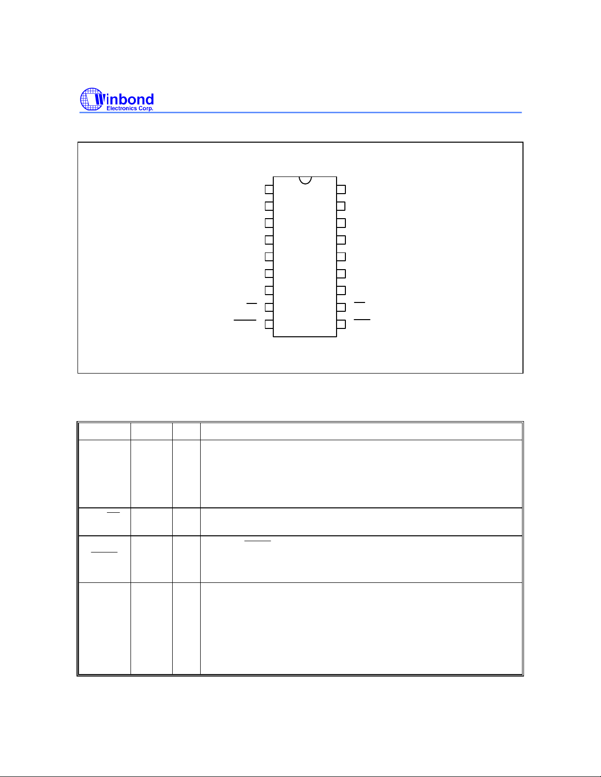
PIN CONFIGURATION
XT
XT1234
7
8
9
HKS
DTMF
MODE
R4R3R2
R1
12
18
16
15
14
10
11
13
XT
MUTE
MUTE
W91430N SERIES
C1
C2
C3
C4
C5
V
SS
T/P MUTE
5
6
17
V
DP
DD
PIN DESCRIPTION
SYMBOL PIN I/O FUNCTION
Column-
Row
Inputs
1−5
&
15−18
The keyboard inputs may be used with either a standard 5 × 5
keyboard or an inexpensive single contact (Form A) keyborad.
I
Electronic input from a µC can also be used.
A valid key in is defined as a single row being connected to a single
column.
XT,
7, 8 I, O A built-in inverter provides oscillation with an inexpensive 3.579545
MHz crystal or ceramic resonator.
T/P
9 O
The T/P
is a conventional CMOS N-channel open drain output.
The output transistor is switched on during dialing sequence and flash
break time. Otherwise, it is switched off.
MODE 13 I Pulling mode pin to VSS places the dialer in tone mode.
Pulling mode pin to VDD places the dialer in pulse mode with M/B ratio
40:60
(20 ppS only for W91433N and 10 ppS for the others, M/B = 40:60).
Floating mode pin places the dialer in pulse mode with M/B ratio 33:67
(20 ppS only for W91433N and 10 ppS for the others).
- 2 -
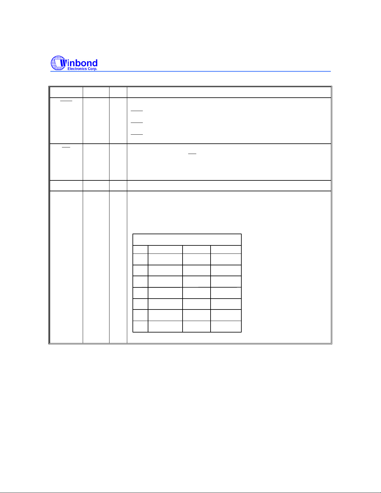
W91430N SERIES
HKS
HKS
HKS
HKS
DP
R1R2R3
R4
C1
C2
C3
Pin Description, continued
SYMBOL PIN I/O FUNCTION
10 I Hook switch input.
= VDD: On-hook state. Chip in sleeping mode, no operation.
= VSS: Off-hook state. Chip is enabled for normal operation.
pin is pulled to VDD by internal resistor.
11 O N-channel open drain dialing pulse output.
Flash key will cause DP to be active in either tone mode or pulse
mode.
The timing diagram in pulse mode is shown in Figure 1(a, b, c).
VDD, VSS 14, 6 I Power input pins.
DTMF 12 O In pulse mode, this pin remains in low state at all time.
In the tone mode, it will output a dual or single tone.
Detailed timing diagram for tone mode is shown in
Figure 2(a, b, c).
Output Frequency
Specified Actual Error %
697
770
852
941
1209
1336
1477
699
766
848
948
1216
1332
1472
+0.28
-0.52
-0.47
+0.74
+0.57
-0.30
-0.34
Publication Release Date: May 1997
- 3 - Revision A3
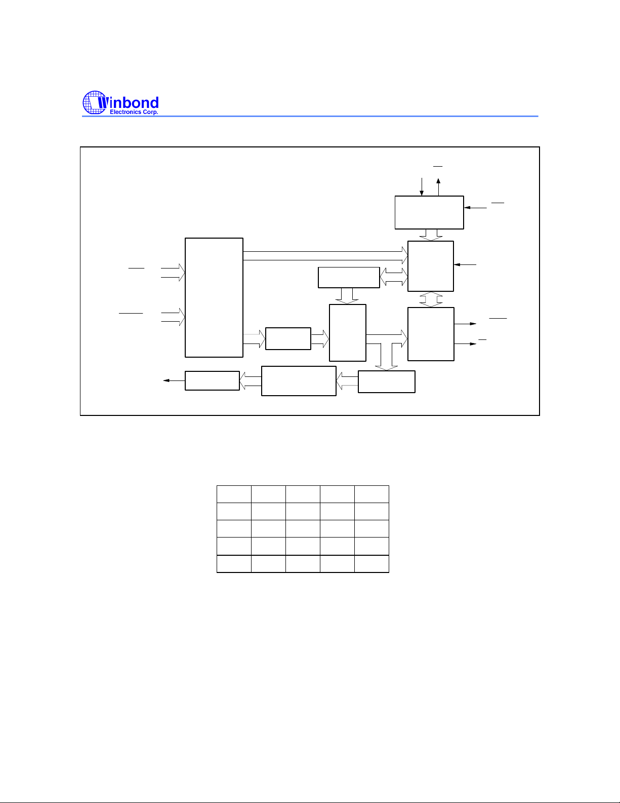
BLOCK DIAGRAM
W91430N SERIES
XT XT
ROW
(R1 to R4, Vx)
COLUMN
(C1 to C5)
DTMF
KEYBOARD
INTERFACE
D/A
CONVERTER
FUNCTIONAL DESCRIPTION
Keyboard Operation
C1 C2 C3 C4 C5
1 2 3 S M1 R1
LOCATION
LATCH
ROW & COLUMN
PROGRAMMABLE
COUNTER
READ/WRITE
COUNTER
RAM
DATA LATCH
& DECODER
SYSTEM CLOCK
GENERATOR
CONTROL
LOGIC
PULSE
CONTROL
LOGIC
HKS
MODE
T/P MUTE
DP
4 5 6 F4 M2 R2
7 8 9 A M3 R3
∗/T
0 # R/P SAVE R4
F1 F2 F3 VX
• S: Store function key
• A: Indirect repertory dialing function key
• R/P: Redial and pause function key
• SAVE: Save function key
• ∗/T: ∗ in tone mode and P→T in pulse mode
• M1 to M3: One-touch memory
• F1, ..., F4: Flash keys, F1 = 600 mS, F2 = 300 mS, F3 = 73 mS, F4 = 100 mS
Note: D1, ..., Dn, D1', ..., Dn': 0, ..., 9, */T, #; Mn: M1, ..., M3; Ln: 0, ..., 9 ; Fn: F1, ..., F4
- 4 -
W91430N SERIES
Normal Dialing
OFF HOOK , D1 , D2 , ..., Dn
1. D1, D2, …, Dn will be dialed out.
2. Dialing length is unlimited, but redial is inhibited if length oversteps 32 digits in normal dialing.
Redialing
OFF HOOK , D1 , D2 , ..., Dn Busy, Come ON HOOK , OFF HOOK , R/P
1. The redial memory content will be dialed out.
2. The R/P key can execute the redial function only as the first key-in after off-hook; otherwise,
it executes pause function.
3. If redialing length oversteps 32 digits, the redialing function will be inhibited.
Number Store
OFF HOOK , D1 , D2 , ..., Dn , S , S , Mn (or Ln )
1. If the sequence of the dialed digits D1, D2, ..., Dn has not
finished,
2. D1, D2, ..., Dn will be stored in memory location and dialed out.
OFF HOOK , S , D1 , D2 , ..., Dn , S , Mn (or Ln )
3. D1, D2, ..., Dn will be stored in memory location but will not be dialed out.
4. R/P and */T keys can be stored as a digit in memory.
In store mode, R/P is the pause function key; */T is the pulse to tone function key.
5. The store mode is released after the store function is executed or when the state of the hook
switch is changed.
S will be ignored.
Repertory Dialing
1. OFF HOOK , Mn
2. OFF HOOK , A , Ln
Access Pause
OFF HOOK , D1 , D2 , R/P , D3 , ..., Dn
1. The pause function can be stored as a digit in memory.
2. The pause function is executed in normal dialing, redial dialing, or memory dialing.
3. A detailed timing diagram for the pause function is shown in Figure 3.
Publication Release Date: May 1997
- 5 - Revision A3
 Loading...