

Winbond Electronics W89C840AF Datasheet

W89C840AF
Winbond LAN
W89C840AF
100/10Mbps Ethernet Controller
Publication Release Date:October 2000
-1 - Revision 1.01

W89C840AF
Publication Release Date:October 2000
-2 - Revision 1.01

W89C840AF
W89C840AF is a highly integrated Ethernet LAN controller for both 100BaseT and 10BaseT Ethernet.
It provides a host bus interface complying with the PCI local bus specification revision 2.1, and the MII
interface complying with the IEEE802.3u standard for easily implementing an Ethernet LAN adapter. The
built-in 2K bytes transmit FIFO and 4K bytes receive FIFO, controlled by the on-chip bus master, are designed
for improving network performance and reducing the host bus utilitzation.
The on-chip DMA controller handles the data transfer between the host memory and the FIFOs. The data
received from network are queued into the receive FIFO and then, directly moved into the host memory
through the PCI bus. On the other hand, the transmitted data are fetched from the host memory and directly
queued into the transmit FIFO. No extra on-board memory is needed for data buffering during the data
transceiving operation.
For featuring the specifications of PC97/98, W89C840AF implements power management functinos
which are compliant with Advanced Configuration and Power Interface ( ACPI) specification Rev. 1.0, PCI
Power Management Interface specification Rev. 1.0, and Network Device Class Power Management Reference
specification V1.0a as well as remote wakeup function based on the OnNow initiative and the ACPI
specification requirement of PC 97 and PC 98.
Many versatile registers, total 48 inside, including host bus control registers, direct memory
access(DMA) control registers, media access control registers(MAC), power management control/status
registers and signature identification registers, are implemented for system configuring and control. All of these
long word accessible registers perform the status report and the precisely control on the operation of transmit
and receive. It also provides an extra channel for the on-line application program to update the on-board
expansion ROM device in some specific application environment.
Features
l Complies with IEEE 802.3, 802.3u, ANSI 8802-3 and Ethernet standards
l Supports PCI bus master mode for DMA operation, fully complying with PCI 2.1 standard
l Compliant with APCI R1.0, PCI power management R1.0 and Network device Class Power
management Reference specification V1.0a
l Supports remote wakeup function
l Both half duplex and full duplex available for 10/100M operation
l Flexible data structure for host compatibility and system performance
l Supports 25 to 33 Mhz PCI clock speed
l Supports full MII management function
l Provides EEPROM and flash memory on-board programming function
l Supports both big and little endian byte ordering for descriptor and buffer
l Flexible address filtering modes
-- 64-bit hash-table and one perfect address
-- all multicast and promiscuous
l A boot ROM interface, capable of supporting up to 256KB
l Supports automatic loading configuration register
l Internal and external loopback mode for diagnostic
Publication Release Date:October 2000
-3 - Revision 1.01

l Single 5 volt power supply
36
37
38
35
34
33
32
31
30
29
28
27
26
25
24
23
22
21
20
19
18
17
16
15
14
13
12
11
10
l 128 pins PQFP package
Pin Assignment
98
97
96
102
101
100
95
W89C840AF
65
68
69
70
71
72
73
74
94
93
89
88
87
86
85
84
83
82
81
80
75
79
78
77
76
103
104
105
106
107
108
109
110
111
112
113
114
115
116
117
118
119
120
121
122
123
124
125
126
127
128
GND
MIRXD0
MIRXD1
MIRXD2
MIRXD3
VCC
GND
RMGWKU
INTAB
RSTB
PWGD
PCICLK
GND
GNTB
REQB
PMEB
VCC
GND
AD31
AD30
AD29
AD28
AD27
AD26
AD25
AD24
MIRXER
MIRXCLK
VCC
GND
3
2
1
MICOL99MICRS
MIRXDV
AD23
IDSEL
C_BEB3
5
4
6
VCC
GND
AD22
7
MIMDIO
AD20
AD21
9
8
VCC
VCC
GND
MIMDC
MITXD392MITXD291MITXD190MITXD0
MITXEN
GND
MITXCLK
W89C840AF
DEVSELB
TRDYB
IRDYB
FRAMEB
VCC
C_BEB2
GND
AD16
AD17
AD18
AD19
BTADD17
BTADD16
BTADD15
SERRB
PERRB
STOPB
BTADD14
BTADD13
BTADD12
VCC
C_BEB1
PAR
BTADD9
BTADD11
BTADD10
AD14
AD15
GND
VCC
GND
AD13
BTADD8
AD11
AD12
BTADD5
BTADD6
BTADD7
AD8
AD9
AD10
BTADD367BTADD266BTADD1
BTADD4
EEDO/BTADATA3
EEDI/BTADATA2
EECK/BTADATA1
VCC
AD7
GND
C_BEB0
BTADD0
GND
VCC
BTADATA7
BTADATA6
BTADATA5
BTADATA4
BTADATA0
GND
VCC
EECS
BTCSB
BTOEB
BTWEB
GND
VCC
AD0
AD1
AD2
AD3
AD4
AD5
AD6
64
63
62
61
60
59
58
57
56
55
54
53
52
51
50
49
48
47
46
45
44
43
42
41
40
39
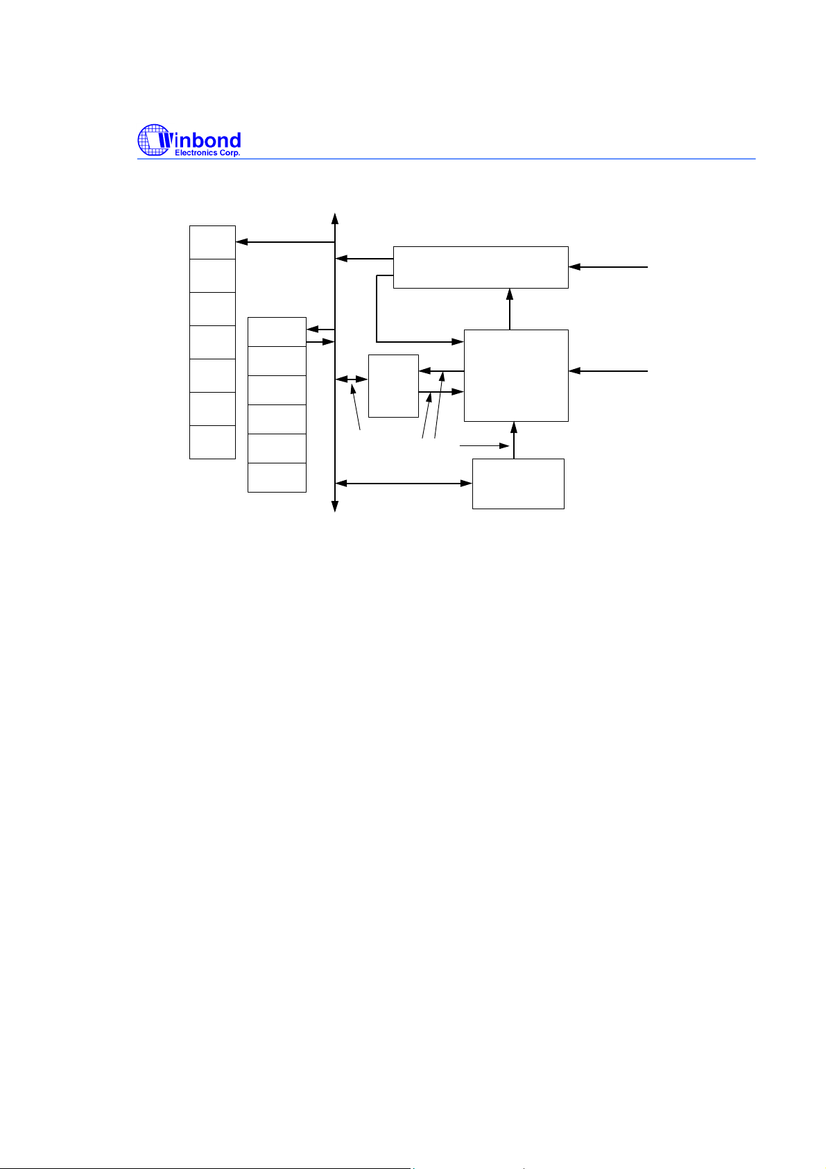
Fig 1: W89C840AF pin configuration
Publication Release Date:October 2000
-4 - Revision 1.01
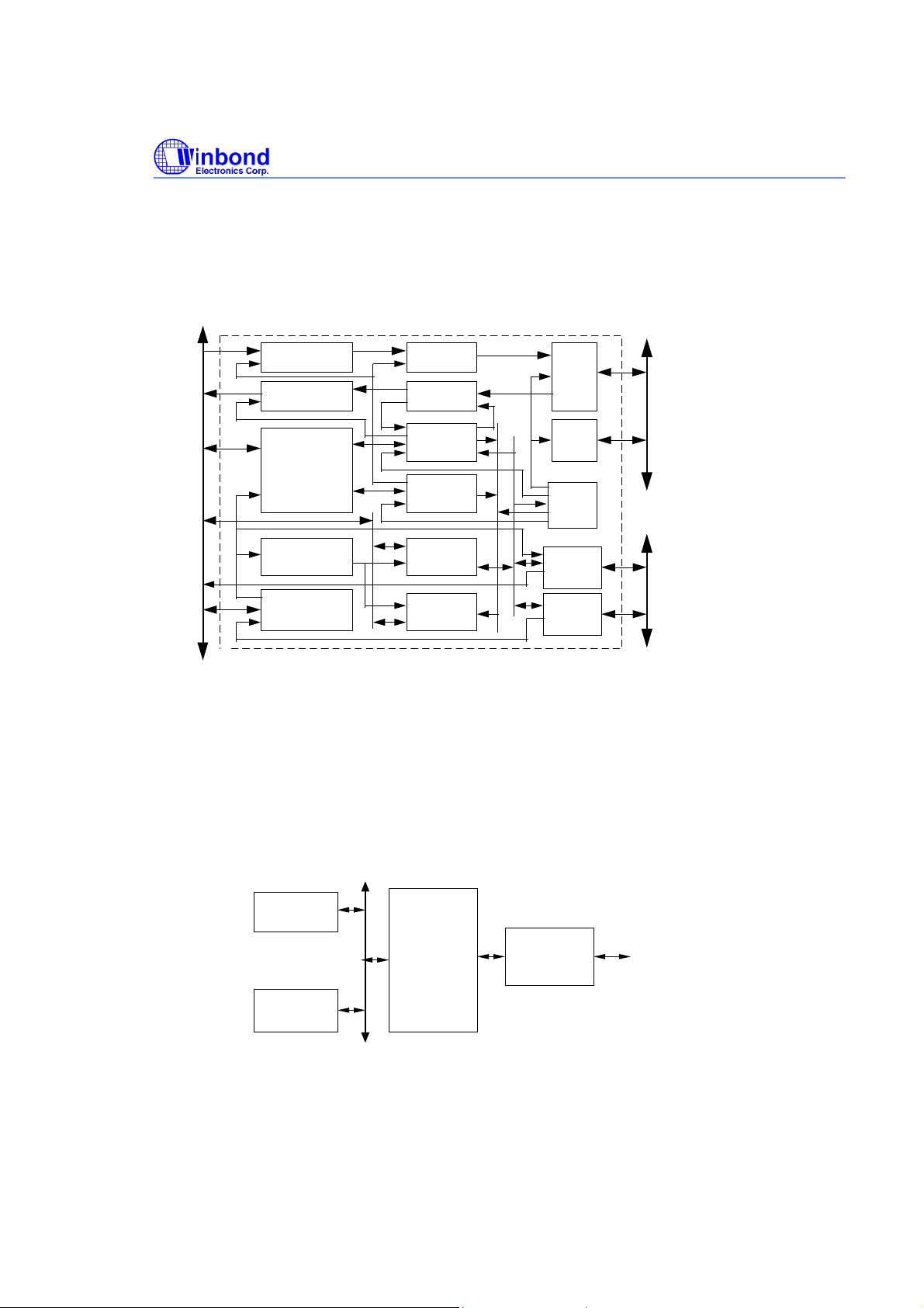
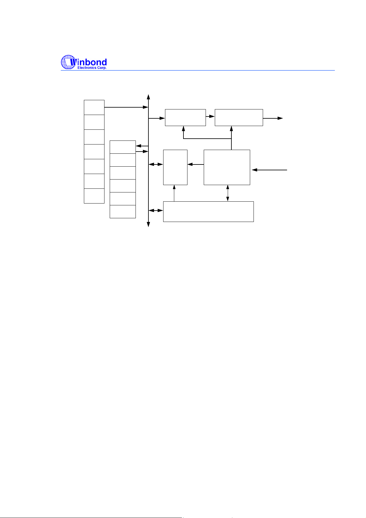
Block Diagram
W89C840AF
PCI
long word
aligning buffer
PCI interface
data driver
PCI bus
master
PCI bus slave
controller
configuration
registers
TX FIFO
RX FIFO
receive data
DMA machine
transmit data
DMA machine
control
registers
status
registers
MII
data
buffer
MII
control
signals
Media
Access
Controller
Expansion
ROM
interface
EEPROM
access
interface
Fig. 2 W89C840AF Block Diagram
MII
memory
interface
System Diagram
System
Memory
Physical layer
W89C840AF
Controller &
Transceiver
Media
Host
Controller
W89C840AF Typical Application
Fig. 3
Publication Release Date:October 2000
-5 - Revision 1.01

beginning and duration of a bus access. This signal
Pin Descriptions
1) PCI Interface
W89C840AF
Signal Name Pin
Type
PCICLK I 114 PCI Clock Input:
RSTB I 112 PCI Hardware reset signal:
AD[31:0] IO/TS 121-128,
C_BEB[3:0] IO/TS 3,15,24,
Pin
Number
5-12,
27-34,
38-45
35
Pin Description
W89C840AF supports PCI clock rate ranged from
25Mhz to 33MHz continuously. All PCI signals except
RST# and INTA#, are referenced on the rising edge of
this clock.
When asserted(active low), all PCI output pins of
W89C840AF will be in high impedance state, and all
open drain signals will be floated. The configurations
inside W89C840AF will be in its initial state. This
signal must be asserted for a period of at least 10 PCI
clocks to correctly take effect of a reset on hardware.
PCI Multiplexed Address and Data bus:
During the first cycle that FRAME# asserts, they act as
an address bus; on the other cycles, they are switched to
be a data bus.
Multiplexed command and byte enables:
These signals are driven by current bus master. During
address phase, they mean a bus command; on the other
phase, they present the byte enable of the transaction.
PAR IO/TS 23 Parity signal.
FRAMEB IO/STS 16 PCI Cycle Frame:
Publication Release Date:October 2000
-6 - Revision 1.01
This PAR represents the even parity across AD[31:0]
and C_BEB[3:0]. It has the same timing as AD[31:0]
but is delayed by one clock.
The current bus master asserts FRAMEB to indicate the
keeps asserted while the current transaction is ongoing
and keeps deasserted to indicate that the next data
phase is the final data phase.

IRDYB IO/STS 17 Initiator Ready:
The IRDYB is asserted by the current initiator to
indicate the ability to complete the data transfer at the
current data phase. The initiator asserts IRDYB to
indicate the valid write data, or to indicate it is ready to
accept the read data. More than or exactly one wait state
will be inserted if IRDYB is deasserted during the
current transaction. Data is transferred at the clock
rising edge when both IRDYB and TRDYB are asserted
at the same time.
TRDYB IO/STS 18 Target Ready:
Asserted by the current target to indicate ability to
complete data transfer at the current data phase. When
W89C840AF is operating at the bus slave mode, it
asserts TRDYB to indicate that the valid read data
presents on the bus or to indicate it is ready to accept
data. Wait states will be inserted if TRDYB is
deasserted. Data is transferred at the rising edge of the
PCI clock when IRDYB and TRDYB are both asserted
at the same time.
W89C840AF
STOPB IO/STS 20 PCI Stop:
Asserted by the current target to request PCI bus master
to stop the current transaction.
IDSEL I 4 PCI Initialization Device Select:
Asserted by host to signal the configuration access
request to W89C840AF.
DEVSELB IO/STS 19 PCI Device Select:
Asserted by the current target to indicate that it has
finished decoding its address as the current access
target. When W89C840AF is the current master, it
checks if the target asserted this signal within 5 PCI
clocks after having issued command. If not,
W89C840AF will abort the access operation, releases
PCI bus access right and acts no more bus master. When
W89C840AF is the target, it asserts DEVSELB in a
medium speed, i.e., within 2 clocks.
REQB O/TS 117 PCI Request:
Asserted by W89C840AF to request bus ownership.
REQB will be tri-stated when RSTB asserted.
GNTB I/TS 116 PCI Grant:
Asserted by host to grant that W89C840AF have got the
bus ownership. When RSTB asserted, W89C840AF will
ignore GNTB.
Publication Release Date:October 2000
-7 - Revision 1.01

PERRB IO/STS 21 PCI Parity Error:
Asserted by the current data receiptor. When
W89C840AF acts the bus master, if a data parity error
is detected and the parity error response bit (FCS<6>) is
also set, it will set both bits of FCS<24> and C14<13>
as 1 to terminate the current transaction after the
current data phase is finished. When W89C840AF acts
the target, if a data parity error is detected and the bit
FCS<6> is set, it will assert PERRB only.
SERRB O/OD 22 System Error:
This pin is asserted with one PCI clock width within
two PCI clocks after an address parity error is detected,
and keeps in high impedance state when idle.
The interrupt function caused by this event is gated by
the bits in FCS register.
W89C840AF will assert SERRB and will set a high to
the Detect Parity Error bit FCS<31> and the Signal
System Erro bit FCS<30> if an address parity error is
detected and SERRB enable bit FCS<8> is previously
set to 1.
The Bus Error Status bit C14<13> will be set to high if
both an address parity error is detected and the parity
error response bit FCS<6> is set to high.
W89C840AF
INTAB O/OD 111 Interrupt A:
INTAB is asserted when any one of unmasked interrupt
bits in C14/CISR is set. It keeps asserted until all of the
unmasked interrupt bits is cleared.
2) Power Managment Interface
Symbol Pin Type
PWGD I 113 Power Good
PMEB O/OD 118 Power Management Event
RMGWKU O/OD 110 Remote Magic Packet WakeUp
Pin
Number
Pin Description
When PWGD=1, W89C840A is put in normal operation
mode.
When PWGD=0, it isolates whole PCI bus except PMEB.
The PCI bus power can be off by operating system.
The PMEB signal indicates that a power management
event has occurred, i.e. there is a magic packet received in
suspend mode etc. This pin is open drain.
After received magic packet, this output signal
motherboard to execute wakeup process.
Publication Release Date:October 2000
-8 - Revision 1.01

2) BootROM and EEPROM Interface
W89C840AF
Signal Name Pin Type Pin
Number
BtAdd[17:0] O 83-75,72-
64
BtAdata[7:4] I/O 61-58 BootROM data bits 4 - 7
BtAdata[3]/EEDO I/O 57 EEPROM data output; BootROM data bit 3
BtAdata[2]/EEDI I/O 56 EEPROM data input; BootROM data bit 2.
BtAdata[1]/EECK I/O 55 EEPROM data clock; BootROM data bit 1.
BtAdata[0] I/O 54 BootROM data bit 0
BtCSB I/O 50 BootROM chip select
EECS I/O 51 EEPROM chip select
BtOEB O 49 BootROM read enable
BtWEB O 48 BootROM write enable
3) MII Interface
Signal Name Pin
Type
MTXCLK I 87 MII Transmit clock:
Pin
Number
Pin Description
BootROM address bits 0 - 17
Pin Description
MTXCLK is a continuous uniformed clock source
driven by the external PHY. It provides the timing
reference for the signals MTXEN and MTXD.
MTXCLK should be either 25MHz or 2.5MHz clock.
MTXD[3:0] O 92-89 MII Transmit Data:
This nibble byte width transmit data bus is synchronized
with MTXCLK. It should be latched by the external
PHY at the rising edge of MTXCLK. MTXD[0] is the
least significant bit.
MTXEN O 93 MII Transmit enable:
It indicates that transmits activity to an external PHY. It
will be synchronized with MTXCLK.
MMDC O 94 MII management reference clock.
It is the reference clock of MMDIO. Each data bit will
be latched at the MMDC rising edge.
Publication Release Date:October 2000
-9 - Revision 1.01

W89C840AF
7,47,53,6
MMDIO I/O 95 MII management data input/output.
This pin is used to transfer the MII control and status
information between PHY and MAC.
MCRS I 98 Carrier Sense Signal:
This shall be asserted by PHY device when media is
busy, and deasserted when media is idle. MCRS shall
keep asserted, even at the duration of a collision.
MCOL I 99 MII Collision detected:
This shall be asserted by the PHY device upon detecting
a collision happened over the medium. It will be asserted
and lasted until collision condition wholly vanishes.
MRXDV I 100 MII Received data valid:
This pin is driven by PHY device. It will be asserted
when received data is coming and present, and
deasserted at the end of the frame. MRXDV is
synchronized with MRXCLK from PHY device.
MRXER I 101 MII Received data error:
This pin is driven by PHY device. It indicates a data
conversion error is detected by PHY device. The
assertion of MRXER should be lasted for longer than a
period of MRXCLK. When MRXER asserted,
W89C840AF will report a Receive Error detection and a
CRC error.
MRXCLK I 102 MII Received clock source:
This clock is from PHY device. It will be either 25Mhz
or 2.5Mhz receive clock, determined by auto-negotiation
device in PHY and supported by W89C840AF. The
minimun duty cycle at its high state or low state of
MRXCLK should be 35% of the nominal period under
all condition. PHY device should drive MRXCLK as a
continuous clock.
MRXD[3:0] I 107-104 Received data pins:
This is driven by external 100/10 Mbps PHY. MRXD
should be syncronized with clock source MRXCLK and
valid only when MRXDV is valid. MRXD[0] is the least
significant bit.
VDD 1,12,25,3
6,46,52,6
2,73,84,8
6,96,108,
119
GND 2,14,20,3
Power supply pins.
Ground pins.
Publication Release Date:October 2000
-10 - Revision 1.01

Functional Description
W89C840AF
3,74,85,8
8,97,103,
109,115,
120
Power management functions
The W89C840AF supports power management as defined in the PCI Bus Power Management
Interface Specification Rev 1.0 and Network Device Class Power Management Reference
Specification V1.0a and ACPI Specification Rev 1.0. These three specifications define how a PCI
network device can be controlled in an Operating System Directed Power Management (OSPM)
environment.
Power management state and wake-Up events operation
A power management event (PME) is a device used to report events that might change the system’s
power state. Typically, a device uses a PME to request a change from a power savings state to the fully
operational power state. However, a device could use a PME to request a change to a lower power state.
The following two power management events for W89C840AF are defined in Network Device Class
Power Management Reference Specification V1.0a.
Magic Packet: Magic packet is a packet composed of a sequence of specific bits pattern and is used to
notice mother board to run a wake-up process. It is consisted of the form of Destination Mac address +
Source MAC address + data + CRC.
Wake-up frame:
Wake-Up events notification
The W89C840AF can wake-up the system when it receive a frame that matches as a wake-up packet.
This packet can be configured to be one or both of the the following:
l Magic Packet (see Magic Packet).
l The received wake-up frame matches one of the W89C840AF active address filtering and CRC
check mechanisms.
The W89C840AF can be enabled to provided wake-up notification upon the occurrence of a PME. The
system software enables the PMEB signal (pin 118) by setting the PME_EN bit in the Power Management
Control and Status Register (FPMCSR) and clear this bit deassert the PMEB signal. When a wake-up event
is detected, the W89C840AF sets the PME_STS bit in the FPMCSR register setting this bit causes the PMEB
signal to be asserted. Assertion of the PMEB signal causes external hardware to be wake up the system.
If there is not any power supplying PCI slot and W89C840AF, the PMEB signal will stay at low when
W89C840AF adapter card is inserted into PCI slot.
The W89C840AF detects the network for receipt of Magic Packet and wake-up frame can be enabled to
generate a wake-up notification by setting the MGPE and WUPFE bit of Wake-Up Control and Status
Publication Release Date:October 2000
-11 - Revision 1.01

W89C840AF
Register (FWUPCS) and it should be ensure the PME_EN bit is set only when the W89C840AF is in the D3
state.
Below table describes the Wake-Up, Power Management Control and Status registers with EEPROM
bits that control the PMEB signal.
Bit Location Descriptin
FPMCSR<8>
PME_EN
FPMCSR<15>
PME_STS
FCS<20>
CAPS
FWUPCS<31>
PMCSP
FWUPCS<30>
RWUL
FWUPCS<0>
MGPE
Magic Packet
PCI configuration
space
PCI configuration
space
PCI configuration
space
PCI configuration
space
PCI configuration
space
PME_EN---Power management enable bit set enables the
assertion of the PMEB signal when a PME occurs.
PME_STS---Power management status bit is indicates that a
PME has occurred. When this bit is cleared, the PMEB signal is
deasserted.
CAPS---The value of this bit determines whether the
W89C840AF implements the PCI power management
capabilities. The value of this bit is loaded from EEPROM
08H<15> bit (power management capability support).
RWUL---The value of this bit is loaded from EEPROM 08H<14>
bit (Remote wake-up from LAN). After Hard-Reset, if RWUL=1
and PMCSP=1 the W89C840AF will enable Remote Wake-Up
from LAN mode. While in Remote Wake-Up from LAN mode,
W89C840AF will assert PMEB signal if Magic Packet has been
received. The W89C840AF PMEB signal will remain asserted
during power state changes from D3 (hot) to D0 (un-initialized)
until either bit 15 and/or bit 8 in the FPMCSR is cleared.
MGPE---After Hard-Reset, if RWUL=1 and PMCSP=1 Magic
Packet detector enable bit set to 1 to enable the operation of
Magic Packet detector. This bit is reset when W89C840AF power
state changes from D3 (hot) to D0 (un-initialized).
While in Remote Wake-Up from LAN mode, the W89C840AF is in low power state (W89C940A all
VDD and pins must remains at their supply levels). The device will not generate any bus master transfers, no
transmit operations will be initiated on the network. it require the received packet match as a Magic Packet,
after which it generates a weak-up signal.
The Magic Packet's packet matches as following rules:
1. The valid destination address that pass of the W89C840AF address filtering machine
2. The received Magic Packet does not contain CRC error.
3. Includes, anywhere in the packet with no breaks sequence of 6 bytes FFh synchronization stream
followed by 16 duplications of the destination address.
Publication Release Date:October 2000
-12 - Revision 1.01

W89C840AF
Initial default
software reset
(C00[0])
to D1 state
to D3(hot)
state
D3(hot)
(un-initialized)
state
equivalent
equivalent
The W89C840AF scans for the sequence of 16 duplications address of its node ID. If the W89C840AF
detects this sequence it assertion the PMEB signal and is reflected in the Power Management Control and
Status Register (FPMCSR) and Wake-Up Control and Status Register (FWUPCS).
2. W89C840AF Power Management State and Wake-Up Operation
Operation
State
Hard-Reset
w/
PMCSP=0,
RWUL=x
Hard-Reset
w/
PMCSP=1,
RWUL=0
Hard-Reset
w/
PMCSP=1,
RWUL=1
*F04[1:0]
to D0
Fx
Cx Register Tx/Rx
Register
Initial default
or/from
EEPROM
Initial
default
or/from
EEPROM
Initial
default
or/from
EEPROM
unchanged *C38,C3c,C40,
masked by
D1 state
*unchanged
for other
*F04[1:0]
masked by
D3(hot)
state
*unchanged
for other
initial
default or
from
EEPROM
or/from
EEPROM
Initial default
or/from
EEPROM
Initial default
or/from
EEPROM
C44,C48
unchanged
*initial
default for
other
*C18[13],C18
[1] masked by
D1 state
*unchanged
for other
*C18[13],C18
[1] masked by
D3(hot) state
*unchanged
for other
initial default
or from
EEPROM
CAPS CAPPR WUPFE MGPE PME_EN
DMA
initial
default
initial
default
initial
default
initial
default
disable unchanged unchanged unchanged unchanged unchanged
disable unchanged unchanged unchanged unchanged unchanged
initial
default
fixed at 0 fixed at
00H
fixed at 1 fixed at
dcH
fixed at 1 fixed at
dcH
unchanged unchanged unchanged unchanged unchanged
equivalent
to
HardReset
to
HardReset
fixed at 0 fixed at 0 fixed at 0
cleared
to 0
cleared to 0 set to 1 set to 1
equivalent
to
HardReset
cleared
to 0
to
HardReset
cleared to
0
equivalent
to
HardReset
The W89C840AF PCI Bus Power Management Interface Specification Rev 1.0 and Network Device
Class Power Management Reference Specification V1.0a and ACPI Specification Rev 1.0. These three
specifications define how a PCI network device can be controlled in an Operating System Directed Power
Management (OSPM) environment.
Publication Release Date:October 2000
-13 - Revision 1.01

W89C840AF
Receive direct memory access function
On receiving a data packet, the receive DMA function will transfer these data from the internal receive FIFO
which has a size of 4k bytes to the host memory with the assistance of the on-chip PCI bus master. During the
transaction cycle, the media access controller(MAC) requests the receive DMA state machine to move the data in
the receive FIFO onto the PCI bus, and then move it to the host memory with a kind of data structure which is
constructed and described by descriptors.
A number of receive descriptors in the chip, which generated by chip itself, are used to specify the descriptor
structure and indicate the memory spaces for storing the received packet data. The receive descriptors are also used
to store the received packet status when a valid packet is received. Each descriptor has a size of 4 long words that
resides in the host memory. The first 32 bits are used to keep the received packet status information. The second 32
bits are used to specify the descriptor structure type and the size of the received data buffer. The remains 64 bits are
used to specify the size and the address of the allocated memory for this data buffer and the next one.
The received packet can be described by a single descriptor or multiple descriptors. It depends on the
configuration, previously set by software driver, and the received packet length. The received packet data also can be
stored in a single data buffer or multiple data buffers.
The descriptor structure can be either a ring structure or a chain structure. A mixed structure mode is also
allowed, too.
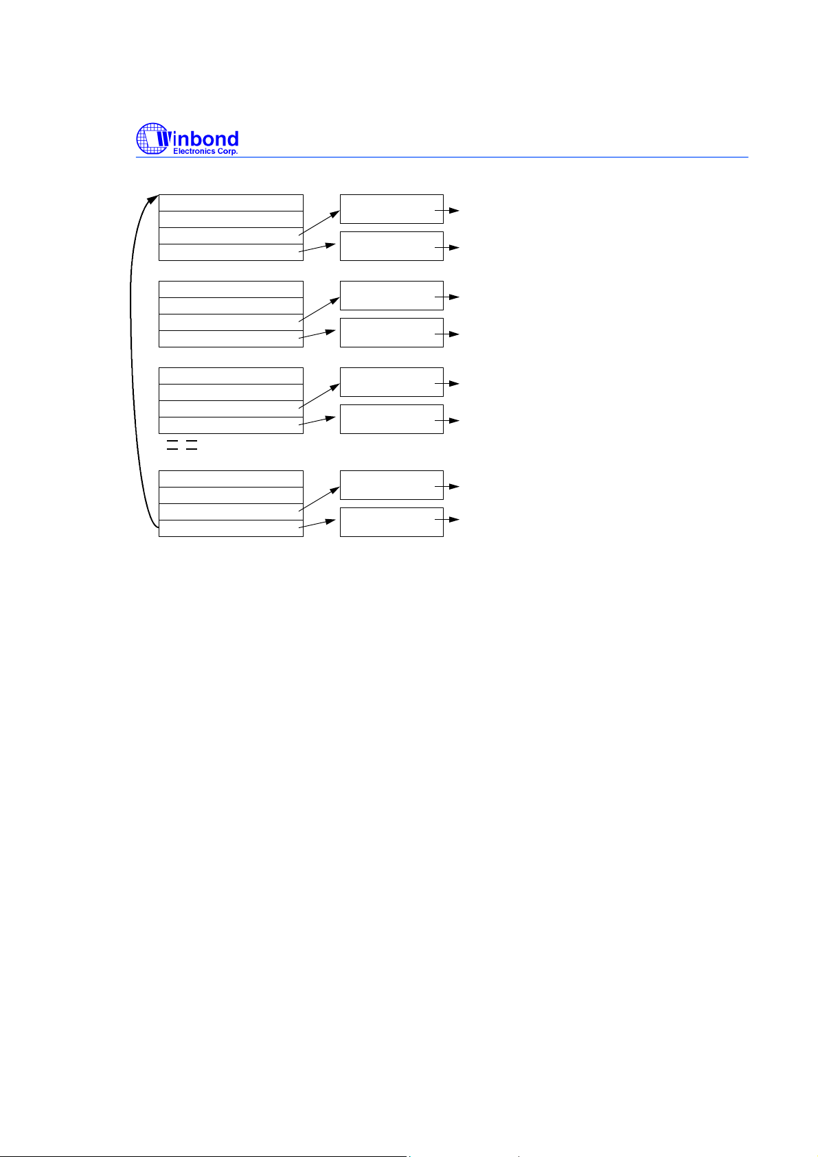
In the descriptors with the ring structure, Host allocates a big continuous memory for keeping all the descriptor
information. Each descriptor can point to two data buffer addresses to store the received packet data. Though the
data buffers are not necessarily be contiguous, the descriptors must be contiguous one after the other.
The following figures describe the ring structures of receive descriptor.
Publication Release Date:October 2000
-14 - Revision 1.01
W89C840AF
first descritpor of Rx descriptor list
status register
structure constructing register
data buffer 1 pointer
data buffer 2 pointer
second descritpor of Rx descriptor list
status register
structure constructing register
data buffer 1 pointer
data buffer 2 pointer
third descritpor of Rx descriptor list
status register
structure constructing register
data buffer 1 pointer
data buffer 2 pointer
last descritpor of Rx descriptor list
status register
structure constructing register
data buffer 1 pointer
data buffer 2 pointer
The software driver can request more than one descriptors and data buffers at a time. As described in the
above diagram, the total descriptors are constructed as a ring. A packet can be stored in more than one data
buffers. In that case, the data buffer 1 is stored first and then data buffer 2. If a packet contains more data than the
two data buffer can accommodate, it fetches the next descriptor and two new data buffers to save the extra more
data. That is a packet can be stored in more than one descriptors. In the contrary, a descriptor is not allowed to
hold more than one packet. If the data buffer 1 can completely store the received packet, the data buffer 2 will be
left empty and the next packet will be firstly stored at the data buffer 1 in the next descriptor. The diagram shown
above is just one case of the buffer application. When the last descriptor is used by a received packet, the next
descriptor should be the first descriptor of the ring. Once the descriptors are processed by the driver, it can be
released to the ring for later use. In the ring structure, the start address of the next descriptor is specified by the
skip length, bit2 to bit6 of C00/CBCR register, and the start address of the first descriptor is specified by the
C0C/CRDLA register.
For the descriptors with the chain structure, host is allowed to allocate scatterly a block of memory with the
size of 4 long words, linked by the pointer which located at the ext descriptor pointer_ field. Each descriptor has
only one link to a data buffer to store the received packet data. The descriptors are located randomly and linked by
the second pointer in each descriptor, which points to the start address of the next descriptor.
The following figures describe the chain structures of receive descriptor.
data buffer 1
data buffer 2
data buffer 1
data buffer 2
data buffer 1
data buffer 2
data buffer 1
data buffer 2
for storing the first RX packet data
for storing the first RX packet data
for storing the 2nd RX packet data
for storing the 2nd RX packet data
for storing the 3rd RX packet data
for storing the 3rd RX packet data
for storing the nth RX packet data
for storing the nth RX packet data
Publication Release Date:October 2000
-15 - Revision 1.01
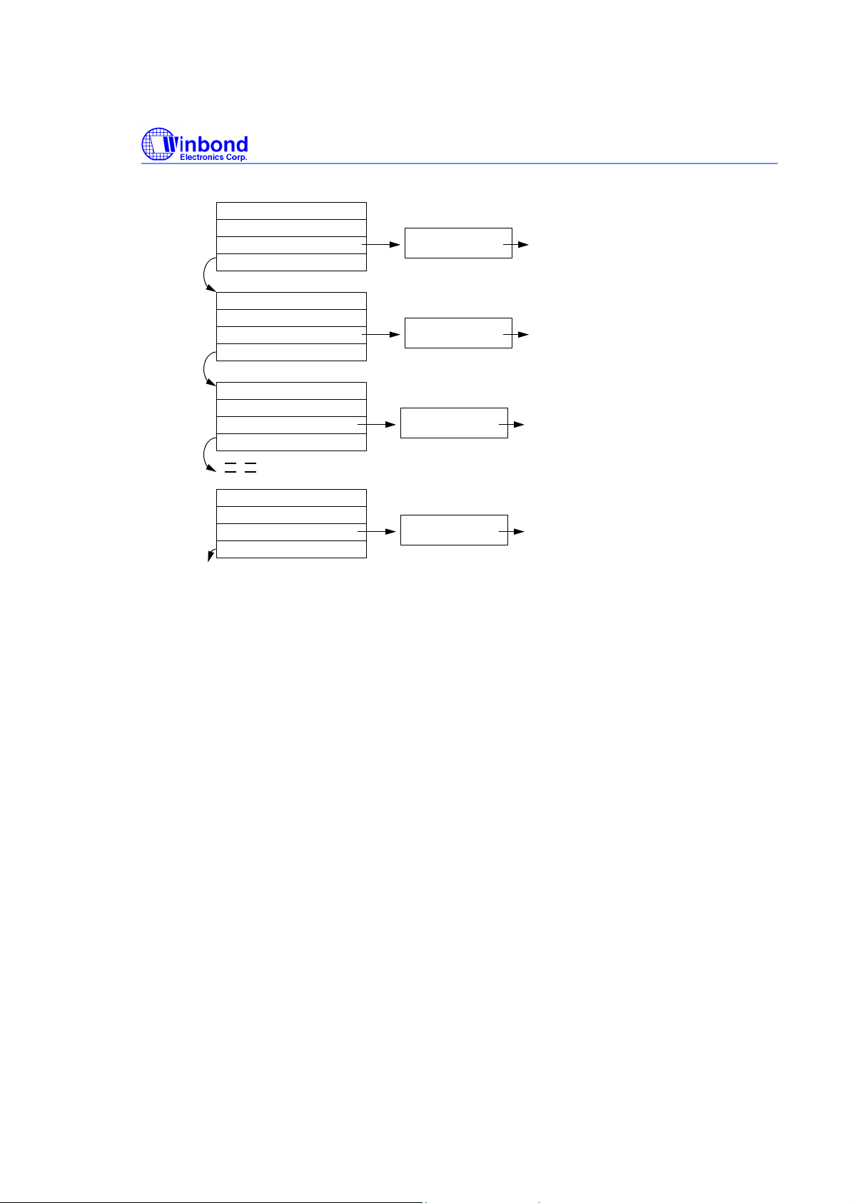
first descritpor of the RX descriptor
status register
structure constructing register
data buffer 1 pointer
next descriptor pointer
second descritpor of the RX descriptor
status register
structure constructing register
data buffer 1 pointer
next descriptor pointer
third descritpor of the RX descriptor
status register
structure constructing register
data buffer 1 pointer
next descriptor pointer
last descritpor of the RX descriptor
status register
structure constructing register
data buffer 1 pointer
next descriptor pointer
W89C840AF
data buffer 1
data buffer 1 for storing the 2nd RX packet data
data buffer 1 for storing the 3rd RX packet data
data buffer 1 for storing the nth RX packet data
for storing the first RX packet data
As shown in the above diagram, descriptors are linked by pointers to construct a chain. The data can be
stored in more than one data buffers. In the last descriptor of the descriptor chain, the content of the R03 register
will be ignored by the receive DMA state machine if the RLINK bit of the R01 register in the last descriptor is set to
high. When the last descriptor has already been used, the next descriptor pointer in this one will link to the start
address of the first descriptor in the chain if it is available.
In the chain structure, the base address of the first descriptors is specified by the C0C/CRDLA register, the
receiving descriptors list address register and the base address of the next descriptor is pointed by the R03 of the
current descriptor.
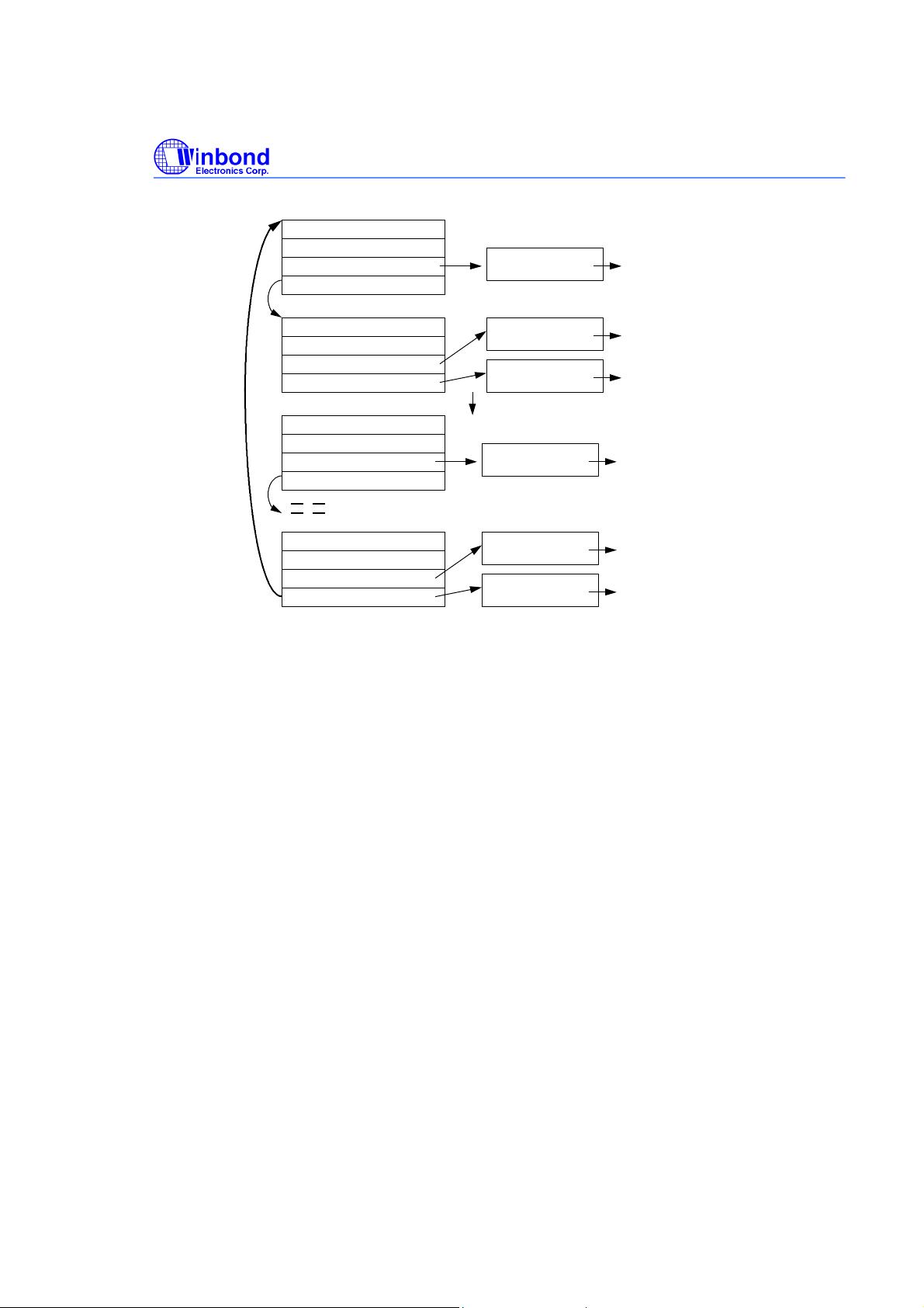
The following figure describes the mixed mode list, composed of both the ring and the chain structures at the
same time.
Publication Release Date:October 2000
-16 - Revision 1.01
W89C840AF
first descritpor of the RX descriptor
status register
structure constructing register
data buffer 1 pointer
next descriptor pointer
second descritpor of the RX descriptor
status register
structure constructing register
data buffer 1 pointer
next descriptor pointer
third descritpor of the RX descriptor
status register
structure constructing register
data buffer 1 pointer
next descriptor pointer
last descritpor of the RX descriptor
status register
structure constructing register
data buffer 1 pointer
data buffer 2 pointer
data buffer 1
data buffer 1
data buffer 2
skip length between descriptors
data buffer 1 for storing the 3rd RX packet data
data buffer 1
data buffer 2
for storing the first RX packet data
for storing the 2nd RX packet data
for storing the 2nd RX packet data
for storing the nth RX packet data
for storing the nth RX packet data
As shown by the above diagram, the descriptors construct a mixed structure. Each descriptor with the chain
structure can link to only one data buffer and the last 32 bits are treated as the next descriptor pointer. When the
RLINK bit of the current descriptor, other than the last descriptor in the descriptor list, is reset to low and this
descriptor is programmed to be a ring structure, the current descriptor can point to two data buffers and the skip
length between descriptor is used to point to the next descriptor starting address.
In the last descriptor in the descriptor list, the R03 register will be used to designate the base address of the
data buffer 2 while the RLINK bit of the last descriptor is reset to low, but will be ignored if the RLINK bit of the
last descriptor is set to high. That is, if the last descriptor is a ring structure, it acts as a ring and vice versa.
The next descriptor field of the last descriptor will be the starting address of the first descriptor, no matter
what the value of the RLINK bit of the last descriptor is low or high.
The data flow of a packet in the receiving path is shown as the following diagram.
Publication Release Date:October 2000
-17 - Revision 1.01
PCI
W89C840AF
data
buffer 1
data
buffer 2
data
buffer 3
data
buffer n
Rx
descriptor 1
Rx
descriptor 2
Rx
descriptor 3
Rx
descriptor n
data
4 Kbytes FIFO
status
PCI
master
status & control
control
receive
DMA
state machine
PCI slave
data
from MAC
controls
from MAC
As shown the above diagram, the receiving DMA state machine controls the data receiving processing and
the receiving status monitoring. On receiving the data packets, the receiving DMA will start to move these data
from FIFO to the data buffer, pointed by descriptors in the host memory if there is an available data buffer and the
byte count of the data received into the FIFO is larger than or equals to 64 bytes. If the received packet length is
less than 64 bytes and runt packet is not accepted, the receiving DMA will discard this invalid packet and give it a
record in the status register. The receiving DMA will start to move the data in FIFO after the full packet is
received if runt packet is accepted. Once a valid packet is received, the receive DMA will advance the descriptor
pointer for the next incoming packet. However, the current data buffer and the descriptor will be re-used if the
current receiving packet is not a valid packet, i.e. the receive state machine will ignore the previously received
packet data in the data buffer. Each received packet will be treated as a valid packet if it meets the requirement in
the bits 3, 4, 5, 6 and 7 of C18/CNCR register. In some case of the data buffer unavailable temporarily, the
incoming packet data from media will be queued in the FIFO temporarily, meanwhile, the receive DMA will enter
suspend state at this time and a buffer unavailable interrupt will be issued. The receive DMA will start moving the
data whenever the data buffer is available and a receiving operation is demanded, On the other hand, the data will
be lost if the FIFO is overflowed. The receiving status, e.g., the receive descriptor access status, the receive
completion status, the received data byte count, the received packet error status, the received packet data type, ...
and so on., will be written back into the descriptor by the receive DMA when the packet is received successfully.
During receiving a packet, the receive DMA will release the access right of the descriptor and the data
buffer to the driver immediately after the free byte space of the data buffers pointed by the current descriptor is
counted down to zero and the receive DMA will fetch the next available descriptor for the current incoming packet.
It is known that the LLC layer data is packed into the first 64 bytes of the packet in most application program. The
driver and the upper layer application program can read the protocol messages carried in the first 64 bytes of the
incoming packet when the receive DMA release the descriptor and the data buffer for the current incoming packet,
although the current incoming packet is not yet received completely. The function of the receive DMA releasing
the descriptor and the data buffer which have been used during receiving a packet allows the software and the
hardware to process the receiving packet concurrently. This parallel processing of software and the hardware can
improve the system receiving performance significantly.
Publication Release Date:October 2000
-18 - Revision 1.01

W89C840AF
When the incoming packet is received completely, the receive DMA will write the same copy of the packet
receiving status to the first descriptor and the last descriptor of the current frame respectively. The receiving status
includes the receive completion status, the received byte count, the receive error type,...etc. All of the status is
specified in the receive descriptor R00. When the software and hardware are concurrently processing , the software
needs not to go back to read the first descriptor of the current incoming packet for knowing the receive completed
status or other receiving status when it is processing the last descriptor and the data buffer of the current incoming
packet. But, if there is only one descriptor needed for the current incoming packet, all of receiving status will be
updated in the unique descriptor.
The W89C840AF transmit DMA function performs the data transfer from the host memory through onchip PCI bus master into the internal 2 Kbytes transmit FIFO. The transmit DMA state machine will request the
MAC to send out the data in the FIFO onto the MII.
The transmit descriptor is used to set the transmit configuration and to point to the transmit data buffer
locations. Each packet to be transmitted can be described by one or more than one descriptor. And each descriptor
consists of four consecutive long word. The first long word(T00) is for the transmit frame status register. The T00
describes the descriptor access right control, the packet transmitting status,...etc. The second long word(T01) is for
the control register used to specify the transmission configuration, including the CRC inhibit control, padding
function control, the descriptor structure control ... etc. The third long word (T02) is for the first data buffer pointer
and the fourth long word is used as the second data buffer pointer in the ring structure.
The transmit descriptor list also can be constructed as a ring structure or a chain structure. The mixed chain
and ring structure is also allowed to be constructed. The scheme for constructing the transmit descriptor list is
same as the one for receiving descriptor list, but, each transmit data buffer size is limited to under 1 Kbytes other
than the 2 Kbytes receiving data buffer. In the consequence of the 1 Kbytes transmit data buffer, each descriptor
can point to a maximum two 1 Kbytes data buffer totally.
The data flow of the packet transmission is shown as the following diagram
Publication Release Date:October 2000
-19 - Revision 1.01
data
buffer 1
data
buffer 2
data
buffer 3
data
buffer n
Tx
descriptor 1
Tx
descriptor 2
Tx
descriptor 3
Tx
descriptor n
PCI
data
long word
aligning buffer
PCI
master
PCI slave
control
transmission
DMA
state machine
2 Kbytes
FIFO
W89C840AF
data
to
MAC
controls
from/to
MAC
The data to be transmitted is stored in the transmit data buffer in the host memory. The transmission DMA
state machine will fetch the data in the host memory into the transmit FIFO. when the transmission DMA is started
up. All of the data fetched from the data buffer will be long word aligned before being queued into the transmission
FIFO. The driver program can inform the transmit DMA the location of the data to be transmitted in the host memory
and then the transmit DMA will fetch the data from that location directly. Because the address of the data may not
long word aligned, so that the transmit DMA need to align the data for passing the data to the MAC in a long word
aligned format. The aligned long word data, and then, is queued into the transmit FIFO. The transmission DMA will
not request the MAC to fetch the data in the FIFO for transmitting until the byte count of the data in the FIFO is
reach the threshold defined by C18/CNCR bit 14~20.
The transmission DMA is implemented a pre-fetch function for speeding the transmit performance. With
this implementation, the transmit DMA will pre-fetch the next packet data in the host memory after the current
packet data is moved into the transmit FIFO completely. Before starting to fetch the next packet data, the transmit
DMA will assert an interrupt if the transmit early interrupt is enabled. If there is no more packet to be transmitted,
the transmit DMA will report a buffer unavailable status and assert an interrupt if the transmit buffer unavailable
interrupt is enabled. After all of the current packet data in the transmit FIFO are transferred out by the MAC block,
the transmit DMA will try to fetch the next packet data again automatically if the transmit DMA is not fetching the
data from the host memory. A packet transmit interrupt will be asserted when the current packet is transmitted if
the packet transmitted interrupt is enabled.
The transmit DMA will write back the current packet transmit status into the first descriptor of the current
transmit packet when the packet is successfully transmitted or is aborted due to excessive collision.
For consecutively transmitting multiple packets, the software driver can previously program all the packet
data in the host memory and then release the access right to the W89C840AF. Once the transmit DMA is turned
on, the DMA will transmit all of the packet out automatically. The inter-frame gap between these packets will be
specified by the MAC block for complying with the IEEE802.3u specification.
Publication Release Date:October 2000
-20 - Revision 1.01

W89C840AF
10101010
1010111
d2
padding
CRC31
0
2
≤
≤
r
For concurrently processing the packets transmitting, the transmission DMA asserts the transmit early
interrupt to trigger the software driver to set up the next transmitting packet data more earlier. The data
transmission rate on the MII bus can be either 10 Mbps or 100 Mbps which is quite lower than the rate on PCI bus.
Mostly, the packet data is not yet completely transmitted onto the MII bus even though the packet data with only a
few bytes have been all moved into the transmit FIFO, the transmission DMA still does not issue an interrupt to
host. This will drop the transmit performance if the software driver waits for the current packet being transmitted
onto the MII completely and then set up the next packet data. The transmit early interrupt can avoid the time
consumption when waiting for the transmit completion of the current packet occurs.
Media Access Control function (MAC)
The function of W89C840AF MAC fully meets the requirements, defined by the IEEE802.3u
specification. The following paragraphs will describe the frame structure and the operation of the transmission
and receive.
The transmission data frame sent from the transmit DMA will be encapsulated by the MAC before
transmitting onto the MII bus. The sent data will be assembled with the preamble, the start frame delimiter
(SFD), the frame check sequence and the padding for enforcing those less than 64 bytes to meet the minimum
size frame and CRC sequence.
The out going frame format will be as following
- - - - 10101010
As mentioned by the above format, the preamble is a consecutive 7-byte long with the pattern
10101010_ and the SFD is a one byte 10101011 data. The padding data will be all 0 value if the sent data frame
is less than 64 bytes. The padding disable function specified in the bit23 of the transmit descriptor T01 is used
to control if the MAC needs to pad data at the end of frame data or not when the transmitted data frame is less
than 64 bytes. The padding data will not be appended if the padding disable bit is set to high. The bits CRC0 ...
CRC31 are the 32 bits cyclic redundancy check(CRC) sequence. The CRC encoding is defined by the following
polynomial specified by the IEEE802.3.
G x x x x x x x x x x x x x x x( ) = + + + + + + + + + + + + +
This 32 bits CRC appending function will be disabled if the Inhibit CRC of the transmission descriptor
T01 is set to high.
The MAC also performs many other transmission functions specified by the IEEE802.3, including the
inter-frame spacing function, collision detection, collision enforcement, collision backoff and retransmission.
The collision backoff timer is a function of the integer slot time, 512 bit times. The number of slot times to
delay between the current transmission attempt to the next attempt is determined by a uniformly distributed
random integer algorithm specified by the IEEE802.3. The integer, r, is specified as the following
32 26 23 22 16 12 11 10 8 7 5 4 2 1
d0 d1
-- dn
CRC30 --- CRC0
k
where k = min(n, 10)
Publication Release Date:October 2000
-21 - Revision 1.01

W89C840AF
The MAC performs the receive functions specified by the IEEE802.3 including the address recognition
function, the frame check sequence validation, the frame disassembly, framing and collision filtering.
The W89C840AF categorizes the input stream from media into three types of frame. These three types
are the packet with uni-cast destination address, the multicast destination address and the broadcast destination
address. A uni-cast address is defined as a destination address with its first bit(the LSB) low. A multicast
address is defined as a destination address with its first bit(the LSB) high but the other 47 bits are not all one. A
broadcast address is defined as a destination address with its all 48 bits are one. All the three types of the packet
reception is selectively determined by the configuration of the bit 3, 4 and 5 of the C18/CNCR register of the
W89C840AF.
The C40/CPA0 and C44/CPA1 are used to store your own 48 bits Ethernet ID. of the network node
before starting to receive a packet. Its contents comes from EEPROM after power-on reset.
The mapping relationship between the 48 bits ID and the C40/CPA0 and C44/CPA1 is as following table.
Bit 31~ 24 Bit 23 ~ 16 Bit 15 ~ 8 Bit 7 ~ 0
C40/CPA0 32th ~ 25th 24th ~ 17th 16th ~ 9th 8th ~ 1st
C44/CPA1 reserved reserved 48th ~ 41th 40th ~ 33th
The incoming packet with unicast address will be accepted if the bit 3 of C18/CNCR is reset to low and
the destination address of the incoming unicast packet has to match with the content of C40/CPA0 and
C44/CPA1 setting.
All of the incoming packet with unicast address will be accepted if the bit 3 of C18/CNCR is set to high.
In broadcast case, to accept a packet with a broadcast destination address, the bit 5 of C18/CNCR must
be set to high. Otherwise, the W89C840AF will reject this broadcast packet.
In multicast case, a packet with a multicast destination address will be accepted if the destination
address is grouped into the selected group specified by the registers of C38/CMA0 and C3C/CMA1. These two
registers are used to store the group mapping for the multicast packet.
The following table shows the group mapping relationship between the groups and the contents of
C38/CMA0 and C3C/CMA1. It is obviously shown that each bit in the registers C38/CMA0 and C3C/CMA1
represents one group.
Bit 31~ 24 Bit 23 ~ 16 Bit 15 ~ 8 Bit 7 ~ 0
C38/CMA0 Group 32 ~ 25 Group 24 ~ 17 Group 16 ~ 9 Group 8 ~ 1
C3C/CMA1 Group 64 ~ 57 Group 56 ~ 49 Group 48 ~ 40 Group 39 ~ 33
Publication Release Date:October 2000
-22 - Revision 1.01

W89C840AF
All the 48 bits destination address(including physical address, multicast address and broadcast address)
of the incoming packet will be fed into the CRC generating mechanism. The six most significant bits of the
CRC(CRC31, CRC30, ... CRC26) will determine which group the incoming packet belongs to. The relationship
between these six bits of CRC content and the group which the multicast address belongs to is shown as the
following table.
CRC CRC28,27,26
31,30,29 111 110 101 100 011 010 001 000
000 grp 8 grp 7 grp 6 grp 5 grp 4 grp 3 grp 2 grp 1
001 grp 16 grp 15 grp 14 grp 13 grp 12 grp 11 grp 10 grp 9
010 grp 24 grp 23 grp 22 grp 21 grp 20 grp 19 grp 18 grp 17
011 grp 32 grp 31 grp 30 grp 29 grp 28 grp 27 grp 26 grp 25
100 grp 40 grp 39 grp 38 grp 37 grp 36 grp 35 grp 34 grp 33
101 grp 48 grp 47 grp 46 grp 45 grp 44 grp 43 grp 42 grp 41
110 grp 56 grp 55 grp 54 grp 53 grp 52 grp 51 grp 50 grp 49
111 grp 64 grp 63 grp 62 grp 61 grp 60 grp 59 grp 58 grp 57
A packet with multicast address which belongs to the nth group will be accepted if the relative bit of the
nth group in C38/CMA0 and C3C/CMA1 is set to high and the bit 4 of C18/CNCR is also set to high.
Besides the address recognition function, the MAC also performs the frame check sequence validation
function. Each incoming packet data, including the destination address, source address, the packet data and the
4 bytes CRC data will be fed into the MAC CRC generating logic to generate a 4 bytes CRC sequence. The
MAC will compare this new CRC data with the one, included in the incoming packet. It will be recognized as
an error packet if these two 4-byte CRC data is not the same. But the bit 7 of C18/CNCR will determine if the
MAC accepts the error packet or not. A high value of this bit will force MAC to accept the error packet, and
low to reject. An incoming packet without byte alignment will be treated as an error packet. Some packets with
the length less than 64 bytes caused by the collision event on the network are also treated as an error packet.
The terminology for the packet with the length less than 64 bytes is called as runt packet. The extra control bit
for accepting the runt packet is defined as the bit 6 of C18/CNCR. To accept a runt packet, both of the bit 6 and
bit 7 of C18/CNCR should be set to high.
The MAC will, finally, do the framing function to strip the preamble and the SFD before sending the
receive data to the receive DMA machine. The data sent to the receive DMA state machine includes the LLC
data and the 4 bytes CRC.
Loopback diagnostics function
The loopback mode defined for W89C840AF is used for diagnostic. The transmit out data will appear
on the MII interface and will then be fed back into the internal receive channel of the MAC block and then be
Publication Release Date:October 2000
-23 - Revision 1.01

W89C840AF
moved back into the host memory by the receive DMA state machine. In loopback mode, the transmission
function will work normally as it is in normal mode, but, only the data is processed by the MAC. The COL,
CRS will be ignored in loopback mode.
To program the W89C840AF into loopback mode, the Loopback Mode of C18/CNCR should be set to
01H.
Full duplex and half duplex function
The transmit DMA and the receive DMA are independently operating no matter what the
W89C840AF is set in full duplex mode or in half duplex mode. However, in MAC side, the operations are
different and depends on the full duplex or half duplex mode is selected.
In the half duplex mode, the MAC should perform the transmission or reception operation at the
different time frame. Simultaneous transmission and reception operation are not allowed. Once the half
duplex mode is selected, the MII input signals, COL and CRS , will be valid inputs for the W89C840AF.
During the time the MAC is transmitting a packet, an active signal COL on MII bus will be judged to be a
transmit collision event, occurred on the media. However, in the time duration from 10 bits time to 16 bits
time after the packet is transmitted, the active COL signal is recognized as a SQE test signal but not a
collision event. The active signal CRS will be recognized as a loopback carrier sense signal when the MAC is
transmitting a packet. The carrier sense lost status is relied on the CRS. Normally, there should not be any
carrier sense lost during transmitting if the media and devices are functional.
In the full duplex mode, the MAC can perform the transmission and receive operation at the same
time. In this case, the COL and CRS signal on MII will be ignored. There are no collision event, SQE lost and
carrier sense lost defined in the full duplex mode. Any activity on COL and CRS will not affect the operation
inside the MAC.
To select the full duplex mode or the half duplex mode, you have to set the full duplex control bit of
C18/CNCR.
Network media speed selection function
The W89C840AF is specifically designed for both 100BASE-T and 10BASE-T Ethernet. The
transmission rate is based on the clock speed of the MII input signals TXCLK and RXCLK. The MAC will
transmit the data based on the clock rate of TXCLK, and receive the MII input data based on the clock rate of
RXCLK.
In 100BASE mode, the TXCLK and RXCLK will be at 25MHz, however, in 10BASE mode, the
TXCLK and RXCLK will be at 2.5 MHz. The clock rate of the RXCLK and the TXCLK is dependent and
determined by the external physical layer device(PHY) which supports 10/100M bit rate.
Publication Release Date:October 2000
-24 - Revision 1.01

W89C840AF
The Fast_Ethernet_Select in C18/CNCR register is used to select the mode in which the W89C840AF
is working in 10M or 100Mbps. In 100Mbps (100BASE) mode, the MAC will not check the SQE status when
transmitting a packet. In 10Mbps(10BASE) mode, the SQE signal will be checked by MAC. No further
function is controlled by the Fast_Ethernet_Select of C18/CNCR register.
Device identifying function
This function is to utilize the device configuration data stored in the device configuration registers, in
which some of them loaded from the external EEPROM. You can tell the vendor, device type, revision,
signature and your own defined code through reading the contents of these registers.
The F00/FID is a read-only register which contains the vendor ID. and device ID., used for
identification. Its_ contents is loaded from the external EEPROM when hardware reset only.
The second read only register F08/FREV used for identification. It contains the revision ID. which is
also loaded from EEPROM only. The Ethernet device identification code is also included in F08/FREV, but it
is a built in code, not loaded form EEPROM.
Another identification register is the F40/FSR, a read only, too. The signature code for Winbond
W89C840AF is built in the F40/FSR signature register. The 12Hth and 9aHth bytes will be read out
recursively when a number of consecutive PCI configuration space read operation is accessed to the F40/FSR.
The first, third, fifth,...etc. odd read operation will get 12H, however, the second, fourth, sixth,...etc. even read
operation will get 9aH.
For some special requirement, the field of driver area of F40/FSR can be used as a word-width data
buffer for latching the user defined identification code.
EEPROM hardware reset auto load and software programming function
The following configuration parameters should be stored in a EEPROM device for configuring the
W89C840AF and can be loaded into the corresponding configuration register while power-on reset occurring.
1) 6 bytes Ethernet ID.
2) 2 bytes subsystem ID.
3) 2 bytes subsystem vendor ID.
4) 2 bytes device ID.
5) 2 bytes vendor ID.
6) 1 bytes revision ID.
7) 1 byte booting device size, power Management capability support and remote wake-up from LAN
8) 1 byte maximum latency
9) 1 byte minimum grant
Publication Release Date:October 2000
-25 - Revision 1.01
 Loading...