

Winbond Electronics W88113CF, W88113CD Datasheet

W88113C
ATAPI CD-ROM
Decoder & Controller

W88113C Data Sheet Revision History
Pages Dates Version Version
on Web
1 N/A 05/1998 0.50 First published
2 16,18,53,54,
56,61,64,67,
70,71,72,73,
p86(add),91,
92,94,95,96
3 1,5,14,21,46,6603/1999 0.61 text error fix
4
5
6
7
8
9
12/1998 0.60 for W88113C version F
Main Contents
10
Please note that all data and specifications are subject to change without notice. All
the trade marks of products and companies mentioned in this data sheet belong to
their respective owners.
LIFE SUPPORT APPLICATIONS
These products are not designed for use in life support appliances, devices, or
systems where malfunction of these products can reasonably be expected to result
in personal injury. Winbond customers using or selling these products for use in
such applications do so at their own risk and agree to fully indemnify Winbond for
any damages resulting from such improper use or sales.

W88113C
TABLE OF CONTENTS
1. OVERVIEW.............................................................................................................1
1.1 FEATURES ........................................................................................................................................... 1
1.1.1 Host Interface ................................................................................................................................... 1
1.1.2 DSP Interface....................................................................................................................................1
1.1.3 Microcontroller Interface ..................................................................................................................1
1.1.4 DRAM Interface...............................................................................................................................2
1.1.5 Audio Playback Interface ..................................................................................................................2
1.1.6 Miscellaneous...................................................................................................................................2
1.2 BLOCK DIAGRAM..............................................................................................................................3
1.3 PIN CONFIGURATION.......................................................................................................................4
1.4 PIN DESCRIPTION..............................................................................................................................5
1.5 PIN TABLE...........................................................................................................................................8
1.6 DEFINITIONS.....................................................................................................................................11
2. REGISTERS DESCRIPTION ................................................................................13
3. REGISTER TABLE...............................................................................................70
4. CHARACTERISTICS ............................................................................................74
5. APPLICATION NOTES.........................................................................................75
5.1 DRAM INTERFACE........................................................................................................................... 75
5.1.1 Memory Layout............................................................................................................................... 75
5.1.2 Block Configuration........................................................................................................................ 76
5.1.3 Linear Address v.s. Block-Offset Address .......................................................................................78
5.1.4 16-bit DRAM..................................................................................................................................79
5.1.5 EDO DRAM................................................................................................................................... 79
Publication Release Date: Mar. 1999
- I - Revision 0.61

W88113C
5.2 MICROCONTROLLER INTERFACE..............................................................................................80
5.2.1 Direct Register Addressing ............................................................................................................. 80
5.2.2 General I/O.....................................................................................................................................81
5.2.3 Programmable System Clock ..........................................................................................................81
5.3 HOST INTERFACE............................................................................................................................83
5.3.1 Ultra DMA Mode Setting................................................................................................................83
5.3.2 Ultra DMA Data-out....................................................................................................................... 83
5.3.3 Ultra DMA Error Handling.............................................................................................................84
5.3.4 Ultra DMA Data-In Transfer Diagram ............................................................................................84
5.3.5 Data-in Transfer Flowchart Example..............................................................................................85
5.3.6 BSY Flag Control ..........................................................................................................................86
5.3.7 Pin HIRQ Control ..........................................................................................................................86
5.4 DECODER LOGIC............................................................................................................................. 87
5.4.1 Sync Detection/Insertion.................................................................................................................87
5.4.2 Descramble..................................................................................................................................... 87
5.4.3 Disk-Monitor Mode ........................................................................................................................87
5.4.4 Parallel ECC Correction ................................................................................................................. 87
5.4.5 EDC Checking................................................................................................................................88
5.4.6 Real Time EDC Checking...............................................................................................................88
5.4.7 Decoding Sequence Model..............................................................................................................88
5.4.8 Disc Format Selection..................................................................................................................... 88
5.4.9 CD-DA data & Q-channel Extraction .............................................................................................89
5.4.10 Target Search................................................................................................................................ 90
5.4.11 Automatic Header Comparison ..................................................................................................... 90
5.4.12 Status Collection........................................................................................................................... 90
5.4.13 Decoder Processing Flow ..............................................................................................................91
5.4.14 Buffer-Independent-Correction .....................................................................................................91
5.4.15 Remove Frequent SRIb & Automatic Cache Management ............................................................92
5.5 AUDIO-PLAYBACK..........................................................................................................................94
5.5.1 Configuration Phase........................................................................................................................ 94
5.5.2 Playback Phase ............................................................................................................................... 94
5.5.3 IEC-958 Digital Audio Output........................................................................................................94
5.5.4 Audio Playback Flowchart Example................................................................................................95
6. ORDERING INSTRUCTION..................................................................................96
7. HOW TO READ THE TOP MARKING..................................................................96
8. PACKAGE DIMENSIONS .....................................................................................97
Publication Release Date: Mar. 1999
- II - Revision 0.61

W88113C
ATAPI CD-ROM DECODER & CONTROLLER
1. OVERVIEW
1.1 Features
1.1.1 Host Interface
• Support ATAPI CD-ROM standard (SFF 8020)
• Ultra DMA/33 support to achieve high throughput and data integrity
• 32-byte Data FIFO to increase data throughput
• Support Block-offset transfer and Linear Address transfer
• Automatic ATAPI sequence handling
• Automatic data transfer trigger and cache management
1.1.2 DSP Interface
• Supports CD-ROM, CD-ROM/XA, CD-I, Video-CD, Photo-CD, and CD-Plus formats
• Supports various types of microprocessors and DSPs
• Supports CD-ROM data descrambling
• Supports both real-time correction and buffer-independent correction
• One byte error correction per P-word and Q-word
• Supports error detection of CD-ROM data
• Automatic repeated error correction
• Real time EDC checking logic
• Q-channel extraction by hardware to support precise CD-DA data reading
• Using pin BCK as subcode reference clock
• Target Search and Status Flag Collection to minimize micro-processor overhead
1.1.3 Microcontroller Interface
• Direct Register Addressing (default) and Indirect Register Addressing support
• Programmable ALE pin
• Support 2 programmable general I/O ports and one programmable general input port
Publication Release Date: Mar. 1999
- 1 - Revision 0.61

W88113C
1.1.4 DRAM Interface
• Various DRAMs support (128K x 8, 256K x 8, 1M x 8, 64K x 16, 128K x 16, 256K x 16)
• Supports ring-control-register to add flexibility of DRAM control
• FPG/EDO DRAM support
• Programmable DRAM timing
• Programmable refresh timing
1.1.5 Audio Playback Interface
• Audio playback in CAV mode
• Programmable audio data output pin
• Programmable audio reference clock
• Flexible left-right mute and volume control
• IEC-958 Digital Audio output
1.1.6 Miscellaneous
• Flexible power management
• Programmable internal system clock (up to 4 times fast of crystal input)
• Clock output with various frequency
• 100-pin QFP/LQFP package
Publication Release Date: Mar. 1999
- 2 - Revision 0.61
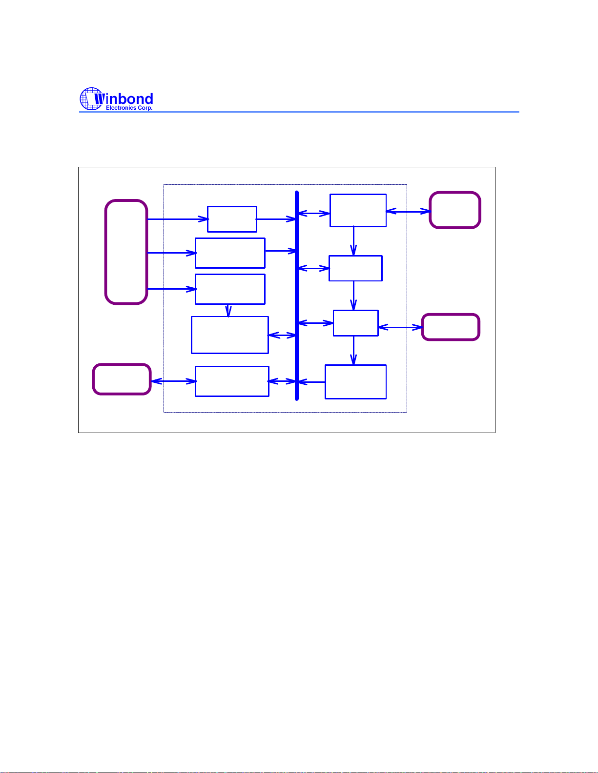
1.2 Block Diagram
Interface
Packet FIFO
DRAM
ATAPI
Interface
Checker
Processor
Checker
W88113C
DSP
Micro-
Subcode
Interface
Sync Detector &
Descrambler
Real Time EDC
Parallel ECC
Corrector & EDC
Microprocessor
Interface
Smart DRAM
Bandwidth
Arbitrator
32 Bytes
Data FIFO
Host
12 Bytes
Command
8/16 bit
FPM/EDO
Publication Release Date: Mar. 1999
- 3 - Revision 0.61
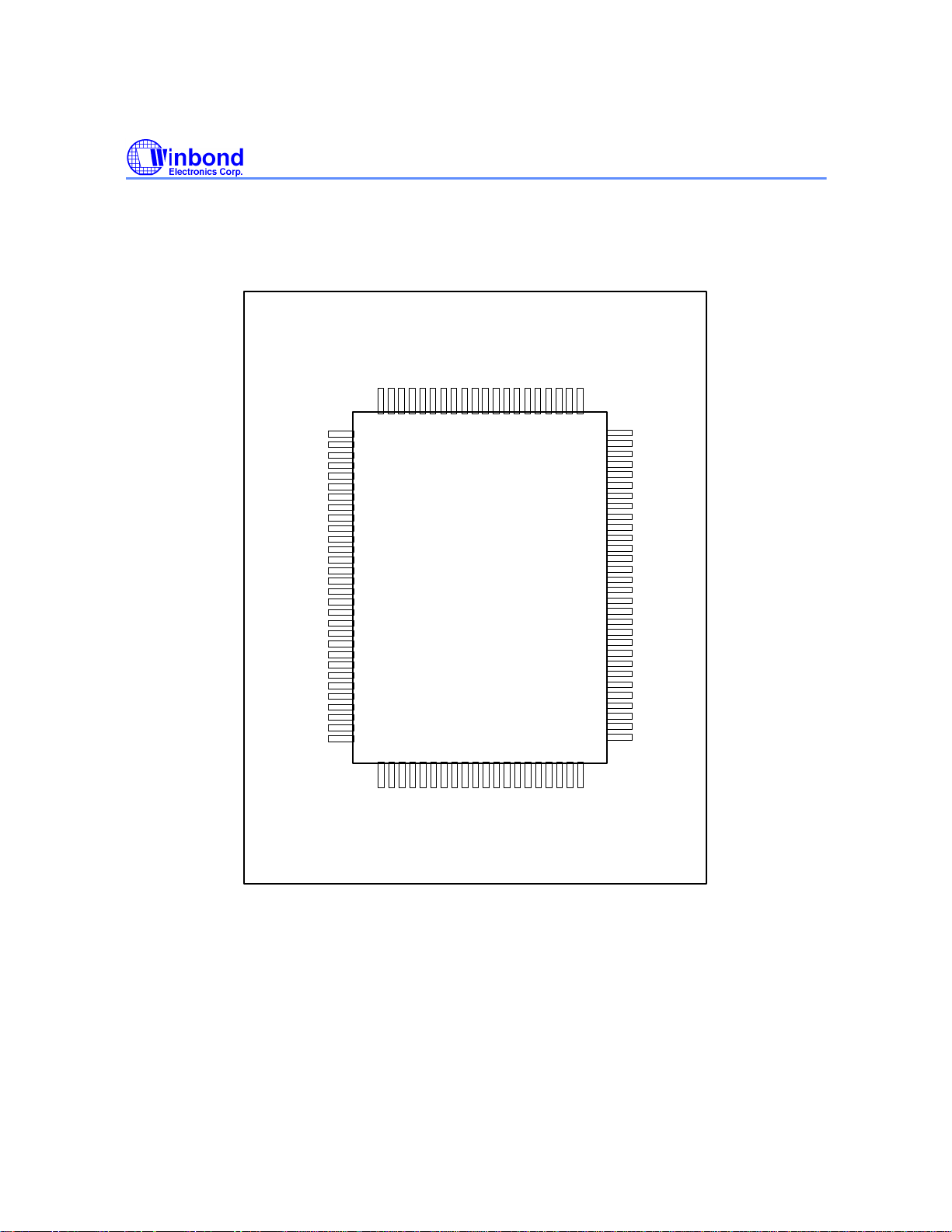
1.3 Pin configuration
W88113C
R
R
O
D
E
8
b
/
/
A
A
R
A
A
A
A
4
0
1
2
R
V
W
D
D
A
A
A
A
A
D
E
1
9
6
5
D
S7
b
8
0
R
R
R
R
R
R
R
R
R
R
C
S
S
R
D
D
1
2
R
R
A
R
R
D
D
D
S
D
D
1
3
2
L
0
3
GND
RA3
CASH
RD11
RD12/ALE1
ABCK
RD14
LRCK
SDATA
BCK
C2PO
RD15/DJ
CLKO/ALRCK
XOUT
XIN
GND
SCSB
WFCK
SCSYN
EXCK
HRSTb/GIO1
UD0
UD1
RD13
UD2
UD3
UD4
UD5
UD6
GND
0
1
0
2
3
4
5
6
7
8
9
10
11
12
13
14
15
16
17
18
19
20
21
22
23
24
25
26
27
28
29
30
313233343536373839404142434445464748495
U
U
D
R
7
S
/
D
A
0
W88113C
U
U
U
U
D
R
W
C
I
A
S
D
R
S
N
P
T
b
b
b
b
b
C
P
D
V
D
C
C
S
S
3
1
b
b
D
S
D
A
D
A
A
1
I
2
D
0
1
6
A
G
b
b
818283848586878889909192939495969798991
0
A
H
I
D
H
I
O
M
R
C
R
R
A
D
L
Q
D
C
b
Y
K
K
b
GND
80
RD6
79
RD7
78
RD5
77
RD4
76
CRSTb
75
DD7
74
DD8
73
SDATA1
72
DD6
71
DD9
70
DD5
69
DD10
68
DD4
67
GND
66
DD11
65
ALE2
64
DD3
63
DD12
62
DD2
61
ARSTb/GIO2
60
DD13
59
ASD0
58
DD1
57
DD14
56
DD0
55
DD15
54
DMARQ
53
HWRb
52
GND
51
Publication Release Date: Mar. 1999
- 4 - Revision 0.61
1.4 Pin Description
The following convention is used in the pin description table below:
(I) denotes an input
(O) denotes an output
(OZ) denotes a tri-state output
(OD) denotes an open-drain output
(I/O) denotes a bi-directional signal
Miscellaneous Pins
NAME NO. TYPE PIN DESCRIPTION
RD15/DJ
CLKO/ALRCK
XIN
XOUT
HRSTb/GIO1
ARSTb/GIO2
CRSTb
VDD
GND
12
13
15
14
17
60
75
41, 89
1, 16, 30, 51,
66, 80
I/O RAM Data 15/Drive Jumper
O Clock Output/Audio LR Clock
I
O
Crystal input/output - Normally, XIN and XOUT are
connected to a crystal.
I Host Reset - A low active input signal
OD ATAPI Reset - A low active output signal.
I Chip Reset - A low-active input signal.
Power Supply Pin - 5.0V ± 5%
Ground Pin
W88113C
Micro-controller Interface
NAME NO. TYPE PIN DESCRIPTION
UD[7:0]
URS/GIN3/D
AO
URDb
UWRb
UCSb
RD12/ALE1
ALE2
UINTb
22, 23, 25, 26,
27, 28, 29, 31
32
33
34
35
5
64
36
I/OZ Microprocessor Data Bus - Bi-directional processor data lines.
I Register Select - To select address register or internal
register.
I Microprocessor Read Strobe - A low-active input signal.
I Microprocessor Write Strobe - A low-active input signal.
I Microprocessor Chip Select - A low-active input signal.
I RAM data 12/Address Latch Enable 1
I Address Latch Enable 2
OD Microprocessor Interrupt - A low-active output signal that can
be externally wired-OR with other interrupt sources.
Publication Release Date: Mar. 1999
- 5 - Revision 0.61
Audio Interface
NAME NO. TYPE PIN DESCRIPTION
ABCK
CLKO/ALRCK
ACLK
ASD0
ROEB/ASD1
RD8/ASD2
Host Interface
6
13
46
58
84
86
W88113C
O Audio Bit Clock
O Audio Left/Right Clock
I Audio Reference Clock
O Audio Serial Data 0
O Audio Serial Data 1
O Audio Serial Data 2
NAME
DD[15:0]
DA[2:0]
DASPb
CS3b
CS1b
PDIAGb
CS16b
HIRQ
DMACKb
IORDY
HRDb
HWRb
DMARQ
NO.
54, 56, 59, 62,
65, 68, 70, 73,
74, 71, 69, 67,
63, 61, 57, 55
40, 44, 42
37
38
39
43
45
47
48
49
50
52
53
TYPE PIN DESCRIPTION
I/OZ Host Data Bus - Signals enable data transfer between the host
and W88113A.
I Host Address Bus - Signals to access various ATAPI registers.
I/OD Drive Active/Drive 1 Present - A time-multiplexed signal
indicating whether a drive is active, or Drive 1 is present.
I Host Chip Select 1 - A low-active input signal used to select the
host Control Block Registers.
I Host Chip Select 0 - A low-active input signal used to select the
host Command Block Registers.
I/OD Passed Diagnostics - A signal asserted by Drive 1 to indicate to
Drive 0 that diagnostic is completed.
OD 16-bit I/O Select - A low-active output signal to indicate a 16-bit
data transfer.
OZ Host Interrupt - A signal to request an interrupt service from
host.
I DMA Acknowledge - A low-active input signal used for DMA
transfer by the host when DMARQ is ready.
OZ I/O Channel Ready - When device is not ready for a data
transfer request, this signal is negated for extension of the host
data transfer cycle within any host register access.
I Host I/O Read - A low-active read strobe signal.
I Host I/O Write - A low-active write strobe signal.
OZ DMA Request - A high-active signal asserted for DMA data
transfer when device is ready to transfer data to or from the
host.
Publication Release Date: Mar. 1999
- 6 - Revision 0.61
W88113C
DSP Interface
NAME NO. TYPE PIN DESCRIPTION
LRCK 8 I L/R Channel Clock - Left and right channels are distinguished by this
signal.
SDATA 9 I Serial Data - Serial data from DSP is received from this input.
SDATA1 72 I Serial Data - Second Serial data from DSP is received from this
input.
BCK 10 I Bit Clock - Bit clock from DSP is received from this input.
C2PO 11 I C2 Pointer - C2 error flag from DSP is received from this input.
Subcode Interface
NAME NO. TYPE PIN DESCRIPTION
SCSD 17 I Subcode Serial Data - Subcode serial data from DSP is received from
this input.
WFCK 18 I Write Frame Clock - Write frame clock from DSP is received from
this input.
SCSYN 19 I Subcode Sync - Subcode sync from DSP is received from this input.
EXCK 20 I/O External Clock - A pin programmed as input or output to supply bit
clock for subcode.
External RAM Interface
NAME NO. TYPE PIN DESCRIPTION
ROEb
RWEb
RD[15:0]
RA[9:0]
CASH/L
RAS
84
88
12, 7, 24, 5, 4,
91, 94, 86, 78,
79, 77, 76, 81,
82, 87, 85
91, 92, 93, 95,
96, 97, 2, 100,
99, 98
3, 83
90
O External RAM Output Enable - A low-active output signal
O External RAM Write Enable - A low-active output signal
I/O RAM Data Bus - Data bus for external RAM.
O RAM Address Bus - Address bus for external RAM.
O External RAM Column Address Strobe
O External RAM Row Address Strobe
Publication Release Date: Mar. 1999
- 7 - Revision 0.61
1.5 Pin Table
W88113C
NO.
1 GND P Ground
2 RA3 O RAM Address 6mA
3 CASH O High Byte Column Address Strobe 6mA
4 RD11 I/O RAM Data 6mA, PU
5 RD12/ALE1 I/O RAM Data/Address Latch Enable 6mA, PU
6 ABCK O Audio Bit Clock 6mA, PU
7 RD14 I/O RAM Data 6mA, PU
8 LRCK I L/R Channel Clock 6mA, PU
9 SDATA I DSP Serial Data
10 BCK I DSP Bit Clock
11 C2PO I DSP C2 Pointer
12 RD15/DJ I/O RAM Data/Drive Jumper 6mA, PU
13 CLKO/ALRCK O Clock Output/Audio LR Clock 6mA, PU
14 XOUT O Crystal Output
15 XIN I Crystal Input
16 GND P Ground
NAME TYPE DESCRIPTION REMARK
17 SCSB I Subcode Serial Data
18 WFCK I Write Frame Clock
19 SCSYN I Subcode Sync
20 EXCK I/O Subcode External Clock 6mA, PU
21 HRSTb I/OD Host Reset/GIO1 6mA, PU
22 UD0 I/O uP Data 6mA, PU
23 UD1 I/O uP Data 6mA, PU
24 RD13 I/O RAM Data 6mA, PU
25 UD2 I/O uP Data 6mA, PU
26 UD3 I/O uP Data 6mA, PU
27 UD4 I/O uP Data 6mA, PU
28 UD5 I/O uP Data 6mA, PU
29 UD6 I/O uP Data 6mA, PU
30 GND P Ground
Publication Release Date: Mar. 1999
- 8 - Revision 0.61
W88113C
1.5 Pin Table, continued
NO.
31 UD7 I/O uP Data 6mA, PU
NAME TYPE DESCRIPTION REMARK
32 URS/DAO/GIN3 I/O uP Register Select/Digital Audio Output 0
General Input 3
33 URDb I uP Read Strobe
34 UWRb I uP Write Strobe
35 UCSb I uP Chip Select
36 UINTb OD uP Interrupt 12mA
37 DASPb I/OD Drive Active 12mA, PU
38 CS3b I Host Chip Select 1 PU
39 CS1b I Host Chip Select 0 PU
40 DA2 I Host Address PU
41 VDD P Power Supply
42 DA0 I Host Address PU
43 PDIAGb I/OD Passed Diagnostics 12mA, PU
44 DA1 I Host Address PU
45 CS16b OD 16-bit I/O Select 12mA
46 ACLK I Audio Reference Clock
47 HIRQ O Host Interrupt 12mA
48 DMACKb I DMA Acknowledge PU
6mA
49 IORDY O I/O Channel Ready 12mA
50 HRDb I Host Read Strobe PU
51 GND P Ground
52 HWRb I Host Write Strobe PU
53 DMARQ O DMA Request 12mA
54 DD15 I/O Host Data 12mA, PU
55 DD0 I/O Host Data 12mA, PU
56 DD14 I/O Host Data 12mA, PU
57 DD1 I/O Host Data 12mA, PU
58 ASD0 O Audio Serial Data 0 6mA
59 DD13 I/O Host Data 12mA, PU
60 ARSTb I/OD ATAPI Reset/GIO2 6mA, PU
Publication Release Date: Mar. 1999
- 9 - Revision 0.61
W88113C
1.5 Pin Table, continued
NO.
61 DD2 I/O Host Data 12mA, PU
62 DD12 I/O Host Data 12mA, PU
63 DD3 I/O Host Data 12mA, PU
64 ALE2 I Address Latch Enable
65 DD11 I/O Host Data 12mA, PU
66 GND P Ground
67 DD4 I/O Host Data 12mA, PU
68 DD10 I/O Host Data 12mA, PU
69 DD5 I/O Host Data 12mA, PU
70 DD9 I/O Host Data 12mA, PU
71 DD6 I/O Host Data 12mA, PU
72 SDATA1 I DSP Serial Data 1
73 DD8 I/O Host Data 12mA, PU
NAME TYPE DESCRIPTION REMARK
74 DD7 I/O Host Data 12mA, PU
75 CRSTb I Chip Reset PU
76 RD4 I/O RAM Data 6mA, PU
77 RD5 I/O RAM Data 6mA, PU
78 RD7 I/O RAM Data 6mA, PU
79 RD6 I/O RAM Data 6mA, PU
80 GND P Ground
81 RD3 I/O RAM Data 6mA, PU
82 RD2 I/O RAM Data 6mA, PU
83 CASL O Low Byte Column Address Strobe 6mA
84 ROEB/ASD1 O RAM Read Strobe/Audio Serial Data 1 6mA, PU
85 RD0 I/O RAM Data 6mA, PU
86 RD8/ASD2 I/O RAM Data/Audio Serial Data 2 6mA, PU
87 RD1 I/O RAM Data 6mA, PU
88 RWEb O RAM Write Strobe 6mA
89 VDD P Power Supply
90 RAS O Row Address Strobe 6mA
Publication Release Date: Mar. 1999
- 10 - Revision 0.61
W88113C
1.5 Pin Table, continued
NO.
91 RD10/RA9 I/O RAM Data/RAM Address 6mA, PU
92 RA8 O RAM Address 6mA, PU
93 RA7 O RAM Address 6mA, PU
94 RD9 I/O RAM Data 6mA, PU
95 RA6 O RAM Address 6mA
96 RA5 O RAM Address 6mA
97 RA4 O RAM Address 6mA
98 RA0 O RAM Address 6mA
99 RA1 O RAM Address 6mA
100 RA2 O RAM Address 6mA
1.6 Definitions
NAME TYPE DESCRIPTION REMARK
Asserted/Activated:
Asserted and activated mean that a signal is driven to its true state.
Block:
This term refers to the data in one logical block. The block size depends on the parameter of packet
command.
Block-Offset/Linear Address:
The block-offset address is an indirect mapping to the external RAM. The offset range is limited by
the block size. The linear address is a direct mapping to the external RAM.
Command Packet (CP):
The command packet is the structure used to communicate commands from a host computer to an
ATAPI device. All CD-ROM command packets are 12 bytes in length.
Data-in/Data-out Transfer:
During the data-in transfer, the data is transferred from device to host. During the data-out transfer,
the data is transferred from host to drive.
Publication Release Date: Mar. 1999
- 11 - Revision 0.61

W88113C
Decrement/Increment:
Decrement means that a value minus 1. Increment means that a value plus 1.
Negated/De-activated:
Negated and de-activated mean that a signal is driven to its false state.
Sector:
This term refers to the data contained by one frame time (1/75s for 1x).
Ultra DMA:
Ultra DMA is a data transfer protocol that applies to the Ultra DMA data burst only.
Ultra DMA burst:
An Ultra DMA burst is defined as the period from an assertion of DMACKb to the subsequent
negation of DMACKb when Ultra DMA has been enabled by the host.
Ultra DMA CRC:
Cyclical Redundancy Check is used for the Ultra DMA protocol to check the validity of the data that
has been transferred during last Ultra DMA burst.
Publication Release Date: Mar. 1999
- 12 - Revision 0.61

W88113C
2. REGISTERS DESCRIPTION
IR - Index Register (read/write)
If DRA (5Bh.1) is high, the Index Register is latched at the falling edge of pin ALE1 (5) or pin ALE2
(64) depending on the setting of ALE2 (5Ch.3).
If DRA (5Bh.1) is low and pin URS (32) is low, the Index Register can be accessed by the
microprocessor. The value in IR specifies which internal register to be accessed by microprocessor
when pin URS (32) is high.
Note that the 4 least significant bits of IR will increment following each read or write to any register except for PFAR (00h,r). Since IR
does not automatically increment from 00h to 01h, consecutive reads to address 00h will repeatedly read register PFAR (00h,r). This
feature accelerates read operation of ATAPI Command Packet.
PFAR - Packet FIFO Access Register - (read 00h)
While SCoD (20h.2) is high, the ATAPI Command Packet issued from host is received by the 12-byte
Packet FIFO. Flag TENDb (01h.r6) is used to check if the Packet FIFO is full. The microprocessor
can read the ATAPI Command Packet by repeatedly read register PFAR (00h,r). Once the FIFO
becomes empty, the value FFh will be returned if microprocessor read PFAR.
The Packet FIFO can also be used to receive command parameter less than 12 bytes. First, the
control bit SCoD (20h.2) is set high to select the Packet FIFO to be addressed by the ATAPI Data
port. When DRQ (37h.3) changes from 0 to 1, the lower 4 bits of ATBLO (34h) is latched as the FIFO
threshold. Upon the number of bytes in the FIFO reaches the threshold, flag TENDb (01h.r6)
becomes active-low and flag FPKT (30h.r1) becomes active-high. Once FPKT becomes high, any
data writes to the ATAPI Data port is rejected.
INTCTL - Interrupt Control Register - (write 01h)
Bit 7: PFNEEN - Packet FIFO Not Empty Interrupt Enable
Pin UINTb (36) is activated when PFNEb(01h.r7) becomes active-low if this bit is high.
Bit 6: TENDEN - Transfer End Interrupt Enable
Pin UINTb (36) is activated when TENDb (01h.r6) becomes active-low if this bit is high. This
bit is also automatically enabled if the host issues the Packet Command (A0h) while HIIEN
(2Eh.w7) is high and drive is selected.
Bit 5: SRIEN - Sector Ready Interrupt Enable
Pin UINTb (36) is activated when SRIb (01h.r5) becomes active-low if this bit is high. This bit
is clear to 0 after chip reset, host reset, firmware reset and decoder reset.
- 13 - Revision 0.61
Publication Release Date: Mar. 1999
Bits 4, 3, 2: Reserved
Bit 1: DTEN - Data Transfer Enable
Set this bit high enables the data transfer logic. This bit should be set before trigger any data
transfer. In order to reduce the interference of microprocessor, this bit is also automatically
enabled during the following operation:
• Trigger ADTT (17h.w2)
• Host issues ATAPI Packet Command (A0h) while APKTEN (18h.7) is enabled and drive is
selected
In case of un-recoverable transfer error, setting this bit low will terminate the current data
transfer immediately.
Bit 0: Reserved
INTREA - Interrupt Reason Register - (read 01h)
Bit 7: PFNEb - Packet FIFO Not Empty Interrupt Flag
This bit becomes active-low after Packet FIFOs receive any data issued by the host through
ATAPI Data port. Pin UINTb (36) is activated when this bit becomes active-low if PFNEEN
(01h.w7) is enabled. This flag is deactivated after the last byte is read by microprocessor
through register PFAR (00h,r).
Bit 6: TENDb - Transfer End Interrupt Flag
This bit becomes active-low at the end of data transfers. Flag TDIR (30h.r5) and FPKT
(30h.r1) can be used to determine which type of transfer end occurs. Pin UINTb (36) is
activated when this bit becomes active-low if TENDEN (01h.w6) is enabled.
W88113C
TENDb
(01h.r6)
0 1 0 data-in transfer DHTACK (0Eh), TACK (07h)
0 1 x data-out transfer TACK (07h)
0 0 x A0 command packet transfer TACK (07h)
Bit 5: SRIb - Sector Ready Interrupt Flag
If RMSRI (5Ch.0) is low, this bit is used to indicate that one sector is ready to be accessed. If
RMSRI (5Ch.0) is high, this bit is generated only by STAERR (80h.r6), BIN0 (80h.r5), DSFULI
(80h.r4), LASTBK (80h.r3), LTTI (80h.r2), TNFI (80h.r1) or HCEI (80h.r0).
Reading register STAT3 (0Fh,r), LSTA3 (4Bh,r) or TARSTA (80h,r) deactivates this flag.
TDIR
(30h.r5)
FPKT
(30h.1)
Transfer End Reason Acknowledge register
Publication Release Date: Mar. 1999
- 14 - Revision 0.61

Bit 4: HCIb - Host Command Interrupt Flag
This bit is activated by the following events:
• Host issues ATAPI Soft Reset Command, if ARSTIEN(2Fh.1) is enabled
• Host issues command to a non-exist slave drive, if SHIEN(2Eh.2) is enabled
• Host issues Execute Drive Diagnostics Command, if HIIEN(2Eh.7) is enabled
• ATAC(2Fh.6) becomes active-high, if HIIEN(2Eh.7) is enabled
• Host set bit SRST in ATAPI Device Control Register, if HIIEN(2Eh.7) is enabled
Bit 3: TBSYb - Transfer Busy Flag
This bit becomes active-low when the data transfer to host is triggered by the following
events:
• Writing any value to register THTRG (06h,w)
• Setting bit ADTT (17h.w2) high
After host read the last byte to be transferred, this flag is deactivated.
Bit 2: APIb - Audio Playback Interrupt Flag
If APOUT (90h,1-0) are not zero, this bit is used as audio-playback-interrupt flag.
Bit 1: DFRDYb - Data FIFO Ready
After data transfer is triggered, the 32-byte Data FIFOs is automatically filled. This bit is used
to indicate that the Data FIFOs is ready to be read by the host for debugging. The Data FIFO
is automatically cleared in any of the following conditions:
• Chip reset, host reset and firmware reset
• DTEN (01h.w1) is 0
• DINB (1Fh.w1) is 1
• DFRST (2Bh.w3) is 1
• The end of data-in transfer
Bit 0: SCIb - Subcode Interrupt Flag
If SCIEN (2Ch.w4) is enabled, this bit becomes active-low when one of the following events
occurs:
W88113C
• ISS (22h.r0) becomes active-high
• NESBK (22h.r1) becomes active-high
• MSS (22h.r2) becomes active-high
When Subcode Interrupt is activated, the microprocessor can read register SUBSTA (22h,r)
to determine the reason of interrupt. Writing register SCIACK (22h,w) deactivates this flag
Publication Release Date: Mar. 1999
- 15 - Revision 0.61

W88113C
TWCL - Transfer Word Counter Low- (read/write 02h)
Before triggering data transfer, the number of words to be transferred should be set through 12-bit
Transfer Word Counter (TWC). The number of words minus 1 should be written to this counter while
using standard ATAPI 16-bit data transfer. After host read one word, the counter is decreased by
one. Transfer End Interrupt Flag, TENDb (01h.r6), is activated when this counter becomes zero.
Bit 7-0: TWCH[7:0] - Transfer Word Count Low
TWCH - Transfer Word Counter High - (read/write 03h)
Bit 7: LATXF - Linear Address Transfer Enable
If this bit is high, the Linear Address Transfer is enabled. In this case, the data stored from
the address specified by RAC (2Dh,1Dh,1Ch) are transferred to host after trigger. The size of
transfer data is limited by TWC (03h/02h). Setting this bit high cause UTBY (1Fh.r7) high to
inhibit uP to access RAMRD (1Eh,r) or RAMWR (1Eh,w).
If this bit is low, the Block-Offset Transfer is enabled. In this case, the data stored from the
address specified by TBH/L (25h/24h) and TACH/L (05h/04h) are transferred to host after
trigger. The address of data warps around at the block boundary, so the size of transfer data
is limited by block size.
Bit 3-0: TWCH[3:0] - Transfer Word Count High
TACL/TACH - Transfer Address Counter - (write 04h/05h)
Before triggering block-offset data transfer, the external RAM address of data to be transferred should
be set through TACH/L (05h/04h,w). This number in this counter specifies the first available data
address relative to the beginning of the block. The block number should also be specified through
Transfer Block registers TBH/L (25h/24h). After one word is read by host, TACH/L are incremented to
the next available data address. The following equation illustrates the relation between block-offset
and linear address:
linear address = (block number × block size) + address offset
THTRG - Transfer to Host Trigger Register - (write 06h)
This register is used to trigger data transfer regardless of what value is written. If DINB (1Fh.1) is low,
triggering this register automatically fills the Data FIFO and then flag DFRDYb (01h.r1) becomes
active-low when the Data FIFO becomes ready. If DINB (1Fh.1) is high, data-out transfer is enabled,
e.g., parameter of mode-select command. A more convenient way is set ADTT (17h.w2) high and
then trigger hardware data transfer sequence.
Publication Release Date: Mar. 1999
- 16 - Revision 0.61
W88113C
TACK - Transfer Acknowledge - (write 07h)
Writing this register deactivates flag TENDb (01h.r6) and its corresponding interrupt regardless of
what data is written.
HEAD0 to HEAD3 - Header Registers - (read 03h to 07h)
These four registers are used to hold the information of Header Bytes of each sector. Header
Registers should be read soon after STAVAb (0Fh.r7) becomes active-low. Note that the header
bytes are distrustful if wrong mode is set while ECC is enabled. If bit SHDEN (0Bh.w0) is enabled,
registers HEAD0-3 are used to hold subheader bytes instead.
If control bit QMSF (80h.w4) is set high, the corresponding MSF bytes in Q-channel information
would be automatically loaded into HEAD0-2 (04h-06h,r) when each byte is ready from DSP. Notice
that the value in register HEAD3 (07h,r) and SUBH0-3 (14h-17h,r) are not available in this case.
BIAL/BIAH - Buffering Initial Address - (write 08h/09h)
The rule for configuration is that the first byte of the sector is stored at
BIAH/L(09h/08h) - 0Ch
Before enabling the external RAM buffering through CTRL0 (0Ah,w), BIAH/L should be set to control
the location of the first byte follows data sync for each data sector. The RAM block for buffering is
controlled by the number in registers DDBH/L(29h/28h) plus one. For convenience of following data
transfer, the microprocessor may set proper value to BIAH/L after the mode is determined so that the
first user data byte will locate at offset 00h of each data block.
BIAH/L(08h/09h)
first sync
first header
first subheader
first data
CD-DA yellow book
mode 1 & mode 2
000Ch FFFCh FFF4h
n/a FFF0h FFE8h
n/a FFFCh FFF4h
n/a n/a FFF8h
0000h 0000h 0000h
CD-ROM XA
mode 2
BACL, BACH - Buffering Address Counter - (read 0Ah/0Bh)
After enabling the external RAM buffering, Buffering Write Counter is automatically increased by two,
beginning from the value specified by BIAH/L (09h/08h,w), every time a data word is buffered.
Publication Release Date: Mar. 1999
- 17 - Revision 0.61

W88113C
EIAL/EIAH - ECC Initial Address - (read 08h/09h, write 0Ch/0Dh)
EIAH/L are used to hold the initial address offset of the data block to be corrected. The content of
BIAH/L (09h/08h,w) will be automatically loaded to EIAH/L at the beginning of each data sync,
making it unnecessary to read or write EIAH/L during normal operation. The RAM block for ECC is
controlled by the number in registers DDBH/L (29h/28h).
CTRL0 - Control Register 0 - (write 0Ah)
This register is 0 after chip reset, host reset, firmware reset and decoder reset.
Bit 7: DECEN - Decoding Logic Enable
Setting this bit high enables the decoding logic.
Bit 6: RTEDC - Real Time EDC Checking Enable
Setting this bit high enables the real-time-EDC-checking logic. The RSPC error correction is
performed only when the result of real time EDC check is error. This function could save
about 2/3 of DRAM bandwidth compared with conventional decoder.
Bit 5: EDCEN - Error Detect and Correct Enable
Setting this bit high enables the ECC and EDC logic. Change of this bit takes effect after next
sync.
Bit 4: ACEN - Automatic Correction Enable
If both M2RQ (0Bh.w3) and this bit is high, the type of error correction is automatically
determined by FORM bit in the subheader byte. If only M2RQ (0Bh.w3) is high, the type of
error correction is controlled by F2RQ (0Bh.w2). If M2RQ (0Bh.w3) is low, this bit does not
affect the correction of mode 1 data.
Bit 3: PKTINH - obsolete
Bit 2: BUFEN - Buffering Enable
Setting this bit high enables incoming DSP data buffering. When this bit is high, the values
of register HEAD0-3(04h-07h) and SUBH0-3(14h-17h) are retrieved from external RAM rather
than from incoming serial data. When BUFEN is low, any setting of QCEN or PCEN is
meaningless. Change of this bit takes effect after next sync.
Bit 1: QCEN - Q-codeword Correction Enable
When this bit is high, Q-codeword RSPC correction logic is enabled. Change of this bit takes
effect after next sync.
Bit 0: PCEN - P-codeword Correction Enable
When this bit is high, P-codeword RSPC correction logic is enabled. Change of this bit takes
effect after next sync.
Publication Release Date: Mar. 1999
- 18 - Revision 0.61
W88113C
DECEN
0Ah.7
1 1 1 1 1 Q-P correction
1 1 1 1 0 Q-correction
1 1 1 0 1 P-correction
1 1 1 0 0 Buffer-only CRC
1 0 0 0 0 Disk-monitor no buffering
0 X X X X Decoder
Note that if ATMSEN (9Ah.6) is high, the decoder logic will operate in Disk-monitor mode before the
target is found. When the target is found, the setting of register CTRL1 (0Bh,w) will be automatically
loaded into decoder logic.
BUFEN
0Ah.2
EDCEN
0Ah.5
QCEN
0Ah.1
PCEN
0Ah.0
Decoder
Mode
disable
Operation
Flow
Q → P → CRC
Q → CRC
P → CRC
no operation
CTRL1 - Control Register 1 - (write 0Bh)
This register is 0 after chip reset, host reset, firmware reset and decoder reset.
Bit 7: SIEN - Sync Insertion Enable
When this bit is high, the sector boundary is determined by internal sync insertion logic.
Bit 6: SDEN - Sync Detection Enable
When this bit is high, the sector boundary is determined by sync bytes of incoming serial
data. This bit should not set for reading CD-DA data.
Bit 5: DSCREN - Descrambler Enable
Setting this bit is high enables the descramble logic. This bit should not set for reading CDDA data.
Bit 4: CWEN - Corrected Data Write Enable
Setting this bit high enables corrected data to be written to the external RAM. This bit is
normally set when correction is enabled by QCEN (0Ah.w1) or PCEN (0AH.w0).
Bit 3: M2RQ - Mode 2 ECC Request
Setting this bit to high enables the CD-ROM XA mode 2 correction logic. Yellow book Mode
1 correction will be performed if this bit is low.
Bit 2: F2RQ - Form 2 Request
Setting this bit high request the data to be processed by the CD-ROM XA mode-2 form-2
format if M2RQ (0Bh.3) is high. If M2RQ (0Bh.3) is high and this bit is low, the CD-ROM X1
mode-2 form-1 correction will be performed. This bit is not effective if ACEN (0Ah.w4) is
high.
Publication Release Date: Mar. 1999
- 19 - Revision 0.61
Bit 1: MCRQ - Mode Byte Check Request
When this bit is high, ECC logic will check the 4th header byte with the setting of M2RQ
(0Bh.3) to determine if ECC correction to be performed.
Bit 0: SHDEN - Subheader Switch Enable
When this bit is high, registers HEAD (04h-07h,r) are used to provide subheader bytes.
W88113C
disc format SIEN
CD-DA
yellow book Mode 1
yellow book Mode 2
CD-ROM XA M2F1
CD-ROM XA M2F2
(0Bh.7)
1 0 0 0 0 0
1 1 1 1 0 0
1 1 1 0 0 0
1 1 1 1 1 0
1 1 1 x 1 1
SDEN
(0Bh.6)
STAT0 - Status Register 0 - (read 0Ch)
Bit 7: CRCOK - Cyclic Redundancy Check OK
This bit is used to indicate that the Cyclic Redundancy Check of the latest available sector is
passed.
Bit 6: ILSYN - Illegal Sync Pattern
If SDEN (0Bh.w6) is high, this bit becomes high when a sync pattern is detected less than
2352 bytes after last sync pattern was detected/inserted.
Bit 5: NOSYN - No Sync Pattern
If SIEN (0Bh.w7) is high, this bit becomes high when a sync pattern is not detected at 2352
bytes after last sync pattern was detected/inserted.
Bit 4: LBKF - Long Block Flag
If SIEN (0Bh.w7) is low, this bit becomes high when a sync pattern is not detected at 2352
bytes after last sync pattern was detected/inserted.
Bit 3: WSHORT - Word Short
This bit becomes high when the incoming serial data rate is too high to be processed.
Bit 2: SBKF - Short Block Flag
If SDEN (0Bh.w6) is low, this bit becomes high when a sync pattern is detected less than
2352 bytes after last sync pattern was detected/inserted.
DESCRE
N (0Bh.5)
CWEN
(0Bh.4)
M2RQ
(0Bh.3)
F2RQ
(0Bh.2)
Publication Release Date: Mar. 1999
- 20 - Revision 0.61
W88113C
Status Flag
ILSYN(0Ch.6)
NOSYN(0Ch.5)
LBKF(0Ch.4)
SBKF(0Ch.2)
Bit 1: reserved
Bit 0: UEBK - Uncorrectable Errors in Block
This bit is used to indicate that at least one data is corrected in the latest available data block.
SIEN
(0Bh.7)
x 1 re-synchronize internal sync logic
1 x internal sync logic provide internal sector boundary
0 x internal sync logic do not provide internal sector
x 0 do not re-synchronize internal sync logic
SDEN
(0Bh.6)
STAT1 - Status Register 1 - (read 0Dh)
Bit 7-5: BI[2:0] - Raw Block Indicator
BI[2:0] Block Type
000 Data Block
001 Fourth Run-in Block
010 Third Run-in Block
011 Second Run-in Block
100 First Run-in Block
101 Link Block
110 Second Run-out Block
111 First Run-out Block
Internal Operation
boundary
Bit 4: HDERA - Header Erasure
This bit is high if there is at least one erasure flag detected in header bytes excluding mode
byte. Erasure in mode byte will cause RMOD (0Eh.r7-4) all become high.
Bit 0: SHDERA - Subheader Erasure
This bit is high if erasure flags are detected for both bytes in at least one subheader bytepairs.
Erasures are latched from pin C2PO it BUFEN (0Ah.w2) is disabled. Otherwise, header and
subheader bytes are retrieved from external RAM while the following sector is being buffered.
Publication Release Date: Mar. 1999
- 21 - Revision 0.61

W88113C
DHTACK - DRAM to Host Transfer Acknowledge - (write 0Eh)
Writing DHTACK, regardless of what data is written, deactivates TENDb (01h.r6) that caused by datain transfer.
STAT2 - Status Register 2 - (read 0Eh)
Bit 7-4: RMOD[3:0] - Raw Mode Bit
RMOD2-0 are directly latched from bit 2-0 from the 4th header byte and RMOD3 is high if
any one of the other 5 bits in the mode byte is high. RMOD3 is also high if a mode byte
erasure is detected.
Bit 3: MODE2 - Mode 2 Selected Flag
This bit reflects the setting of M2RQ (0Bh.w3).
Bit 2: NOCOR - No Correction
If ECC logic is enabled by bit EDCEN (0Ah.w5), and QCEN (0Ah.w1) or PCEN (0Ah.w0), this
bit becomes high if ECC logic is interrupted the followings:
• CWEN (0Bh.w4) is disabled.
• Mode mismatch is detected while MCRQ (0Bh.w1) is enabled.
• Mode erasure is detected while MCRQ (0Bh.w1) is enabled. A mode erasure occurs if the
incoming C2PO flag is set for the fourth header byte, indicating unreliable mode data.
• Form 2 enabled while ECC logic is set to mode 2. Form 2 blocks should not be corrected.
Form 2 can be enabled by control bit F2RQ (0Bh.w2), or by the Form bit in the Subheader
byte if ACEN (0Ah.w4) is enabled.
• Form bit erasure while ECC logic is set to mode 2 and ACEN is enabled. A form bit
erasure is detected if the incoming C2PO flags are set for both Form bits in the Subheader
bytes.
• ILSYN (0Ch.r6) becomes high while SDEN (0Bh.w6) is enabled
Bit 1: RFERA - Raw Form Erasure
This bit becomes high when a form bit erasure was detected. A form bit erasure is detected if
the incoming C2PO flags are set for both Form bits in the Submode bytes (bit 5 in byte 18
and 22). RFERA becomes valid when SRIb (01h.r5) becomes active-low, and remains valid
until the next block sync.
Bit 0: RFORM - Raw Form Bit
This bit is high if the Form bit is high in the Submode bytes of the incoming serial data.
RFORM becomes valid when flag SRIb (01h.r5) becomes active-low, and remains valid until
the next block sync.
Publication Release Date: Mar. 1999
- 22 - Revision 0.61

W88113C
FRST - Firmware Reset Register - (write 0Fh)
Writing this register, regardless of what value is written, trigger a firmware reset. Flag FRST (2Fh.r1)
is set by firmware reset.
STAT3 - Status Register 3 - (read 0Fh)
Bit 7: STAVAb - Valid Status Valid
This bit is used to indicate that the header, pointer, and status registers about decoder logic
are available. This bit should not be used if BICEN (9Ah.7) is high.
Bit 5: ECF - Error Corrected Flag
This bit is used to indicate that there is at least one byte was corrected in the latest available
block.
Bit 1: C2DF - C2 Detected in Block Flag
If C2WEN (10h.w2) is high, C2DF becomes high when there is at least one C2PO flag was
detected in the previous block.
Bit 6,4,3,2,0: Reserved
CTRLW - Control-Write Register - (write 10h)
This register is 0 after chip reset, host reset, firmware reset and decoder reset.
Bit 7: reserved
Bit 6: SWEN - Synchronized Write Enable
If this bit is high, the change of BUFEN (0Ah.w2) will be synchronized to the end of next
sector sync. The buffering of C2PO flags is also controlled by this bit if C2WEN (10h.w2) and
BUFEN (0AH.w2) are both enabled. This function prevents buffering of an incomplete block.
Bit 5: SDSS - Subcode and DSP Sync Synchronization
This bit provides synchronization of CD-DA format data. If this bit is high, the writing of
incoming serial data to the external RAM will start at the first left-channel lower-byte following
the end of subcode block. Note that this bit should not be used when subcode logic is not
enabled.
Bit 4: DCKEN - DSP Clock Enable
If this bit is high, clock from DSP is used by internal decoder logic. DCKEN should be set
high before DECEN (0Ah.w7) is set high.
Bit 3,0: reserved
Bit 2: C2WEN - C2 Flag Write Enable
If this bit and BUFEN (0Ah.w2) are both high, the C2 flags of incoming serial data will be
latched into the external RAM. This operation is synchronized to the end of sync if SWEN
(10h.w6) is high.
Publication Release Date: Mar. 1999
- 23 - Revision 0.61
W88113C
Bit 1: DRST - Decoder Reset
Setting this bit to high resets decoding logic, including:
• SRIEN (01h.w5) ← 0
• CTRL0 (0Ah,w) ← 00h
• CTRL1 (0Bh,w) ← 00h
• CTRLW (10h,w) ← 00h
• STAT0-2 (0Ch-0Eh,r) ← 00h
• STAT3 (0Fh,r) ← 80h
• TARSTA (80h,r) ← 00h
DRST is automatically cleared by itself.
CRTRG - Correction Retry Trigger - (write 11h)
Writing register CRTRG, regardless of what data is written, triggers the decoding logic to perform
another correction sequence to the same block.
Bit 7-1: Reserved
Bit 0: CRRL - Correction Retry Register Load
Setting this bit high while writing register CRTRG (11h,w) re-loads the setting of EDCEN
(0Ah.w5), QCEN (0Ah.w1), or PCEN (0Ah.w0) to decoding logic.
Decoder Parameter Updated at the end of sync Updated by writing CRRL
EDCEN (0Ah.w5) yes yes
QCEN (0Ah.w1) yes yes
PCEN (0Ah.w0) yes yes
ACEN (0Ah.w4) yes no
BUFEN (0Ah.w2) yes no
M2RQ (0Bh.w3) yes no
F2RQ (0Bh.w2) yes no
MCRQ (0Bh.w1) yes no
Publication Release Date: Mar. 1999
- 24 - Revision 0.61

W88113C
MBTC0 - Multi-Block Transfer Control 0 - (read/write 12h)
The host interface supports multi-block transfer without microprocessor intervention by following
sequence:
• MBC (12h.4-0) ← the number of block to be transferred minus 1 (ex. 3)
• TWCH/L (03h/-2h) ← the number of words to be transferred in each block minus 1 (ex.
1175)
• TACH/L (05h/04h) ← the starting point of the block (ex. F4h, FFh)
• TBH/L (25h/24h) ← the RAM block number of the first block to be transferred (ex. 5)
• ATBHI/LO (35h/34h) ← the total bytes to be transferred (ex. 9408)
• ADTT (17h.w4) ← 1
PS: STWCEN (18h.3) should not be set in multi-block transfer operation.
When ADTT is set, host will receive HIRQ, check status, and then start to read data.
After the last word of one block (except the last one) is read by the host, the following hardware
sequence is executed:
• TWCH/L (03h/02h) ← reload
• TACH/L (05h/04h) ← reload
• TBH/L (25h/24h) ← auto-increment
• MBC0 (12h.4-0) ← auto-decrement
Flag TENDb (01h.r6) only becomes active at the end of data transfer of the last block. This register is
0 after chip reset, host reset and firmware reset.
HIRQ
TENDb(01h.r6)
data transfer
MBC(12h.4-0)
TBH/L(25h/24)
transfer trigger status complete
N N+1 N+2 N+3
3 2 1 0
5 6 7 8
TWC/TAC
reload
<Multi-Block Transfer Flow Example>
TWC/TAC
reload
TWC/TAC
reload
Publication Release Date: Mar. 1999
- 25 - Revision 0.61

W88113C
Bit 7: MBVAb - Multi-Block Counter Valid Flag
This bit is used to indicate that MBC (12h.4-0) is stable enough to be monitored by
microprocessor. There is no need to monitor this bit in normal operation.
Bit 6: MBINC - Multi-Block Increment Flag
This bit becomes active-high if microprocessor sets INCMBC (13h.w0) and multi-block
number increment has not completed. There is no need to monitor this bit in normal
operation.
Bit 4-0: MBC[4:0] - Multi-Block Counter
Before triggering multi-block transfer, the number of blocks to be transferred minus 1 should
be written to MBC (12h.4-0). Single block transfer is performed if MBC (12h.4-0) is zero.
There is no need to monitor this counter normal operation.
MBTC1 - Multi-Block Transfer Control 1 - (read/write 13h)
This register is for debug only. This register is 0 after chip reset, host reset and firmware reset.
Bit 7-3: Reserved
Bit 2: MBTIEN - Multi-Block Transfer Interrupt Enable
If MBTIEN and MBTFEN are both enabled, pin UINTb (36) will activate at the end of data
transfer of each block if the block count in MBC (12h.4-0) is not zero. There is no need to set
this bit in normal operation.
Bit 1: MBTFEN - Multi-Block Transfer Interrupt Flag Enable
If this bit is high, MBTI (30h.r4) will be activated at the end of data transfer of each block if
the block count in MBC (12h.4-0) is not zero. There is no need to set this bit in normal
operation.
Bit 0: INCMBC - Increment Multi-Block Counter
Setting this bit high increments MBC (12h.4-0). This function is useful in data transfer to host
by DMA mode. Because data byte count is not specified in DMA mode transfer, the number
of block to be transferred can be incremented when a new block becomes available before
the transfer is completed.
ECTRL - Enhanced Control Register - (write 14h)
Bit 7-2: Reserved
Bit 1: IR7F - Provide Flag UTBY at IR7
When this bit is high, flag UTBY (1Fh.r7) can be monitored by read bit-7 of the Index
Register.
- 26 - Revision 0.61
Publication Release Date: Mar. 1999
 Loading...