

Winbond Electronics W83L784R Datasheet

W83L784R
Winbond H/W
Monitoring IC

W83L784R
Preliminary
W83L784R
Data Sheet Revision History
Pages Dates Version Version
on Web
1
2
3
4
5
6
7
8
9
10
n.a. n.a. All the version before 0.50 are for internal use.
n.a. 99/4 0.5 n.a. First publication.
P.55 99/6 0.52 n.a. Schematics updated
P.54 99/6 0.53 n.a. Corrected the length (D) from 10.2mm to 7.2mm
P.56 99/9 0.54 n.a. Updated V0.5 schematics adding pull-high
Main Contents
in the package outline table.
resistors for RESET# (pin15)
Please note that all data and specifications are subject to change without notice. All
the trade marks of products and companies mentioned in this data sheet belong to
their respective owners.
LIFE SUPPORT APPLICATIONS
These products are not designed for use in life support appliances, devices, or
systems where malfunction of these products can reasonably be expected to result
in personal injury. Winbond customers using or selling these products for use in
such applications do so at their own risk and agree to fully indemnify Winbond for
any damages resulting from such improper use or sales.
Confidential, For Beta-site Only Publication Release Date: Sep.
1999
-1 - Revision 0.54

W83L784R
Preliminary
TABLE OF CONTENTS
1. GENERAL DESCRIPTION....................................................................................................................5
2. FEATURES..............................................................................................................................................6
2.1 M
2.2 ACTIONS ENABLING................................................................................................................................6
2.3 POWER GOOD .........................................................................................................................................6
2.4 G
2.5 PACKAGE................................................................................................................................................6
3. KEY SPECIFICATIONS ........................................................................................................................7
4. PIN CONFIGURATION.........................................................................................................................7
5. PIN DESCRIPTION................................................................................................................................8
6. FUNCTIONAL DESCRIPTION...........................................................................................................10
6.1 GENERAL DESCRIPTION.........................................................................................................................10
6.2 ACCESS INTERFACE...............................................................................................................................10
6.3 ANALOG INPUTS ...................................................................................................................................15
6.4 T
6.5 FAN SPEED COUNT AND FAN SPEED CONTROL.....................................................................................20
6.6 SMI# ................................................................................................................................................... 24
ONITORING ITEMS
ENERAL
6.2.1 The first serial bus access timing are shown as follow: ................................................................. 10
6.2.2 The serial bus timing of the temperature CPUT1 and CPUT2 is shown as follow: ........................11
6.3.1 Monitor over 4.096V voltage: ......................................................................................................15
6.3.2 Power good for 3V and 5V ...........................................................................................................16
6.3.3 Battery Fault Alarm.....................................................................................................................17
EMPERATURE MEASUREMENT MACHINE
6.4.1 Monitor temperature from thermistor:.......................................................................................... 17
6.4.2 Monitor temperature from Pentium IITM thermal diode or bipolar transistor 2N3904 ...................18
6.4.3 Over Temperature........................................................................................................................18
6.5.1 Fan speed count...........................................................................................................................20
6.5.2 Fan speed control ........................................................................................................................21
6.5.3 Smart Fan Control ....................................................................................................................... 22
6.5.4 Fan Fault Alarm ..........................................................................................................................24
6.6.1 Temperature.................................................................................................................................24
6.6.2 Voltage ........................................................................................................................................26
6.6.3 Fan ..............................................................................................................................................26
...............................................................................................................................................6
................................................................................................................................6
..............................................................................................17
7. REGISTERS AND RAM....................................................................................................................... 27
7.1 C
7.2 INTERRUPT STATUS REGISTER 1 INDEX 41H........................................................................................ 27
ONFIGURATION REGISTER INDEX 40H
Confidential, For Beta-site Only Publication Release Date: Sep.
..............................................................................................27
1999
-2 - Revision 0.54

W83L784R
Preliminary
7.3 INTERRUPT STATUS REGISTER 2 INDEX 42H....................................................................................... 28
7.4 SMI MASK REGISTER 1 INDEX 43H...................................................................................................28
7.5 SMIÝ MASK REGISTER 2
7.6 REAL TIME HARDWARE STATUS REGISTER I -- INDEX 45H ......................................................................29
7.7 REAL TIME HARDWARE STATUS REGISTER II -- I NDEX 46H.....................................................................30
7.8 RESERVED REGISTER -- INDEX 47H ........................................................................................................30
7.9 RESERVED REGISTER -- INDEX 48H ........................................................................................................30
7.10 F
AN DIVISOR REGISTER INDEX 49H
7.11 SERIAL BUS ADDRESS (FOR VOLTAGE ,FAN, AND INTERNAL TEMPERATURE ) REGISTER ADDRESS 4AH 31
7.12 CPUT1 TEMPERATURE AND CPUT2 TEMPERATURE SERIAL BUS ADDRESS REGISTER--INDEX 4BH......... 31
7.13 W
INBOND VENDOR
ID (L
7.14 WINBOND VENDOR ID (HIGH BYTE) - INDEX 4DH (NO AUTO INCREASE) ................................................32
7.15 CHIP ID -- INDEX 4EH...........................................................................................................................32
7.16 ACPI T
EMPERATURE INCREMENT REGISTER
7.17 OVT# PROPERTY SELECT - INDEX 50H.................................................................................................. 33
7.18 SMI# PROPERTY SELECT -- INDEX 51H..................................................................................................34
7.19 FANIN1/GPO1, FANIN2/GPO2
7.20 CPUT1/CPUT2 THERMAL SENSOR TYPE REGISTER -- INDEX 53H ..........................................................36
7.21 MISC CONTROL REGISTER -- INDEX 54H ................................................................................................36
7.22 FAN/VBAT F
AULT CONTROL REGISTER
7.23 FAN 1 FAULT HIGH LIMIT COUNT -- INDEX 56H .....................................................................................37
7.24 FAN 2 FAULT LOW LIMIT COUNT -- INDEX 57H ......................................................................................37
AN
7.25 F
AULT HIGH LIMIT COUNT
2 F
7.26 FAN 1 FAULT LOW LIMIT COUNT -- INDEX 59H ......................................................................................38
7.27 VBAT FAULT HIGH LIMIT VALUE -- INDEX 5AH.................................................................................... 38
7.28 VBAT F
AULT LOW LIMIT VALUE
7.29 FAN 1 PRE-SCALE REGISTER-- INDEX 80H ............................................................................................38
7.30 FAN 1 DUTY CYCLE SELECT REGISTER-- 81H (
7.31 FAN 2 PRE-S
CALE REGISTER-- INDEX 82H
7.32 FAN2 DUTY CYCLE SELECT REGISTER-- INDEX 83H..............................................................................40
7.33 FAN CONFIGURATION REGISTER-- INDEX 84H....................................................................................... 40
7.34 CPUT1 T
ARGET TEMPERATURE REGISTER
7.35 CPUT2 TARGET TEMPERATURE REGISTER/ FAN 2 TARGET SPEED REGISTER -- INDEX 86H......................41
7.36 TOLERANCE OF TARGET TEMPERATURE OR TARGET SPEED REGISTER -- INDEX 87H ................................42
7.37 F
AN
1 PWM S
TOP DUTY CYCLE REGISTER
7.38 FAN 2 PWM STOP DUTY CYCLE REGISTER -- 89H (
7.39 FAN 1 START-UP DUTY CYCLE REGISTER -- INDEX 8AH .........................................................................42
AN
7.40 F
TART-UP DUTY CYCLE REGISTER
2 S
7.41 FAN 1 STOP TIME REGISTER -- INDXE 8CH............................................................................................. 43
7.42 FAN 2 STOP TIME REGISTER -- INDEX 8DH.............................................................................................43
7.43 F
AN STEP DOWN TIME REGISTER
7.44 FAN STEP UP TIME REGISTER -- INDEX 8FH............................................................................................44
7.45 TEMPERATURE SENSOR 1 (INTERNAL THERMAL DIODE) OFFSET REGISTER - INDEX 90H ..........................44
7.46 T
EMPERATURE SENSOR
7.47 TEMPERATURE SENSOR 3 (CPU T2) OFFSET REGISTER - INDEX 92H .......................................................45
INDEX 44H ................................................................................................ 29
...................................................................................................30
OW BYTE
NDEX 4CH (AUTO INCREASE
) - I
NDEX 4FH
-- I
AND
BEEP/GPO3 C
-- I
NDEX 58H
-- I
NDEX 5BH
-- I
NDEX 55H
ONTROL REGISTER
............................................................................37
.....................................................................................37
.....................................................................................38
ANK
).........................................................................39
B
0
) ...................................................... 32
.....................................................................32
NDXE 52H
- I
............................34
............................................................................................39
AN
-- I
2 (CPU T1) O
/ F
1 T
NDEX 88H
-- I
NDEX 8BH
-- I
NDEX 8EH
FFSET REGISTER
......................................................................................43
ARGET SPEED REGISTER
.......................................................................42
ANK
)....................................................................42
B
0
..........................................................................43
NDEX 91H
- I
.......................................................44
NDEX 85H
-- I
......................41
Confidential, For Beta-site Only Publication Release Date: Sep.
1999
-3 - Revision 0.54

W83L784R
Preliminary
8. VALUE RAM AND LIMIT VALUE .................................................................................................... 46
8.1 VALUE RAM INDEX 20H- 3FH OR 60H - 7FH.....................................................................................46
9. TEMPERATURE SENSOR 2 (CPU T1) REGISTERS........................................................................48
9.1 TEMPERATURE SENSOR 2 TEMPERATURE REGISTER - INDEX 00H ............................................................48
9.2 TEMPERATURE SENSOR 2 CONFIGURATION REGISTER - INDEX 01H .........................................................48
9.3 T
9.4 TEMPERATURE SENSOR 2 OVER-TEMPERATURE REGISTER - INDEX 03H...................................................48
10. TEMPERATURE SENSOR 3 (CPU T2) REGISTERS .................................................................... 49
10.1 TEMPERATURE SENSOR 3 TEMPERATURE REGISTER - INDEX 00H ............................................................49
10.2 TEMPERATURE SENSOR 3 CONFIGURATION REGISTER - INDEX 01H ......................................................... 49
10.3 T
10.4 TEMPERATURE SENSOR 3 OVER-TEMPERATURE REGISTER - INDEX 03H ................................................... 49
11. SPECIFICATIONS............................................................................................................................ 50
11.1 ABSOLUTE MAXIMUM RATINGS.............................................................................................................50
11.2 DC CHARACTERISTICS..........................................................................................................................50
11.3 AC C
EMPERATURE SENSOR
EMPERATURE SENSOR
HARACTERISTICS
11.3.1 Serial Bus Timing Diagram ..........................................................................................................52
YSTERESIS REGISTER
2 H
YSTERESIS REGISTER
3 H
..........................................................................................................................52
NDEX 02H
- I
NDEX 02H
- I
................................................................48
................................................................49
12. HOW TO READ THE TOP MARKING.......................................................................................... 53
13. PACKAGE DRAWING AND DIMENSIONS.................................................................................. 54
14. W83L784R SCHEMATICS...............................................................................................................55
Confidential, For Beta-site Only Publication Release Date: Sep.
1999
-4 - Revision 0.54

W83L784R
Preliminary
1. GENERAL DESCRIPTION
W83L784R is an evolving product of W83782D --- Winbond's most popular hardware status
monitoring IC. Specifically designed for the Notebook system, W83L784R can be used to monitor
several critical hardware parameters of the system, including power supply voltages, fan speeds, and
temperatures, which are very important for a high-end Notebook system to work stably and properly.
An 8-bit analog-to-digital converter (ADC) was built inside W83L784R. The W83L784R can
monitor 4 analog voltage inputs, 2 fan tachometer inputs, one on-chip internal temperature sensor
and 2 remote temperature sensors. The remote temperature sensing can be performed by
thermistors, or 2N3904 NPN-type transistors, or directly from IntelTM Deschutes CPU thermal diode
output. The W83L784R provides 2 PWM (pulse width modulation) outputs for the fan speed control
to support the } Thermal Cruise
programmable temperature under the hardware control. Another Fan speed control mode is }Speed
}
Cruise
low active outputs such as fan fault and Battery low which could issue the hardware warning signals
when the fan speed or battery voltage drop out of the preset range. Also the W83L784R provides:
power good reset for 3V and 5V; power down mode for power saving; fault pin for necessary H/W
shutdown control; SMI#, OVT#, GPO# signals for system protection events; I2CTM serial bus interface.
Through the application software or BIOS, the users can read all the monitored parameters of
system from time to time. And a pop-up warning can be also activated when the monitored item was
out of the proper/preset range. The application software could be Winbond's Hardware DoctorTM, or
IntelTM LDCM (LanDesk Client Management), or other management application software. Also the
users can set up the upper and lower limits (alarm thresholds) of these monitored parameters and to
activate one programmable and maskable interrupts. For the spacing saving consideration of the
Notebook system, W83L784R is in the package of 209mil 20pins-SSOP.
to Keep the fan operating in the specific r.p.m.. On the other hand, the W83L784R provides
TM
~ system, which can maintain the CPU or system in the specific
Confidential, For Beta-site Only Publication Release Date: Sep.
1999
-5 - Revision 0.54

W83L784R
Preliminary
2. FEATURES
2.1 Monitoring Items
•
2 thermal inputs from remote thermistors or 2N3904 NPN-type transistors or PentiumTM II
(Deschutes) thermal diode output
•
One on-chip temperature detection
•
4 voltage inputs
--- typical for Vcore, +3.3V, +5V, Battery
•
2 sets of fan speed control and fan speed monitoring input
•
WATCHDOG comparison of all monitored values
•
Programmable hysteresis and setting points (alarm thresholds) for all monitored items
2.2 Actions Enabling
• Issue fan fault signal as fans are abnomally stopped
•
Issue battery low signal as bettery voltage is abnomally out of range
•
2 PWM (pulse width modulation) outputs for fan speed control to support } Thermal Cruise
} Speed Cruise
--- Automatically maintain the CPU or system in the specific temperature or keep the fans in the
specific speed under the H/W control
•
Issue SMI#, OVT#, GPO to activate system protection
•
PWR_DN# setting for the Power down mode
•
Warning signal pop-up in application software
TM
~
TM
~ or
2.3 Power Good
•
Issue RESET# outputs as the Power Good signal when 3V and 5V rise across a reset threshold.
2.4 General
•
I2CTM serial bus interface
•
IntelTM LDCM (DMI driver 2.0) support
•
AcerTM ADM (DMI driver 2.0) support
•
Winbond hardware monitoring application software (Hardware Doctor
Windows 95/98
•
Meet WfM 2.0 (Wired for Management) spec.
•
5V Vcc operation
TM
) support, for both
2.5 Package
•
20-pin SSOP (209mil)
Confidential, For Beta-site Only Publication Release Date: Sep.
-6 - Revision 0.54
1999
3. KEY SPECIFICATIONS
•
Voltage monitoring accuracy ±1% (Max)
•
Monitoring Temperature Range and Accuracy
- 40°C to +120°C ± 3°C(Max)
•
Supply Voltage 5V
•
Operating Supply Current 2 mA typ.
•
Power Down Suppy Current 10 uA typ.
•
ADC Resolution 8 Bits
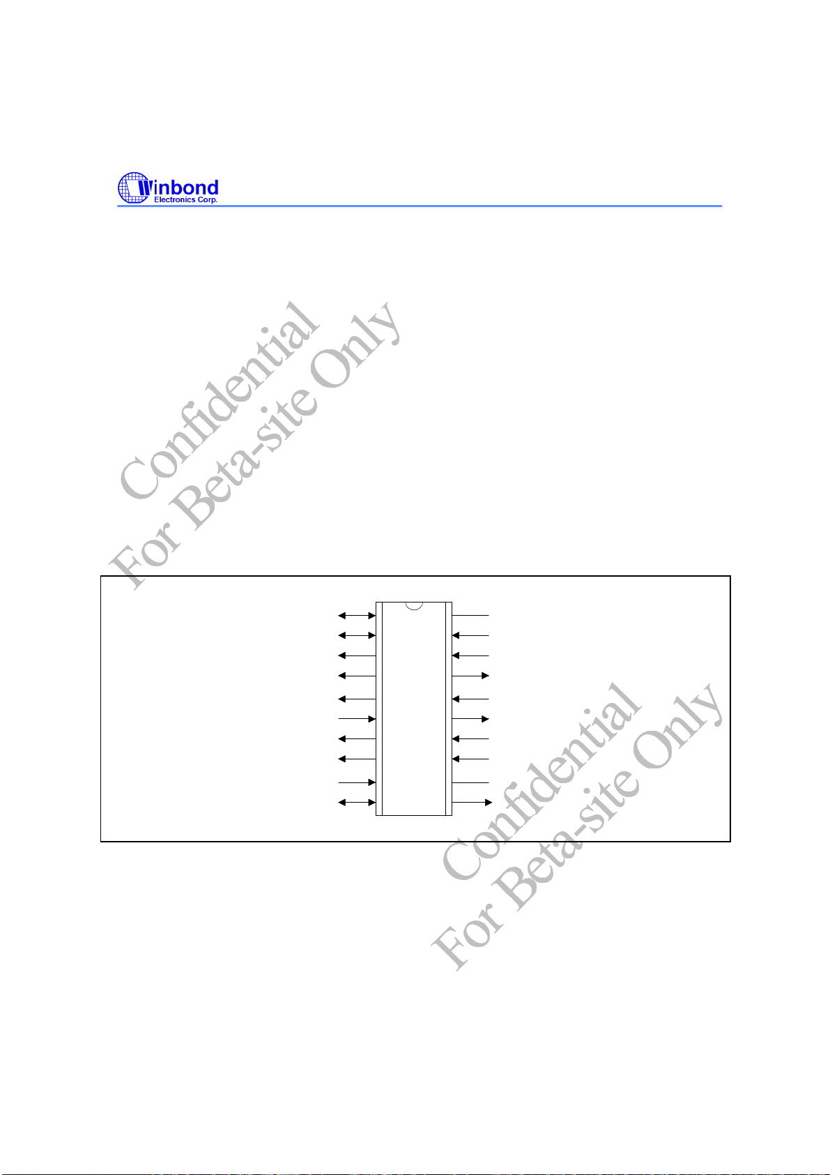
4. PIN CONFIGURATION
W83L784R
Preliminary
FANIN1/GPO1
FANIN2/GPO2
PWMOUT1
PWMOUT2
FANFAULT#/GPO3
PWR_DN#
SMI#
OVT#
SCL
SDA
10
1
2
3
4
5
6
7
8
9
20
19
18
17
16
15
14
13
12
11
VCC
CPUT1/PII1
CPUT2/PII2
VREF
VIN1
RESET#
VIN2(+3.3VIN)
VIN3(VBAT)
GND
BATFAULT#/GPO4
Confidential, For Beta-site Only Publication Release Date: Sep.
-7 - Revision 0.54
1999

5. PIN DESCRIPTION
I/O
- TTL level bi-directional pin with 12 mA source-sink capability
12t
I/O
- TTL level and schmitt trigger
12ts
OUT12 - Output pin with 12 mA source-sink capability
AOUT - Output pin(Analog)
OD12 - Open-drain output pin with 12 mA sink capability
INt - TTL level input pin
INts - TTL level input pin and schmitt trigger
AIN - Input pin(Analog)
W83L784R
Preliminary
PIN NAME PIN NO.
FANIN1 /
1 INts /
GPO1
TYPE DESCRIPTION
0V to +5V amplitude fan tachometer input. (Default) /
OUT12
General purpose output .
This multi-functional pin is programmable.
FANIN2 /
GPO2
2 INts /
OUT12
0V to +5V amplitude fan tachometer input. (Default) /
General purpose output .
This multi-functional pin is programmable.
PWMOUT1 3 OD
/
12
OUT12
Fan speed control PWM output. This pin is
default
open-drain. It
can be programmed as an output pin which can drive a HIGH or
a LOW.
PWMOUT2 4 OD
/
12
OUT12
Fan speed control PWM output. This pin is
default
open-drain. It
can be programmed as an output pin which can drive a HIGH or
a LOW.
FANFAULT# /
GPO3
5 OD12 Active-Low output. This pin will be a logic LOW when fan1 or
fan2 is abnormally stopped. (Default) /
General purpose output .
This multi-functional pin is programmable.
PWR_DN# 6
INt
Power down input. When set this pin LOW, all output pins would
be tristate except the pin15 RESET# which will keep HIGH.
SMI# 7 OD12 System Management Interrupt.
OVT# 8 OD12 Over temperature Shutdown Output.
SCL 9 INts Serial Bus Clock.
SDA 10 OD12 Serial Bus bi-directional Data.
BATFAULT#
/
GPO4
11 OD12 Active-Low output. This pin will be a logic LOW when Battery
abnormally drops below the low limit or above the high limit.
(Default) /
General purpose output .
This multi-functional pin is programmable.
GND 12 Ground Ground.
Confidential, For Beta-site Only Publication Release Date: Sep.
1999
-8 - Revision 0.54

W83L784R
Preliminary
Pin Discription, continued
PIN NAME PIN NO.
VIN3(VBAT) 13 AIN 0V to 4.096V FSR Analog Inputs. ( This pin should be
VIN2(+3.3VIN)
RESET# 15 OUT12 Active-Low reset output. RESET# remains LOW while the
VIN1(VCORE) 16 AIN 0V to 4.096V FSR Analog Inputs.
VREF 17 AOUT Reference Voltage.
CPUT2 /
PII2
CPUT1 /
PII1
VCC 20 POWER +5VCC power supply input.
14 AIN 0V to 4.096V FSR Analog Inputs. (This pin should be
18 AIN Thermistor terminal input.(Default) /
19 AIN Thermistor terminal input.(Default) /
TYPE DESCRIPTION
connected to DC BATTERY. If this voltage is above 4.096V, it
should be reduced with the external resistors so that the input
voltage will be under 4.096V. )
connected to 3VCC .)
5VCC and +3.3V are below the reset threshold. It remains
LOW for 200ms after the reset condition is terminated .
PentiumTM II diode input.
This multi-functional pin is programmable.
PentiumTM II diode input.
This multi-functional pin is programmable.
Confidential, For Beta-site Only Publication Release Date: Sep.
-9 - Revision 0.54
1999

W83L784R
Preliminary
6. FUNCTIONAL DESCRIPTION
6.1 General Description
The W83L784R provides at most 4 analog positive inputs, 2 fan speed monitors, 2 sets for
fan PWM (Pulse Width Modulation) Smart Fan Control , 2 remote thermal inputs from remote
thermistors or 2N3904 transistors or Pentium
thermal detection. W83L784R also provides the power good (reset) output for 3V and 5V power
detection and two fault output pins issuing hardware warning if battery and fans become abnormal.
When start the monitor function on the chip, the watch dog machine monitor every function and store
the value to registers. If the monitor value exceeds the limit value, the interrupt status will be set to 1.
6.2 Access Interface
The W83L784R provides I2C Serial Bus to read/write internal reigsters. In the W83L784R
there are three serial bus address. The first address defined at CR[4Ah] can read/write all registers
excluding CPUT1/CPUT2 temperature sensor registers and its address default value is 0101101. The
address for CPUT1 defined at CR[4Bh] bit2-0 only read/write CPUT1 temperature sensor registers
and the address default value is 1001001. The address for CPUT2 defined at CR[4Bh] bit2-0 only
read/write CPUT1 temperature sensor registers and the address default value is 1001000.
TM
II (Deschutes) thermal diode outputs and one on-chip
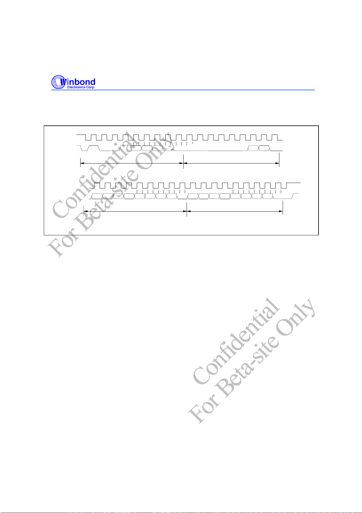
6.2.1 The first serial bus access timing are shown as follow:
(a) Serial bus write to internal address register followed by the data byte
SCL
SDA
0
0 1 0 1 1 0 1 D7 D6 D5 D4 D3 D2 D1 D0
Start By
Master
Figure 1. Serial Bus Write to Internal Address Register followed by the Data Byte
Frame 1
Serial Bus Address Byte
SCL
(Continued)
SDA (Continued)
7 8 0 7 8
R/W
Ack
by
784R
0
D7 D6 D5 D4 D3 D2 D1 D0
Frame 2
Internal Index Register Byte
Frame 3
Data Byte
7 8
784R
Ack
Stop
by
by
Master
Ack
784R
by
Confidential, For Beta-site Only Publication Release Date: Sep.
-10 - Revision 0.54
1999
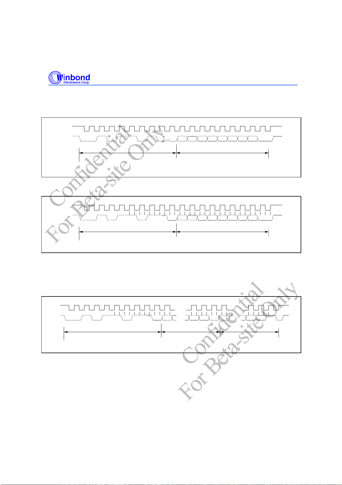
(b) Serial bus write to internal address register only
W83L784R
Preliminary
SCL
SDA
0
0 1 0 1 1 0 1 D7 D6 D5 D4 D3 D2 D1 D0
Start By
Master
Frame 1
Serial Bus Address Byte
Figure 2. Serial Bus Write to Internal Address Register Only
7 8 0 7 8
R/W
Ack
by
784R
0
Frame 2
Internal Index Register Byte
Ack
784R
Stop by
by
Master
(c) Serial bus read from a register with the internal address register prefer to desired location
SCL
SDA
0
0 1 0 1 1 0 1 D7 D6 D5 D4 D3 D2 D1 D0
Start By
Master
Frame 1
Serial Bus Address Byte
Figure 3. Serial Bus Read from Internal Address Register
7 8 0 7 8
R/W
Ack
by
784R
0
Frame 2
Internal Index Register Byte
Ack
Master
Stop by
by
Master
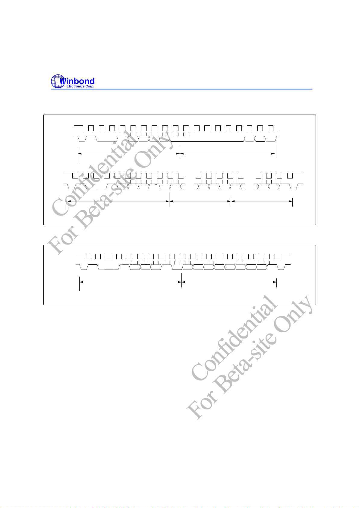
6.2.2 The serial bus timing of the temperature CPUT1 and CPUT2 is shown as follow:
(a) Typical 2-byte read from preset pointer location (Temp, TOS, T
SCL
0
7 8 0 7 8
... ...
)
HYST
0 7
SDA
0 1 0 1 1 0 1 D7 D1 D0
Start By
Master
Frame 1
Serial Bus Address Byte
Figure 4. Typical 2-Byte Read From Preset Pointer Location
R/W
Ack
784R
...
by
Frame 2
MSB Data Byte
D7 D1 D0
...
Master
Ack
by
Frame 3
LSB Data Byte
No Ack
Master
Stop by
Master
by
Confidential, For Beta-site Only Publication Release Date: Sep.
1999
-11 - Revision 0.54
W83L784R
Preliminary
(b) Typical pointer set followed by immediate read for 2-byte register (Temp, TOS, T
Frame 2
Pointer Byte
Ack
by
Master
4
D1 D0
0 7
D7 D1 D0
...
Frame 5
LSB Data Byte
Ack
784R
by
SCL
SDA
SCL
SDA
0
1 0 0 1 A2 A1 A0 R/W
Start By
Master
0
Frame 1
Serial Bus Address Byte
7 8 0
0 0 0 0 0 0
Ack
by
784R
7 8 0 7 8
... ...
1 0 0 1 A2 A1 A0 R/W
Start By
Master
Frame 3
Serial Bus Address Byte
0
Figure 5. Typical Pointer Set Followed by Immediate Read for 2-Byte Register
D7 D1 D0
...
Ack
by
784R
Frame 4
MSB Data Byte
(c) Typical read 1-byte from configuration register with preset pointer
SCL
SDA
0
1 0 0 1 A2 A1 A0 R/W D1D5 D4 D3D6
Start By
Master
Frame 1
Serial Bus Address Byte
7 8 0
D7 D2
Ack
by
782D
Frame 2
Data Byte
8
7
D0
No Ack
by
Master
HYST
No Ack
by
Master
Stop by
Master
)
Stop by
Master
Figure 6. Typical 1-Byte Read From Configuration With Preset Pointer
Confidential, For Beta-site Only Publication Release Date: Sep.
1999
-12 - Revision 0.54
W83L784R
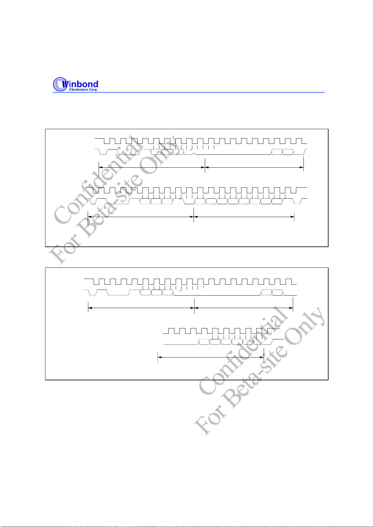
(d) Typical pointer set followed by immediate read from configuration register
Preliminary
0
1 0 0 1 A2 A1 A0 R/W
Start By
Master
0
1 0 0 1 A2 A1 A0 R/W
Serial Bus Address Byte
Frame 1
Serial Bus Address Byte
Frame 3
SCL (Cont..)
SDA (Cont..)
Repea
Start
Master
SCL
SDA
By
Figure 7. Typical Pointor Set Followed by Immediate Read from Temp 2/3 Configuration Register
(e) Temperature configuration register Write
SCL
SDA
0
1 0 0 1 A2 A1 A0 R/W
Start By
Master
Frame 1
Serial Bus Address Byte
7 8 0
0 0 0 0 00
Ack
by
784R
7 8 0
D7 D5 D4
D6 D3
Ack
by
784R
7 8 0
0 0 0 0 0 0 0
Ack
by
784R
Frame 4
MSB Data Byte
Pointer Byte
Frame 2
Frame 2
Pointer Byte
4
4
D2 D1 D0
D1 D0
D1 D0
7
No Ack
Master
7 8
7 8
8
by
Ack
by
784R
Ack
784R
...
...
by
Stop by
Master
SCL (Cont...)
SDA (Cont...)
0
0 0 D4 D3 D2 D10 D0
Configuration Data Byte
Figure 8. Configuration Register Write
Frame 3
7 8
Ack
784R
Stop
by
by
Master
Confidential, For Beta-site Only Publication Release Date: Sep.
1999
-13 - Revision 0.54
(f) Temperature TOS and T
SCL
SDA
0
1 0 0 1 A2 A1 A0 R/W
Start By
Master
Serial Bus Address Byte
HYST
Frame 1
write
7 8 0
Ack
by
784R
W83L784R
Preliminary
4
0
0
0 0 0 0
Frame 2
Pointer Byte
D1 D0
7 8
Ack
by
784R
SCL (Cont...)
SDA (Cont...)
0
D6 D5 D4 D3 D2 D1D7 D0
Frame 3
MSB Data Byte
Figure 9. Configuration Register Write
7 8
0 7 8
D6 D5 D4 D3 D2 D1D7 D0
Ack
by
784R
Frame 4
LSB Data Byte
Ack
Stop
by
by
784R
Master
Confidential, For Beta-site Only Publication Release Date: Sep.
1999
-14 - Revision 0.54

W83L784R
CPUT1
Preliminary
6.3 Analog Inputs
The maximum input voltage of the analog pin is 4.096V because the 8-bit ADC has a 16mv LSB.
Really, the application of the PC monitoring would most often be connected to power suppliers. The
CPU V-core voltage and +3.3V voltage can directly connected to these analog inputs. The 5VSB and
battery inputs should be reduced a factor with external resistors so as to obtain the input range. As
Figure 10 shows.
Positive Inputs
Typical Thermister
Connection
**The connections of CPUT2
is same as CPUT1
VIN1(VCORE)
VIN2(+3.3V)
10V(Battery DC)
R
10K, 1%
R
THM
10K, 25 C
VCC
232K, 1%
R1
VIN3(VBAT)
VREF
R2
99K, 1%
Pin 16
Pin 14
Pin 20
Pin 13
Pin 17
Pin 19
8-bit ADC
with
16mV LSB
Figure. 10.
6.3.1 Monitor over 4.096V voltage:
The input voltage VIN3 can be expressed as following equation.
R
VIN V
3
= ×
BAT DC
−
2
R R
+
1 2
The value of R1 and R2 can be selected to 232K Ohms and 99K Ohms, respectively, when the input
voltage V
is 10V. The node voltage of VIN3 can be subject to less than 4.096V for the maximun
BAT-DC
input range of the 8-bit ADC. The pin 24 is connected to the power supply VCC with +5V. There are
two functions in this pin with 5V. The first function is to supply internal analog power in the W83L784R
and the second function is that this voltage with 5V is connected to internal serial resistors to monitor
the +5V voltage. The value of two serial resistors are 34K ohms and 50K ohms so that input voltage
to ADC is 2.98V which is less than 4.096V of ADC maximum input voltage. The express equation can
represent as follows.
Confidential, For Beta-site Only Publication Release Date: Sep.
1999
-15 - Revision 0.54
W83L784R
Preliminary
K
50
V VCC
= ×
in
50 34
where VCC is set to 5V.
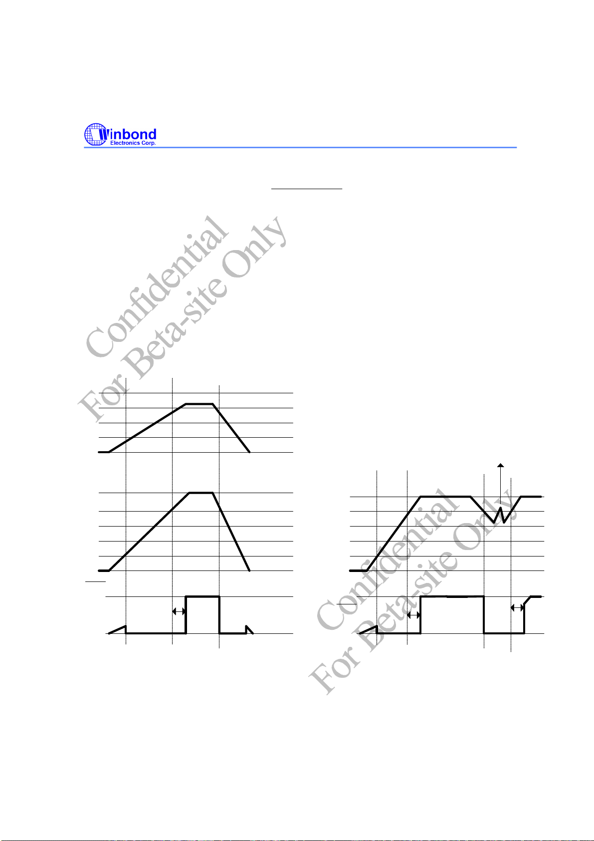
6.3.2 Power good for 3V and 5V
On power up, once VCC(5V) reaches 1V, RESET# will be a logic low. As 3V and VCC(5V)
rise, RESET# remains asserted. If 3V and VCC(5V) both exceed the reset threshold, RESET
becomes a logic high after a time equal to the reset pulse width (tRST, typically 200ms).(Figure 11).
If a power fail or a brownout happens(i.e. 3V or VCC(5V) drops below the threshold), RESET# output
is asserted. As long as the 3V and VCC(5V) remain below the reset threshold, RESET# output
remains asserted. Therefore, a brownout condition that interrupts a previously initiated reset pulse
causes an additional 200ms delay from the time the latest interruption occurred. On power-on, once
3Vor VCC(5V) drops below the reset threshold, RESET# are guaranteed to be asserted for VCC ≥ 1V.
3.3V
4
3
2
1
0
V
RST
V
RST
Ω
K K
+
Ω Ω
≅
2 98
.
V
The time of voltage over 4V
is less than tRST
VCC
5
4
3
2
1
0
RESET
V
RST
5
tRST
0
V
RST
VCC
5
4
3
2
1
0
5
RESET
0
tRST
V
RS
V
RS
Figure 11
Confidential, For Beta-site Only Publication Release Date: Sep.
1999
-16 - Revision 0.54
V
RS
tRST
 Loading...