

Winbond Electronics W83977ATF-P, W83977ATF-A Datasheet

W83977ATF
WINBOND I/O

W83977ATF
WINBOND I/O
Publication Release Date: April 1998
-1- Preliminary Revision 0.52
GENERAL DESCRIPTION
The W83977ATF is an evolving product from Winbond's most popular I/O chip W83877F --- which
integrates the disk drive adapter, serial port (UART), IrDA 1.0 SIR, parallel port, configurable plugand-play registers for the whole chip --- plus additional powerful features: ACPI, 8042 keyboard
controller with PS/2 mouse support, 23 general purpose I/O ports, full 16-bit address decoding,
OnNow keyboard wake-up, OnNow mouse wake-up, and OnNow CIR wake-up. In addition, the
W83977ATF provides IR functions: IrDA 1.1 (MIR for 1.152M bps or FIR for 4M bps) and TV remote
IR (Consumer IR, supporting NEC, RC-5, extended RC-5, and RECS-80 protocols).
The disk drive adapter functions of W83977ATF include a floppy disk drive controller compatible with
the industry standard 82077/ 765, data separator, write pre-compensation circuit, decode logic, data
rate selection, clock generator, drive interface control logic, and interrupt and DMA logic. The wide
range of functions integrated onto the W83977ATF greatly reduces the number of components
required for interfacing with floppy disk drives. The W83977ATF supports four 360K, 720K, 1.2M,
1.44M, or 2.88M disk drives and data transfer rates of 250 Kb/s, 300 Kb/s, 500 Kb/s,1 Mb/s, and 2
Mb/s.
The W83977ATF provides two high-speed serial communication ports (UARTs), one of which
supports serial Infrared communication. Each UART includes a 16-byte send/receive FIFO, a
programmable baud rate generator, complete modem control capability, and a processor interrupt
system. Both UARTs provide legacy speed with baud rate up to 115.2k bps and also advanced speed
with baud rates of 230k, 460k, or 921k bps which support higher speed modems. The W83977ATF
provides independent 3rd UART(32-byte FIFO) dedicated for the IR function.
The W83977ATF supports one PC-compatible printer port (SPP), Bi-directional Printer port (BPP)
and also Enhanced Parallel Port (EPP) and Extended Capabilities Port (ECP). Through the printer
port interface pins, also available are: Extension FDD Mode and Extension 2FDD Mode allowing one
or two external floppy disk drives to be connected.
The configuration registers support mode selection, function enable/disable, and power down function
selection. Furthermore, the configurable PnP features are compatible with the plug-and-play feature
demand of Windows 95TM, which makes system resource allocation more efficient than ever.
The W83977ATF provides functions that comply with ACPI (Advanced Configuration and Power
Interface), which includes support of legacy and ACPI power management through
SMI
or
SCI
function pins. The W83977ATF also has auto power management to reduce power consumption.
The keyboard controller is based on 8042 compatible instruction set with a 2K Byte programmable
ROM and a 256-Byte RAM bank. Keyboard BIOS firmware is available with optional AMIKEY
TM
-2,
Phoenix MultiKey/42TM, or customer code.
The W83977ATF provides a set of flexible I/O control functions to the system designer through a set
of General Purpose I/O ports. These GPIO ports may serve as simple I/O or may be individually
configured to provide a predefined alternate function.
The W83977ATF is made to fully comply with Microsoft PC97 Hardware Design Guide. IRQs,
DMAs, and I/O space resource are flexible to adjust to meet ISA PnP requirement. Moreover,
W83977ATF is made to meet the specification of PC97's requirement in the power management:
ACPI and DPM (Device Power Management).
Another benifit is that W83977ATF has the same pin assignment as W83977AF, W83977F,
W83977TF. This makes the design very flexible.

W83977ATF
PRELIMINARY
Publication Release Date: April 1998
-2- Revision 0.52
FEATURES
General
• Plug & Play 1.0A compatible
• Support 13 IRQs, 4 DMA channels, full 16-bit address decoding
• Capable of ISA Bus IRQ Sharing
• Compliant with Microsoft PC97 Hardware Design Guide
•
Support DPM (Device Power Management), ACPI
• Report ACPI status interrupt by
SCI
signal issued from any of the 13 IQRs pins or GPIO xx
• Programmable configuration settings
• Single 24/48 Mhz clock input
FDC
• Compatible with IBM PC AT disk drive systems
• Variable write pre-compensation with track selectable capability
• Support vertical recording format
• DMA enable logic
• 16-byte data FIFOs
• Support floppy disk drives and tape drives
• Detects all overrun and underrun conditions
• Built-in address mark detection circuit to simplify the read electronics
• FDD anti-virus functions with software write protect and FDD write enable signal (write data signal
was forced to be inactive)
• Support up to four 3.5-inch or 5.25-inch floppy disk drives
• Completely compatible with industry standard 82077
• 360K/720K/1.2M/1.44M/2.88M format; 250K, 300K, 500K, 1M, 2M bps data transfer rate
•
Support 3-mode FDD, and its Win95 driver
UART
• Two high-speed 16550 compatible UARTs with 16-byte send/receive FIFOs
• MIDI compatible
• Fully programmable serial-interface characteristics:
--- 5, 6, 7 or 8-bit characters
--- Even, odd or no parity bit generation/detection
--- 1, 1.5 or 2 stop bits generation
• Internal diagnostic capabilities:
--- Loop-back controls for communications link fault isolation
--- Break, parity, overrun, framing error simulation
• Programmable baud generator allows division of 1.8461 Mhz and 24 Mhz by 1 to (216-1)
• Maximum baud rate up to 921k bps for 14.769 Mhz and 1.5M bps for 24 Mhz

W83977ATF
PRELIMINARY
Publication Release Date: April 1998
-3 - Revision 0.52
Infrared
• Support IrDA version 1.0 SIR protocol with maximum baud rate up to 115.2K bps
• Support SHARP ASK-IR protocol with maximum baud rate up to 57,600 bps
• Support IrDA version 1.1 MIR (1.152M bps) and FIR (4M bps) protocol
--- Single DMA channel for transmitter or receiver
--- 3rd UART with 32-byte FIFO is supported in both TX/RX transmission
--- 8-byte status FIFO is supported to store received frame status (such as overrun CRC error,
etc.)
• Support auto-config SIR and FIR
Parallel Port
• Compatible with IBM parallel port
• Support PS/2 compatible bi-directional parallel port
• Support Enhanced Parallel Port (EPP) − Compatible with IEEE 1284 specification
• Support Extended Capabilities Port (ECP) − Compatible with IEEE 1284 specification
• Extension FDD mode supports disk drive B; and Extension 2FDD mode supports disk drives A and
B through parallel port
• Enhanced printer port back-drive current protection
Keyboard Controller
• 8042 based with optional F/W from AMIKKEYTM-2, Phoenix MultiKey/42
TM
or customer code
with 2K bytes of programmable ROM, and 256 bytes of RAM
• Asynchronous Access to Two Data Registers and One status Register
•
Software compatibility with the 8042 and PC87911 microcontrollers
• Support PS/2 mouse
• Support port 92
• Support both interrupt and polling modes
•
Fast Gate A20 and Hardware Keyboard Reset
• 8 Bit Timer/ Counter
• Support binary and BCD arithmetic
• 6MHz, 8 MHz, 12 MHz, or 16 MHz operating frequency
General Purpose I/O Ports
• 23 programmable general purpose I/O ports; 1 dedicate, 22 optional
• General purpose I/O ports can serve as simple I/O ports, interrupt steering inputs, watching dog
timer output, power LED output, infrared I/O pins, general purpose address decoder, KBC control
I/O pins

W83977ATF
PRELIMINARY
Publication Release Date: April 1998
-4- Revision 0.52
OnNow Funtions
• Keyboard wake-up by programmable keys (patent pending)
• Mouse wake-up by programmable buttons (patent pending)
• CIR wake-up by programmable keys (patent pending)
Package
• 128-pin PQFP
W83977ATF
PRELIMINARY
Publication Release Date: April 1998
-5 - Revision 0.52
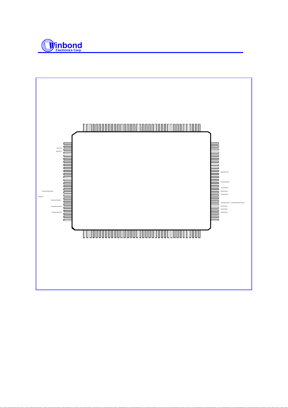
PIN CONFIGURATION
1 2 345 6
7
8
9
1
0
1
1
121
3
1
4
15161
7
181
920
2
122
2
3
2
425
2627282
9
3
031
3
2
3
3
3
4
3
5
3
6
3
7
3
8
/
M
O
P
D
7
/
A
C
K
P
D
2
P
D
3
P
D
4
/
D
I
/
S
T
P
6
V
S
S 5
/
W
E
D
/
M
O
B
A
/
W
D
Y
/
D
S
A
/
D
S
B
/
I
N
D
S
L
C
T
/
D
S
K
/
W
P
//
H
E
B
U
S
C
L
K
/
T
R
P
E
V
C
C
P
D
P
D
1
P
D
0
/
I
N
I
/
S
L
I
S
A
/
F
D
/
T
B
/
E
R
R
I
R
R
X
I
R
T
X
64
63
62
61
60
59
58
57
56
55
54
53
52
51
50
49
48
47
46
45
44
43
42
41
VBAT
XTAL1
VSS
XTAL2
MDATA
KDATA
KBLOCK/GP13
KBRST/GP12
GA20/GP11
VCC
DCDB
SOUTB/PEN48
SINB
DTRB
RTSB
DSRB
CTSB
DCDA
SOUTA/PENKBC
SINA
DTRA/PNPCSV
RTSA/HEFRAS
DSRA
CTSA
CIRRX/GP24
IRRXH/IRSL0
40
39
I
103
104
105
106
107
108
109
110
111
112
113
114
115
116
117
118
119
120
121
122
123
124
125
126
127
128
IRQ14/GP14
IRQ15/GP15
IOR
IOW
AEN
IOCHRDY
D0
D1
D2
D3
D4
D5
VCC
D6
D7
MR
DACK0/GP16
VSS
SCI/DRQ0/GP17
DACK1
DRQ1
DACK2
DRQ2
DACK3
DRQ3
TC
1
0
2
1
0
1
1
0
0
9
9
989
7
969
5949392
9
1
9089888
7
868
5
8
4
838
281807978
777
6
7
5
747
3
7
271
706
9
6
867
6
6
6
5
G
P
G
P
2
1
M
C
L
K
/
R
I
B
/
R
I
A
A
5
V
C
C
A
0
K
C
L
K
G
P
2
0
V
S
B
A1A2A3A4A6A7A8A
9
A
1
011
A
A
1
2
A
1
3
A
1
4
V
S
S
A
1
5
I
R
Q
1
2
/
S
M
I
,
222
3
G
P
I
R
Q
9
I
R
Q
8
I
R
Q
7
I
R
Q
6
I
R
Q
5
I
R
Q
4
I
R
Q
3
I
R
Q
1
I
R
Q
1
0
I
R
Q
1
1
N
D
R
V
D
E
N
0
D
R
V
D
E
N
1
,
G
P
1
0
C
H
G
A
D
D
A
T
A
A
K
0
E
P
R
E
X
N
T
R
,
/
S
C
I
,
I
N
S
W
P
A
N
O
U
S
W
P
A
N
T
,
/
/
W83977ATF
PRELIMINARY
Publication Release Date: April 1998
-6- Revision 0.52
1.0 PIN DESCRIPTION
Note: Please refer to Section 12.2 DC CHARACTERISTICS for details.
I/O6t - TTL level bi-directional pin with 6 mA source-sink capability
I/O8t - TTL level bi-directional pin with 8 mA source-sink capability
I/O8 - CMOS level bi-directional pin with 8 mA source-sink capability
I/O
12t
- TTL level bi-directional pin with 12 mA source-sink capability
I/O12 - CMOS level bi-directional pin with 12 mA source-sink capability
I/O
16u
- CMOS level bi-directional pin with 16 mA source-sink capability with internal pull-up resistor
I/OD
16u
- CMOS level bi-directional pin open drain output with 16 mA sink capability with internal pull-up resistor
I/O
24t
- TTL level bi-directional pin with 24 mA source-sink capability
OUT8t - TTL level output pin with 8 mA source-sink capability
OUT
12t
- TTL level output pin with 12 mA source-sink capability
OD12 - Open-drain output pin with 12 mA sink capability
OD24 - Open-drain output pin with 24 mA sink capability
INt - TTL level input pin
INc - CMOS level input pin
INcu - CMOS level input pin with internal pull-up resitor
INcs - CMOS level Schmitt-triggered input pin
INts - TTL level Schmitt-triggered input pin
IN
tsu
- TTL level Schmitt-triggered input pin with internal pull-up resistor
1.1 Host Interface
SYMBOL PIN I/O FUNCTION
A0−A10
74-84 IN
t
System address bus bits 0-10.
A11-A14 86-89 IN
t
System address bus bits 11-14.
A15 91 IN
t
System address bus bit 15.
D0−D5
109-
114
I/O
12t
System data bus bits 0-5.
D6−D7
116-
117
I/O
12t
System data bus bits 6-7.
IOR
105 IN
ts
CPU I/O read signal.
IOW
106 IN
ts
CPU I/O write signal.
AEN 107 IN
ts
System address bus enable.
IOCHRDY 108 OD
24
In EPP Mode, this pin is the IO Channel Ready output to extend
the host read/write cycle.
MR 118 IN
ts
Master Reset; Active high; MR is low during normal operations.
W83977ATF
PRELIMINARY
Publication Release Date: April 1998
-7 - Revision 0.52
1.1 Host Interface, continued
SYMBOL PIN I/O FUNCTION
DACK0
119 IN
tsu
DMA Channel 0 Acknowledge signal. (CR2C bit 5_4 = 00,
default)
GP16
(WDTO)
I/O
12t
General purpose I/O port 1bit 6. (CR2C bit 5_4 = 01)
Alternate function from GP16: Watch dog timer output.
P15 I/O
12t
KBC P15 I/O port. (CR2C bit 5_4 = 10)
DRQ0 121 OUT
12t
DMA Channel 0 request signal. (CR2C bit 7_6 = 00, default)
GP17
(PLEDO)
I/O
12t
General purpose I/O port 1bit 7. (CR2C bit 7_6 = 01)
Alternate Function from GP17: Power LED output.
P14 I/O
12t
KBC P14 I/O port. (CR2C bit 7_6 = 10)
SCI
OD
12
System Control Interrupt.(CR2C bit 7_6 = 11)
In the ACPI power management mode,
SCI
is driven low by the
power management events.
DACK1
122 IN
ts
DMA Channel 1 Acknowledge signal .
DRQ1 123 OUT
12t
DMA Channel 1 request signal.
DACK2
124 IN
ts
DMA Channel 2 Acknowledge signal.
DRQ2 125 OUT
12t
DMA Channel 2 request signal.
DACK3
126 IN
ts
DMA Channel 3 Acknowledge signal.
DRQ3 127 OUT
12t
DMA Channel 3 request signal.
TC 128 IN
ts
Terminal Count. When active, this pin indicates termination of a
DMA transfer.
IRQ1 99 OUT
12t
Interrupt request 1. (Logical device 9, CRF1 bit 2 = 0)
IRQ1 I/O
12t
General purpose I/O port 3 bit 0.
(Logical device 9, CRF1 bit 2 = 1)
IRQ3 98 OUT
12t
Interrupt request 3. (Logical device 9, CRF1 bit 2 = 0)
GP31 I/O
12t
General purpose I/O port 3 bit 1.
(Logical device 9, CRF1 bit 2 = 1)
IRQ4 97 OUT
12t
Interrupt request 4. (Logical device 9, CRF1 bit 2 = 0)
GP32 I/O
12t
General purpose I/O port 3 bit 2.
(Logical device 9, CRF1 bit 2 = 1)
IRQ5 96 OUT
12t
Interrupt request 5. (Logical device 9, CRF1 bit 2 = 0)
GP33 I/O
12t
General purpose I/O port 3 bit 3.
(Logical device 9, CRF1 bit 2 = 1)

W83977ATF
PRELIMINARY
Publication Release Date: April 1998
-8- Revision 0.52
1.1 Host Interface, continued
SYMBOL PIN I/O FUNCTION
IRQ6 95 OUT
12t
Interrupt request 6. (Logical device 9, CRF1 bit 2 = 0)
GP34 I/O
12t
General purpose I/O port 3 bit 4.
(Logical device 9, CRF1 bit 2 = 1)
IRQ7 94 OUT
12t
Interrupt request 7. (Logical device 9, CRF1 bit 2 = 0)
GP35 I/O
12t
General purpose I/O port 3 bit 5.
(Logical device 9, CRF1 bit 2 = 1)
IRQ8 93 OUT
12t
Interrupt request 8. (Logical device 9, CRF1 bit 2 = 0)
GP36 I/O
12t
General purpose I/O port 3 bit 6.
(Logical device 9, CRF1 bit 2 = 1)
IRQ9 92 OUT
12t
Interrupt request 9. (Logical device 9, CRF1 bit 2 = 0)
GP37 I/O
12t
General purpose I/O port 3 bit 7.
(Logical device 9, CRF1 bit 2 = 1)
IRQ10 100 OUT
12t
Interrupt request 10. (Logical device 9, CRF1 bit 2 = 0)
SERIRQ I/O
12t
Serial IRQ input/output. (Logical device 9, CRF1 bit 2 = 1)
IRQ11 101 OUT
12t
Interrupt request 11. (Logical device 9, CRF1 bit 2 = 0)
PCICLK IN
t
PCI clock input. (Logical device 9, CRF1 bit 2 = 1)
IRQ12 102 OUT
12t
Interrupt request 12. (Logical device 9, CRF1 bit 2 = 0)
GP26 I/O
12t
General purpose I/O port 2 bit 6.
(Logical device 9, CRF1 bit 2 = 1)
IRQ14 103 OUT
12t
Interrupt request 14. (CR2C bit 1_0 = 00, default)
GP14 I/O
12t
General purpose I/O port 1 bit 4. (CR2C bit 1_0 = 01)
(
GPACS
)
Alternate Function 1 from GP14: General purpose address
decode output.
(P17) Alternate Function 2 from GP14: KBC P17 I/O port.
PLEDO OUT
12t
Power LED output. (CR2C bit 1_0 = 10)
IRQ15 104 OUT
12t
Interrupt request 15.(CR2C bit 3_2 = 00, default)
GP15
(
GPAWE
)
I/O
12t
General purpose I/O port 1 bit 5. (CR2C bit 3_2 = 01)
Alternate Function 1 from GP15: General purpose address write
enable output.
(P12) Alternate Function 2 from GP15: KBC P12 I/O port.
WDT OUT
12t
Watch-Dog timer output. (CR2C bit 3_2 = 10)
CLKIN 1 IN
t
24 or 48 MHz clock input, selectable through CR24 bit 6.

W83977ATF
PRELIMINARY
Publication Release Date: April 1998
-9 - Revision 0.52
1.2 General Purpose I/O Port
SYMBOL PIN I/O FUNCTION
GP20 69 I/O
12t
General purpose I/O port 2 bit 0.
(KBRST) Alternate Function from GP20: Keyboard reset. (KBC P20)
SMI
70 OD
12
System Management Interrupt. (CR2B bit 4_3 = 00, default)
In the legacy power management mode,
SMI
is driven low by
the power managenment events.
GP21 I/O
12t
General purpose I/O port 2 bit 1. (CR2B bit 4_3 = 01)
(P13) Alternate Function from GP21: KBC P13 I/O port.
P16 I/O
12t
KBC P16 I/O port. (CR2B bit 4_3 = 10)
PANSWOUT
GP22
72 OD
12
I/O
12t
Panel Switch output. (CR2B bit 5 = 0, default)
General purpose I/O port 2 bit 2. (CR2B bit 5 = 1)
(P14) Alternate Function from GP22: KBC P14 I/O port.
PANSWIN
GP23
73 IN
12t
I/O
12t
Panel Switch input. (CR2B bit 7_6 = 00, default)
General purpose I/O port 2 bit 3. (CR2B bit 7_6 = 01)
(P15) Alternate Function from GP23: KBC P15 I/O port.
GP24 40 I/O
12t
General purpose I/O port 2 bit 4. (CR2A bit 5_4 = 01)
(P16) Alternate Function from GP24: KBC P16 I/O port.
P13 I/O
12t
KBC P13 I/O port. (CR2A bit 5_4 = 10)
CIRRX IN
t
Consumer IR receiving input. (CR2A bit 5_4 = 00)
GP25 39 I/O
12
General purpose I/O port 2 bit 5. (CR2A bit 3_2 = 10)
(GA20) Alternate Function from GP25: GATE A20. (KBC P21)
IRRXH IN
t
FIR receiving input. (CR2A bit 3_2 = 00)
IRSL0 OUT
12t
IR module select 0. (CR2A bit 3_2 = 01)
W83977ATF
PRELIMINARY
Publication Release Date: April 1998
-10- Revision 0.52
1.3 Serial Port Interface
SYMBOL PIN I/O FUNCTION
CTSA
CTSB
41
48
IN
t
Clear To Send. This is the modem control input.
The function of these pins can be tested by reading bit 4 of the
handshake status register.
DSRA
DSRB
42
49
IN
t
Data Set Ready. An active low signal indicates the modem or
data set is ready to establish a communication link and transfer
data to the UART.
RTSA
43 I/O
8t
UART A Request To Send. An active low signal informs the
modem or data set that the controller is ready to send data.
HEFRAS During power-on reset, this pin is pulled down internally and is
defined as HEFRAS, which provides the power-on value for
CR26 bit 6 (HEFRAS). A 4.7 kΩ is recommended if intends to
pull up. (select 370H as configuration I/O port′s address)
RTSB
50 I/O
8t
UART B Request To Send. An active low signal informs the
modem or data set that the controller is ready to send data.
DTRA
PNPCSV
44 I/O
8t
UART A Data Terminal Ready. An active low signal informs the
modem or data set that the controller is ready to communicate.
During power-on reset, this pin is pulled down internally and is
defined as
PNPCSV
, which provides the power-on value for
CR24 bit 0 (
PNPCSV
). A 4.7 kΩ is recommended if intends to
pull up. (clear the default value of FDC, UARTs, and PRT)
DTRB
51 I/O
8t
UART B Data Terminal Ready. An active low signal informs the
modem or data set that controller is ready to communicate.
SINA
SINB
45, 52 IN
t
Serial Input. It is used to receive serial data through the
communication link.
SOUTA 46 I/O
8t
UART A Serial Output. It is used to transmit serial data out to the
communication link.
PENKBC During power-on reset, this pin is pulled down internally and is
defined as PENKBC, which provides the power-on value for
CR24 bit 2 (ENKBC). A 4.7 kΩ resistor is recommended if
intends to pull up. (enable KBC)
SOUTB
PEN48
53 I/O
8t
UART B Serial Output. During power-on reset, this pin is pulled
down internally and is defined as PEN48, which provides the
power-on value for CR24 bit 6 (EN48). A 4.7 kΩ resistor is
recommended if intends to pull up.
DCDA
DCDB
47
54
IN
t
Data Carrier Detect. An active low signal indicates the modem
or data set has detected a data carrier.
RIA
RIB
65
66
IN
t
Ring Indicator. An active low signal indicates that a ring signal is
being received from the modem or data set.
W83977ATF
PRELIMINARY
Publication Release Date: April 1998
-11 - Revision 0.52
1.4 Infrared Interface
SYMBOL PIN I/O FUNCTION
IRRX 37 IN
cs
Infrared Receiver input.
IRTX 38 OUT
12t
Infrared Transmitter Output.
1.5 Multi-Mode Parallel Port
The following pins have alternate functions, which are controlled by CR28 and L3-CRF0.
SYMBOL PIN I/O FUNCTION
SLCT 18 IN
t
PRINTER MODE: SLCT
An active high input on this pin indicates that the printer is
selected. This pin is pulled high internally. Refer to the
description of the parallel port for definition of this pin in ECP
and EPP mode.
OD
12
EXTENSION FDD MODE:
WE
2
This pin is for Extension FDD B; its function is the same as the
WE
pin of FDC.
OD
12
EXTENSION 2FDD MODE:
WE
2
This pin is for Extension FDD A and B; its function is the same
as the WE pin of FDC.
PE 19 IN
t
PRINTER MODE: PE
An active high input on this pin indicates that the printer has
detected the end of the paper. This pin is pulled high internally.
Refer to the description of the parallel port for the definition of
this pin in ECP and EPP mode.
OD
12
EXTENSION FDD MODE:
WD
2
This pin is for Extension FDD B; its function is the same as the
WD
pin of FDC.
OD
12
EXTENSION 2FDD MODE:
WD
2
This pin is for Extension FDD A and B; its function is the same
as the WD pin of FDC.
W83977ATF
PRELIMINARY
Publication Release Date: April 1998
-12- Revision 0.52
1.5 Multi-Mode Parallel Port, continued
SYMBOL PIN I/O FUNCTION
BUSY 21 IN
t
OD
12
OD
12
PRINTER MODE: BUSY
An active high input indicates that the printer is not ready to
receive data. This pin is pulled high internally. Refer to the
description of the parallel port for definition of this pin in ECP
and EPP mode.
EXTENSION FDD MODE:
MOB
2
This pin is for Extension FDD B; its function is the same as the
MOB
pin of FDC.
EXTENSION 2FDD MODE:
MOB
2
This pin is for Extension FDD A and B; its function is the same
as the
MOB
pin of FDC.
ACK
22 IN
t
OD
12
OD
12
PRINTER MODE:
ACK
An active low input on this pin indicates that the printer has
received data and is ready to accept more data. This pin is
pulled high internally. Refer to the description of the parallel port
for the definition of this pin in ECP and EPP mode.
EXTENSION FDD MODE:
DSB
2
This pin is for the Extension FDD B; its functions is the same as
the
DSB
pin of FDC.
EXTENSION 2FDD MODE:
DSB
2
This pin is for Extension FDD A and B; its function is the same
as the
DSB
pin of FDC.
ERR
34 IN
t
OD
12
OD
12
PRINTER MODE:
ERR
An active low input on this pin indicates that the printer has
encountered an error condition. This pin is pulled high internally.
Refer to the description of the parallel port for the definition of
this pin in ECP and EPP mode.
EXTENSION FDD MODE:
HEAD
2
This pin is for Extension FDD B; its function is the same as the
HEAD
pin of FDC.
EXTENSION 2FDD MODE:
HEAD
2
This pin is for Extension FDD A and B; its function is the same
as the
HEAD
pin of FDC.
W83977ATF
PRELIMINARY
Publication Release Date: April 1998
-13 - Revision 0.52
1.5 Multi-Mode Parallel Port, continued
SYMBOL PIN I/O FUNCTION
SLIN
32 OD
12
OD
12
OD
12
PRINTER MODE:
SLIN
Output line for detection of printer selection. This pin is pulled
high internally. Refer to the description of the parallel port for
the definition of this pin in ECP and EPP mode.
EXTENSION FDD MODE:
STEP
2
This pin is for Extension FDD B; its function is the same as the
STEP
pin of FDC.
EXTENSION 2FDD MODE:
STEP
2
This pin is for Extension FDD A and B; its function is the same
as the
STEP
pin of FDC.
INIT
33 OD
12
OD
12
OD
12
PRINTER MODE:
INIT
Output line for the printer initialization. This pin is pulled high
internally. Refer to the description of the parallel port for the
definition of this pin in ECP and EPP mode.
EXTENSION FDD MODE:
DIR
2
This pin is for Extension FDD B; its function is the same as the
DIR
pin of FDC.
EXTENSION 2FDD MODE:
DIR
2
This pin is for Extension FDD A and B; its function is the same
as the
DIR
pin of FDC.
AFD
35 OD
12
OD
12
OD
12
PRINTER MODE:
AFD
An active low output from this pin causes the printer to auto feed
a line after a line is printed. This pin is pulled high internally.
Refer to the description of the parallel port for the definition of
this pin in ECP and EPP mode.
EXTENSION FDD MODE: DRVDEN0
This pin is for Extension FDD B; its function is the same as the
DRVDEN0 pin of FDC.
EXTENSION 2FDD MODE: DRVDEN0
This pin is for Extension FDD A and B; its function is the same
as the DRVDEN0 pin of FDC.
STB
36 OD
12
PRINTER MODE:
STB
An active low output is used to latch the parallel data into the
printer. This pin is pulled high internally. Refer to the description
of the parallel port for the definition of this pin in ECP and EPP
mode.
- EXTENSION FDD MODE: This pin is a tri-state output.
- EXTENSION 2FDD MODE: This pin is a tri-state output.

W83977ATF
PRELIMINARY
Publication Release Date: April 1998
-14- Revision 0.52
1.5 Multi-Mode Parallel Port, continued
SYMBOL PIN I/O FUNCTION
PD0 31 I/O
24t
PRINTER MODE: PD0
Parallel port data bus bit 0. Refer to the description of the
parallel port for the definition of this pin in ECP and EPP mode.
IN
t
EXTENSION FDD MODE:
INDEX
2
This pin is for Extension FDD B; its function is the same as the
INDEX
pin of FDC. It is pulled high internally.
IN
t
EXTENSION 2FDD MODE:
INDEX
2
This pin is for Extension FDD A and B; its function is the same
as the
INDEX
pin of FDC. It is pulled high internally.
PD1 30 I/O
24t
IN
t
IN
t
PRINTER MODE: PD1
Parallel port data bus bit 1. Refer to the description of the
parallel port for the definition of this pin in ECP and EPP mode.
EXTENSION FDD MODE:
TRAK
02
This pin is for Extension FDD B; its function is the same as the
TRAK
0
pin of FDC. It is pulled high internally.
EXTENSION. 2FDD MODE:
TRAK
02
This pin is for Extension FDD A and B; its function is the same
as the
TRAK
0
pin of FDC. It is pulled high internally.
PD2 29 I/O
24t
IN
t
IN
t
PRINTER MODE: PD2
Parallel port data bus bit 2. Refer to the description of the
parallel port for the definition of this pin in ECP and EPP mode.
EXTENSION FDD MODE:
WP
2
This pin is for Extension FDD B; its function is the same as the
WP
pin of FDC. It is pulled high internally.
EXTENSION. 2FDD MODE:
WP
2
This pin is for Extension FDD A and B; its function is the same
as the WP pin of FDC. It is pulled high internally.
PD3 28 I/O
24t
IN
t
IN
t
PRINTER MODE: PD3
Parallel port data bus bit 3. Refer to the description of the
parallel port for the definition of this pin in ECP and EPP mode.
EXTENSION FDD MODE:
RDATA
2
This pin is for Extension FDD B; its function is the same as the
RDATA
pin of FDC. It is pulled high internally.
EXTENSION 2FDD MODE:
RDATA
2
This pin is for Extension FDD A and B; its function is the same
as the
RDATA
pin of FDC. It is pulled high internally.
W83977ATF
PRELIMINARY
Publication Release Date: April 1998
-15 - Revision 0.52
1.5 Multi-Mode Parallel Port, continued
SYMBOL PIN I/O FUNCTION
PD4 27 I/O
24t
IN
t
IN
t
PRINTER MODE: PD4
Parallel port data bus bit 4. Refer to the description of the
parallel port for the definition of this pin in ECP and EPP mode.
EXTENSION FDD MODE:
DSKCHG
2
This pin is for Extension FDD B; the function of this pin is the
same as the
DSKCHG
pin of FDC. It is pulled high internally.
EXTENSION 2FDD MODE:
DSKCHG
2
This pin is for Extension FDD A and B; this function of this pin is
the same as the
DSKCHG
pin of FDC. It is pulled high internally.
PD5 26 I/O
24t
-
-
PRINTER MODE: PD5
Parallel port data bus bit 5. Refer to the description of the
parallel port for the definition of this pin in ECP and EPP mode.
EXTENSION FDD MODE: This pin is a tri-state output.
EXTENSION 2FDD MODE: This pin is a tri-state output.
PD6 24 I/O
24t
-
OD
24
PRINTER MODE: PD6
Parallel port data bus bit 6. Refer to the description of the
parallel port for the definition of this pin in ECP and EPP mode.
EXTENSION FDD MODE: This pin is a tri-state output.
EXTENSION. 2FDD MODE:
MOA
2
This pin is for Extension FDD A; its function is the same as the
MOA
pin of FDC.
PD7 23 I/O
24t
-
OD
24
PRINTER MODE: PD7
Parallel port data bus bit 7. Refer to the description of the
parallel port for the definition of this pin in ECP and EPP mode.
EXTENSION FDD MODE: This pin is a tri-state output.
EXTENSION 2FDD MODE:
DSA
2
This pin is for Extension FDD A; its function is the same as the
DSA
pin of FDC.
W83977ATF
PRELIMINARY
Publication Release Date: April 1998
-16- Revision 0.52
1.6 FDC Interface
SYMBOL PIN I/O FUNCTION
DRVDEN0 2 OD
24
Drive Density Select bit 0.
DRVDEN1 3 OD
24
Drive Density Select bit 1. (CR2A bit 1_0 = 00, default)
GP10 IO
24t
General purpose I/O port 1 bit 0. (CR2A bit 1_0 = 01)
(IRQIN1) Alternate Function from GP10: Interrupt channel input.
P12 IO
24t
KBC P12 I/O port. (CR2A bit 1_0 = 10)
SCI
OD
12
System Control Interrupt. (CR2A bit 1_0 = 11)
In the ACPI power management mode,
SCI
is driven low by the
power management events.
HEAD
5 OD
24
Head select. This open drain output determines which disk drive
head is active.
Logic 1 = side 0
Logic 0 = side 1
WE
9 OD
24
Write enable. An open drain output.
WD
10 OD
24
Write data. This logic low open drain writes pre-compensation
serial data to the selected FDD. An open drain output.
STEP
11 OD
24
Step output pulses. This active low open drain output produces
a pulse to move the head to another track.
DIR
12 OD
24
Direction of the head step motor. An open drain output.
Logic 1 = outward motion
Logic 0 = inward motion
MOB
13 OD
24
Motor B On. When set to 0, this pin enables disk drive 1. This is
an open drain output.
DSA
14 OD
24
Drive Select A. When set to 0, this pin enables disk drive A.
This is an open drain output.
DSB
15 OD
24
Drive Select B. When set to 0, this pin enables disk drive B.
This is an open drain output.
MOA
16 OD
24
Motor A On. When set to 0, this pin enables disk drive 0. This is
an open drain output.
DSKCHG
4 IN
cs
Diskette change. This signal is active low at power on and
whenever the diskette is removed. This input pin is pulled up
internally by a 1 KΩ resistor. The resistor can be disabled by bit
7 of L0-CRF0 (FIPURDWN).

W83977ATF
PRELIMINARY
Publication Release Date: April 1998
-17 - Revision 0.52
1.6 FDC Interface, continued
SYMBOL PIN I/O FUNCTION
RDATA
6 IN
cs
The read data input signal from the FDD. This input pin is pulled
up internally by a 1 KΩ resistor. The resistor can be disabled by
bit 7 of L0-CRF0 (FIPURDWN).
WP
7 IN
cs
Write protected. This active low Schmitt input from the disk
drive indicates that the diskette is write-protected. This input pin
is pulled up internally by a 1 KΩ resistor. The resistor can be
disabled by bit 7 of L0-CRF0 (FIPURDWN).
TRAK0
8 IN
cs
Track 0. This Schmitt-triggered input from the disk drive is
active low when the head is positioned over the outermost track.
This input pin is pulled up internally by a 1 KΩ resistor. The
resistor can be disabled by bit 7 of L0-CRF0 (FIPURDWN).
INDEX
17 IN
cs
This Schmitt-triggered input from the disk drive is active low
when the head is positioned over the beginning of a track
marked by an index hole. This input pin is pulled up internally by
a 1 KΩ resistor. The resistor can be disabled by bit 7 of L0-CRF0
(FIPURDWN).
1.7 KBC Interface
SYMBOL PIN I/O FUNCTION
KDATA 59 I/O
16u
Keyboard Data.
MDATA 60 I/O
16u
PS2 Mouse Data.
KCLK 67 I/O
16u
Keyboard Clock.
MCLK 68 I/O
16u
PS2 Mouse Clock.
GA20 56 I/O
12t
KBC GATE A20 (P21) Output. (CR2A bit 6 = 0, default)
GP11 I/O
12t
General purpose I/O port 1 bit 1. (CR2A bit 6 = 1)
(IRQIN2) Alternate Function from GP11: Interrupt channel input.
KBRST 57 I/O
12t
W83C45 Keyboard Reset (P20) Output. (CR2A bit 7 = 0, default)
GP12 I/O
12t
General purpose I/O port 1 bit 2. (CR2A bit 7 = 1)
(WDTO) Alternate Function 1 from GP12 : Watchdog timer output.
KBLOCK 58 IN
ts
W83C45 KINH (P17) Input. (CR2B bit 0 = 0, default)
GP13 I/O
16t
General purpose I/O port 1 bit 3. (CR2B bit 0 = 1)

W83977ATF
PRELIMINARY
Publication Release Date: April 1998
-18- Revision 0.52
1.8 POWER PINS
SYMBOL PIN FUNCTION
VCC 20, 55, 85,
115
+5V power supply for the digital circuitry.
VSB 71 +5V stand-by power supply for the digital circuitry.
GND 25, 62, 90,
120
Ground.
1.9 ACPI Interface
SYMBOL PIN I/O FUNCTION
VBAT 64 NA Battery voltage input.
XTAL1 63 IN
C
32.768Khz Clock Input.
XTAL2 61 O
8t
32.768Khz Clock Output.

W83977ATF
PRELIMINARY
Publication Release Date: April 1998
-19 - Revision 0.52
2.0 FDC FUNCTIONAL DESCRIPTION
2.1 W83977ATF FDC
The floppy disk controller of the W83977ATF integrates all of the logic required for floppy disk
control. The FDC implements a PC/AT or PS/2 solution. All programmable options default to
compatible values. The FIFO provides better system performance in multi-master systems. The
digital data separator supports up to 2 M bits/sec data rate.
The FDC includes the following blocks: AT interface, Precompensation, Data Rate Selection, Digital
Data Separator, FIFO, and FDC Core.
2.1.1 AT interface
The interface consists of the standard asynchronous signals: RD, WR, A0-A3, IRQ, DMA control,
and a data bus. The address lines select between the configuration registers, the FIFO and
control/status registers. This interface can be switched between PC/AT, Model 30, or PS/2 normal
modes. The PS/2 register sets are a superset of the registers found in a PC/AT.
2.1.2 FIFO (Data)
The FIFO is 16 bytes in size and has programmable threshold values. All command parameter
information and disk data transfers go through the FIFO. Data transfers are governed by the RQM
and DIO bits in the Main Status Register.
The FIFO defaults to disabled mode after any form of reset. This maintains PC/AT hardware
compatibility. The default values can be changed through the CONFIGURE command. The
advantage of the FIFO is that it allows the system a larger DMA latency without causing disk errors.
The following tables give several examples of the delays with a FIFO. The data are based upon the
following formula:
THRESHOLD # × (1/DATA/RATE) *8 - 1.5 µS = DELAY
FIFO THRESHOLD MAXIMUM DELAY TO SERVICING AT 500K BPS
Data Rate
1 Byte
1 × 16 µS - 1.5 µS = 14.5 µS
2 Byte
2 × 16 µS - 1.5 µS = 30.5 µS
8 Byte
8 × 16 µS - 1.5 µS = 6.5 µS
15 Byte
15 × 16 µS - 1.5 µS = 238.5 µS
FIFO THRESHOLD MAXIMUM DELAY TO SERVICING AT 1M BPS
Data Rate
1 Byte
1 × 8 µS - 1.5 µS = 6.5 µS
2 Byte
2 × 8 µS - 1.5 µS = 14.5 µS
8 Byte
8 × 8 µS - 1.5 µS = 62.5 µS
15 Byte
15 × 8 µS - 1.5 µS = 118.5 µS

W83977ATF
PRELIMINARY
Publication Release Date: April 1998
-20- Revision 0.52
At the start of a command the FIFO is always disabled, and command parameters must be sent
based upon the RQM and DIO bit settings in the main status register. When the FDC enters the
command execution phase, it clears the FIFO of any data to ensure that invalid data are not
transferred.
An overrun and underrun will terminate the current command and the data transfer. Disk writes will
complete the current sector by generating a 00 pattern and valid CRC. Reads require the host to
remove the remaining data so that the result phase may be entered.
DMA transfers are enabled with the SPECIFY command and are initiated by the FDC by activating
the DRQ pin during a data transfer command. The FIFO is enabled directly by asserting
DACK
and
addresses need not be valid.
Note that if the DMA controller is programmed to function in verify mode a pseudo read is performed
by the FDC based only on
DACK
. This mode is only available when the FDC has been configured
into byte mode (FIFO disabled) and is programmed to do a read. With the FIFO enabled the above
operation is performed by using the new VERIFY command. No DMA operation is needed.¡ @
2.1.3 Data Separator
The function of the data separator is to lock onto the incoming serial read data. When a lock is
achieved the serial front end logic of the chip is provided with a clock which is synchronized to the
read data. The synchronized clock, called the Data Window, is used to internally sample the serial
data portion of the bit cell, and the alternate state samples the clock portion. Serial to parallel
conversion logic separates the read data into clock and data bytes.
The Digital Data Separator (DDS) has three parts: control logic, error adjustment, and speed tracking.
Ideally, the DDS circuit cycles once every 12 clock cycles. Any data pulse input will be synchronized
and then adjusted by immediate error adjustment. The control logic will generate RDD and RWD for
every pulse input. During any cycle where no data pulse is present, the DDS cycles are based on
speed. A digital integrator is used to keep track of the speed changes in the input data stream.
2.1.4 Write Precompensation
The write precompensation logic is used to minimize bit shifts in the RDDATA stream from the disk
drive. Shifting of bits is a known phenomenon in magnetic media and is dependent on the disk media
and the floppy drive.
The FDC monitors the bit stream that is being sent to the drive. The data patterns that require
precompensation are well known. Depending upon the pattern, the bit is shifted either early or late
relative to the surrounding bits.
2.1.5 Perpendicular Recording Mode
The FDC is also capable of interfacing directly to perpendicular recording floppy drives. Perpendicular
recording differs from the traditional longitudinal method in that the magnetic bits are oriented
vertically. This scheme packs more data bits into the same area.
FDCs with perpendicular recording drives can read standard 3.5" floppy disks, and can also read and
write perpendicular media. Some manufacturers offer drives that can read and write standard and
perpendicular media in a perpendicular media drive.
A single command puts the FDC into perpendicular mode. All other commands operate as they
normally do. The perpendicular mode requires a 1 Mbps data rate for the FDC. At this data rate the
FIFO eases the host interface bottleneck due to the speed of data transfer to or from the disk.

W83977ATF
PRELIMINARY
Publication Release Date: April 1998
-21 - Revision 0.52
2.1.6 FDC Core
The W83977ATF FDC is capable of performing twenty commands. Each command is initiated by a
multi-byte transfer from the microprocessor. The result can also be a multi-byte transfer back to the
microprocessor. Each command consists of three phases: command, execution, and result.
Command
The microprocessor issues all required information to the controller to perform a specific operation.
Execution
The controller performs the specified operation.
Result
After the operation is completed, status information and other housekeeping information is provided
to the microprocessor.
2.1.7 FDC Commands
Command Symbol Descriptions:
C: Cylinder number 0 - 256
D: Data Pattern
DIR: Step Direction
DIR = 0, step out
DIR = 1, step in
DS0: Disk Drive Select 0
DS1: Disk Drive Select 1
DTL: Data Length
EC: Enable Count
EOT: End of Track
EFIFO: Enable FIFO
EIS: Enable Implied Seek
EOT: End of track
FIFOTHR: FIFO Threshold
GAP: Gap length selection
GPL: Gap Length
H: Head number
HDS: Head number select
HLT: Head Load Time
HUT: Head Unload Time
LOCK: Lock EFIFO, FIFOTHR, PTRTRK bits prevent affected by software reset
MFM: MFM or FM Mode
MT: Multitrack
N: The number of data bytes written in a sector
NCN: New Cylinder Number
ND: Non-DMA Mode
OW: Overwritten
PCN: Present Cylinder Number

W83977ATF
PRELIMINARY
Publication Release Date: April 1998
-22- Revision 0.52
POLL: Polling Disable
PRETRK: Precompensation Start Track Number
R: Record
RCN: Relative Cylinder Number
R/W: Read/Write
SC: Sector/per cylinder
SK: Skip deleted data address mark
SRT: Step Rate Time
ST0: Status Register 0
ST1: Status Register 1
ST2: Status Register 2
ST3: Status Register 3
WG: Write gate alters timing of WE
(1) Read Data
PHASE R/W D7 D6 D5 D4 D3 D2 D1 D0 REMARKS
Command W MT MFM SK 0 0 1 1 0 Command codes
W 0 0 0 0 0 HDS DS1 DS0
W
W
---------------------- C ------------------------
---------------------- H ------------------------
Sector ID information prior
to command execution
W
W
---------------------- R ------------------------
---------------------- N -----------------------W
W
-------------------- EOT -----------------------
-------------------- GPL -----------------------
W -------------------- DTL -----------------------
Execution Data transfer between the
FDD and system
Result R
R
R
-------------------- ST0 -----------------------
-------------------- ST1 -----------------------
-------------------- ST2 -----------------------
Status information after
command execution
R
R
R
R
---------------------- C ------------------------
---------------------- H ------------------------
---------------------- R ------------------------
---------------------- N ------------------------
Sector ID information after
command execution

W83977ATF
PRELIMINARY
Publication Release Date: April 1998
-23 - Revision 0.52
(2) Read Deleted Data
PHASE R/W D7 D6 D5 D4 D3 D2 D1 D0 REMARKS
Command W MT MFM SK 0 1 1 0 0 Command codes
W 0 0 0 0 0 HDS DS1 DS0
W
W
---------------------- C ------------------------
---------------------- H ------------------------
Sector ID information prior
to command execution
W
W
---------------------- R ------------------------
---------------------- N -----------------------W
W
-------------------- EOT -----------------------
-------------------- GPL -----------------------
W -------------------- DTL -----------------------
Execution Data transfer between the
FDD and system
Result R
R
R
-------------------- ST0 -----------------------
-------------------- ST1 -----------------------
-------------------- ST2 -----------------------
Status information after
command execution
R
R
R
R
---------------------- C ------------------------
---------------------- H ------------------------
---------------------- R ------------------------
---------------------- N ------------------------
Sector ID information after
command execution

W83977ATF
PRELIMINARY
Publication Release Date: April 1998
-24- Revision 0.52
(3) Read A Track
PHASE R/W D7 D6 D5 D4 D3 D2 D1 D0 REMARKS
Command W 0 MFM 0 0 0 0 1 0 Command codes
W 0 0 0 0 0 HDS DS1 DS0
W
W
---------------------- C ------------------------
---------------------- H ------------------------
Sector ID information prior
to command execution
W
W
---------------------- R ------------------------
---------------------- N -----------------------W
W
-------------------- EOT -----------------------
-------------------- GPL -----------------------
W -------------------- DTL -----------------------
Execution Data transfer between the
FDD and system; FDD
reads contents of all
cylinders from index hole to
EOT
Result R
R
R
-------------------- ST0 -----------------------
-------------------- ST1 -----------------------
-------------------- ST2 -----------------------
Status information after
command execution
R
R
R
R
---------------------- C ------------------------
---------------------- H ------------------------
---------------------- R ------------------------
---------------------- N ------------------------
Sector ID information after
command execution

W83977ATF
PRELIMINARY
Publication Release Date: April 1998
-25 - Revision 0.52
(4) Read ID
PHASE R/W D7 D6 D5 D4 D3 D2 D1 D0 REMARKS
Command W 0 MFM 0 0 1 0 1 0 Command codes
W 0 0 0 0 0 HDS DS1 DS0
Execution The first correct ID
information on the cylinder
is stored in Data Register
Result R
R
R
-------------------- ST0 -----------------------
-------------------- ST1 -----------------------
-------------------- ST2 -----------------------
Status information after
command execution
R
R
R
R
---------------------- C ------------------------
---------------------- H ------------------------
---------------------- R ------------------------
---------------------- N ------------------------
Disk status after the
command has been
completed
(5) Verify
PHASE R/W D7 D6 D5 D4 D3 D2 D1 D0 REMARKS
Command W MT MFM SK 1 0 1 1 0 Command codes
W EC 0 0 0 0 HDS DS1 DS0
W
W
---------------------- C ------------------------
---------------------- H ------------------------
Sector ID information prior
to command execution
W
W
---------------------- R ------------------------
---------------------- N -----------------------W
W
-------------------- EOT -----------------------
-------------------- GPL -----------------------
-------------------- DTL/SC -------------------
Execution No data transfer takes
place
Result R
R
R
-------------------- ST0 -----------------------
-------------------- ST1 -----------------------
-------------------- ST2 -----------------------
Status information after
command execution
R
R
R
R
---------------------- C ------------------------
---------------------- H ------------------------
---------------------- R ------------------------
---------------------- N ------------------------
Sector ID information after
command execution

W83977ATF
PRELIMINARY
Publication Release Date: April 1998
-26- Revision 0.52
(6) Version
PHASE R/W D7 D6 D5 D4 D3 D2 D1 D0 REMARKS
Command W 0 0 0 1 0 0 0 0 Command code
Result R 1 0 0 1 0 0 0 0 Enhanced controller
(7) Write Data
PHASE R/W D7 D6 D5 D4 D3 D2 D1 D0 REMARKS
Command W MT MFM 0 0 0 1 0 1 Command codes
W 0 0 0 0 0 HDS DS1 DS0
W
W
---------------------- C ------------------------
---------------------- H ------------------------
Sector ID information prior
to Command execution
W
W
---------------------- R ------------------------
---------------------- N -----------------------W
W
-------------------- EOT -----------------------
-------------------- GPL -----------------------
W -------------------- DTL -----------------------
Execution Data transfer between the
FDD and system
Result R
R
R
-------------------- ST0 -----------------------
-------------------- ST1 -----------------------
-------------------- ST2 -----------------------
Status information after
Command execution
R
R
R
R
---------------------- C ------------------------
---------------------- H ------------------------
---------------------- R ------------------------
---------------------- N ------------------------
Sector ID information after
Command execution

W83977ATF
PRELIMINARY
Publication Release Date: April 1998
-27 - Revision 0.52
(8) Write Deleted Data
PHASE R/W D7 D6 D5 D4 D3 D2 D1 D0 REMARKS
Command W MT MFM 0 0 1 0 0 1 Command codes
W 0 0 0 0 0 HDS DS1 DS0
W
W
---------------------- C ------------------------
---------------------- H ------------------------
Sector ID information prior
to command execution
W
W
---------------------- R ------------------------
---------------------- N -----------------------W
W
W
-------------------- EOT -----------------------
-------------------- GPL -----------------------
-------------------- DTL -----------------------
Execution Data transfer between the
FDD and system
Result R
R
R
-------------------- ST0 -----------------------
-------------------- ST1 -----------------------
-------------------- ST2 -----------------------
Status information after
command execution
R
R
R
R
---------------------- C ------------------------
---------------------- H ------------------------
---------------------- R ------------------------
---------------------- N ------------------------
Sector ID information after
command execution

W83977ATF
PRELIMINARY
Publication Release Date: April 1998
-28- Revision 0.52
(9) Format A Track
PHASE R/W D7 D6 D5 D4 D3 D2 D1 D0 REMARKS
Command W 0 MFM 0 0 1 1 0 1 Command codes
W 0 0 0 0 0 HDS DS1 DS0
W
W
---------------------- N ------------------------
--------------------- SC -----------------------
Bytes/Sector
Sectors/Cylinder
W
W
--------------------- GPL ---------------------
---------------------- D ------------------------
Gap 3
Filler Byte
Execution
for Each
Sector
Repeat:
W
W
W
W
---------------------- C ------------------------
---------------------- H ------------------------
---------------------- R ------------------------
---------------------- N ------------------------
Input Sector Parameters
Result R
R
R
-------------------- ST0 -----------------------
-------------------- ST1 -----------------------
-------------------- ST2 -----------------------
Status information after
command execution
R
R
R
R
---------------- Undefined -------------------
---------------- Undefined -------------------
---------------- Undefined -------------------
---------------- Undefined -------------------
(10) Recalibrate
PHASE R/W D7 D6 D5 D4 D3 D2 D1 D0 REMARKS
Command W 0 0 0 0 0 1 1 1 Command codes
W 0 0 0 0 0 0 DS1 DS0
Execution Head retracted to Track 0
Interrupt
(11) Sense Interrupt Status
PHASE R/W D7 D6 D5 D4 D3 D2 D1 D0 REMARKS
Command W 0 0 0 0 1 0 0 0 Command code
Result R
R
---------------- ST0 -------------------------
---------------- PCN -------------------------
Status information at the end
of each seek operation

W83977ATF
PRELIMINARY
Publication Release Date: April 1998
-29 - Revision 0.52
(12) Specify
PHASE R/W D7 D6 D5 D4 D3 D2 D1 D0 REMARKS
Command W 0 0 0 0 0 0 1 1 Command codes
W
W
| ---------SRT ----------- | --------- HUT ---------- |
|------------ HLT ----------------------------------| ND
(13) Seek
PHASE R/W D7 D6 D5 D4 D3 D2 D1 D0 REMARKS
Command W 0 0 0 0 1 1 1 1 Command codes
WW 0 0 0 0 0 HDS DS1 DS0
-------------------- NCN -----------------------
Execution R Head positioned over proper
cylinder on diskette
(14) Configure
PHASE R/W D7 D6 D5 D4 D3 D2 D1 D0 REMARKS
Command W 0 0 0 1 0 0 1 1 Configure information
W
W
W
0 0 0 0 0 0 0 0
0 EIS EFIFO POLL | ------ FIFOTHR ----|
| --------------------PRETRK ----------------------- |
Execution Internal registers written
(15) Relative Seek
PHASE R/W D7 D6 D5 D4 D3 D2 D1 D0 REMARKS
Command W 1 DIR 0 0 1 1 1 1 Command codes
WW 0 0 0 0 0 HDS DS1 DS0
| -------------------- RCN ---------------------------- |
 Loading...