

Winbond Electronics W83877F Datasheet

W83877F
WINBOND I/O
GENERAL DESCRIPTION
One of Winbond's popular series of I/O chips, the W83877F integrates a disk drive adapter, serial
port (UART), parallel port, IDE bus interface, and game port decoder onto a single chip. The
W83877F is an enhanced version of the W83777F, with additional powerful features such as
configurable plug-and-play registers for the whole chip and infrared support in one of the serial ports.
The disk drive adapter functions of the W83877F include a floppy disk drive controller compatible
with the industry standard 82077/765, data separator, write pre-compensation circuit, decode logic,
data rate selection, clock generator, drive interface control logic, and interrupt and DMA logic. The
wide range of functions integrated onto the W83877F greatly reduces the number of components
required for interfacing with floppy disk drives. The W83877F supports four 360K, 720K, 1.2M, 1.44M,
or 2.88M disk drives and data transfer rates of 250 Kb/S, 300 Kb/S, 500 Kb/S, and 1 Mb/S.
The W83877F provides two high-speed serial communication ports (UARTs), one of which supports
serial Infrared communication. Each UART includes a 16-byte send/receive FIFO, a programmable
baud rate generator, complete modem control capability, and a processor interrupt system.
The W83877F supports one PC-compatible printer port. Additional bidirectional I/O capability is
available by hardware control or software programming. The parallel port also supports the Enhanced
Parallel Port (EPP) and Extended Capabilities Port (ECP).
The W83877F supports two embedded hard disk drive (AT bus) interfaces and a game port with
decoded read/write output. The chip's Extension FDD Mode and Extension 2FDD Mode allow one or
two external floppy disk drives to be connected to the computer through the printer interface pins in
notebook computer applications.
The Extension Adapter Mode of the W83877F allows pocket devices to be installed through the
printer interface pins in notebook computer applications according to a protocol set by Winbond, but
with upgraded performance. The JOYSTICK mode allows a joystick to be connected to a parallel port
with a signal switching cable.
The configuration registers support mode selection, function enable/disable, and power down function
selection. Moreover, the configurable PnP registers are compatible with the plug-and-play feature in
Windows 95
TM
, which makes system resource allocation more efficient than ever.
Publication Release Date: January 1996
- 1 - Revision A2

W83877F
FEATURES
FDC:
• Compatible with IBM PC AT disk drive systems
• Variable write pre-compensation with track selectable capability
• DMA enable logic
• Non-burst mode DMA option
• Supports floppy disk drives and tape drives
• Detects all overrun and underrun conditions
• Data rate and drive control registers
• Built-in address mark detection circuit to simplify the read electronics
• IBM PC system address decoder
• Supports up to two embedded hard disk drives (IDE AT BUS)
• Single 24 MHz crystal input
• FDD anti-virus functions with software write protect and FDD write enable signal, write data signal
force inactive
• Supports up to four 3.5-inch or 5.25-inch floppy disk drives
• Completely compatible with industry standard 82077
• 360K/720K/1.2M/1.44M/2.88M format
• 250K, 300K, 500K, 1M bps data transfer rate
• Supports vertical recording format
• 16-byte data FIFOs
UART:
• Two high-speed 16550 compatible UARTs with 16-byte send/receive FIFOs
• MIDI compatible
• Fully programmable serial-interface characteristics:
− 5, 6, 7 or 8-bit characters
− Even, odd or no parity bit generation/detection
− 1, 1.5 or 2 stop bits generation
• Internal diagnostic capabilities:
− Loop-back controls for communications link fault isolation
− Break, parity, overrun, framing error simulation
• Programmable baud generator allows division of 1.8461 MHz and 24 MHz by 1 to (2
Parallel Port:
- 2 -
16
-1)

W83877F
• Compatible with IBM parallel port
• Supports parallel port with bidirectional lines
• Supports Enhanced Parallel Port (EPP)
− Compatible with IEEE 1284 specification
• Supports Extended Capabilities Port (ECP)
− Compatible with IEEE 1284 specification
• Extension FDD mode supports disk drive B through parallel port
• Extension Adapter Mode supports pocket devices through parallel port
• Extension 2FDD mode supports disk drives A and B through parallel port
• JOYSTICK mode supports joystick through parallel port
Others:
• Programmable configuration settings
• Immediate or automatic power-down mode for power management
• All hardware power-on settings have internal pull-up or pull-down resistors as default value
• Packaged in 100-pin QFP
• Configurable Plug and Play registers
• Infrared communication port
Publication Release Date: January 1996
- 3 - Revision A2
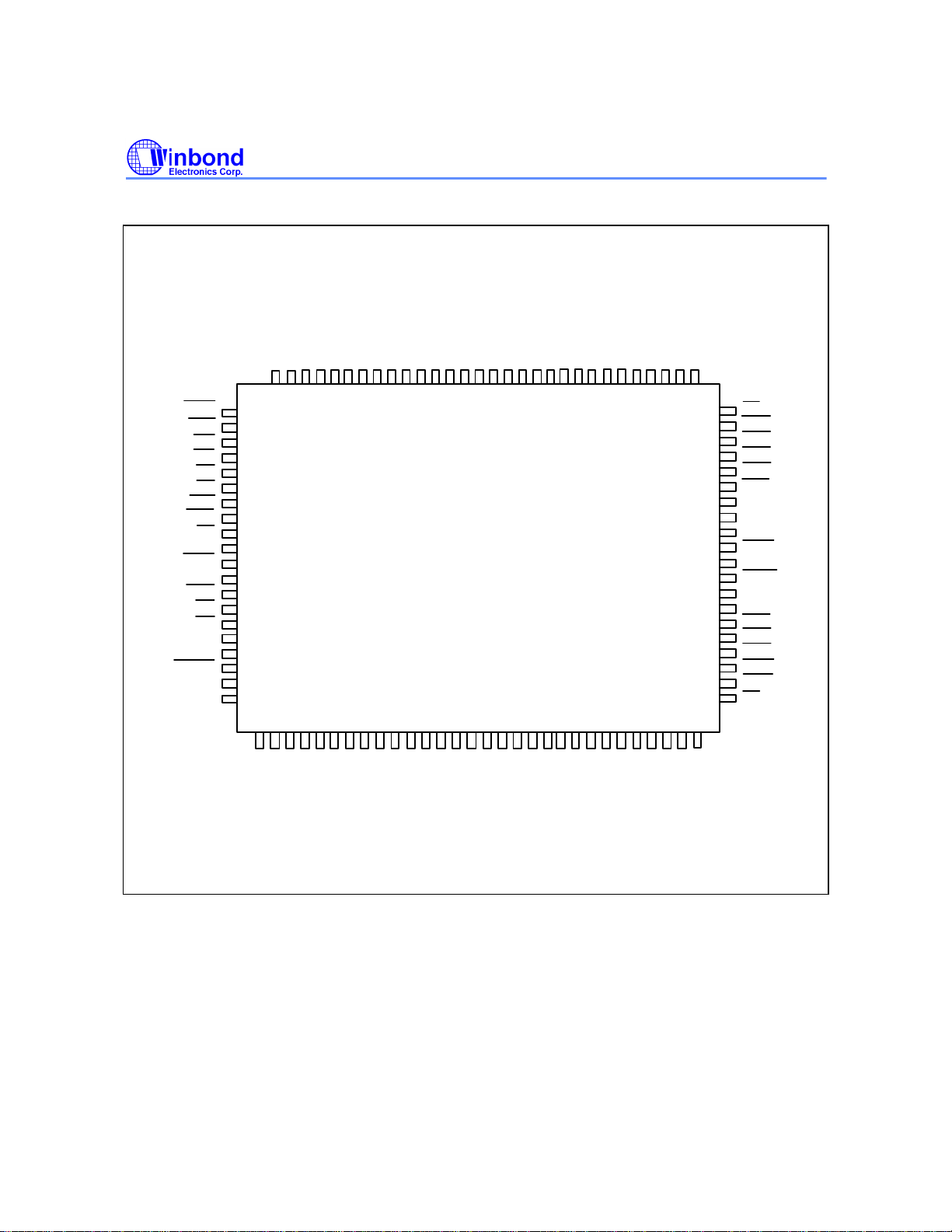
PIN CONFIGURATION
0
W
9
5
/
T
/
/
R
M
M
A
O
O
K
A
B
0
X X X X
80 79 78 77 76 75 74 73 72 71 70 69 68 67 66 65 64 63 62 61 60 59 58 57 56 55 54 53 52 51
DSA
DSB
WE
WD
DIR
GND
CS0
CS1
TC
X
81
X
82
X
83
X
84
X
85
X
86
X
87
X
88
X
89
X
90
X
91
X
92
X
93
X
94
X
95
X
96
X
97
X
98
X
99
X
100
1 2 3 4 5 6 7 8 9 10 11 1213 14 15 16 17 18 19 20 21 22 2324 2526 27 28 29 30
X X X X X
INDEX
STEP
RWC
HEAD
IDBEN
IRQ_B
IRQIN
IRQ_A
DACK_B
IRQ_F
DRQ_B
W83877F
/
D
/
S
R
K
D
A
N
C
A
1
W
H
T
P
G
A
D
D
D
4
3D2
X X X
D
1
D
D
5
6
7
X X X X
G
D
N
0
D
X X X X
X X X X
/
/
I
I
A
O
A
O
R
E
N
XX X X X X
XXX X X X X
A8A7A
X X X
X X X X X X X X XX
V
A
A
D
A2A
A
5
4
6
D
X
A
1
3
0
X
RIB
50
X
DCDB
49
X
DSRB
48
X
CTSB
47
X
46
DTRB
X
45
RTSB
X
44
IRQ_C
X
SOUTB
43
X
42
SINB
X
41
GMRD
X
40
GND
X
39
GMWR
X
38
SOUTA
X
IRQ_D
37
X
36
RTSA
X
35
DTRA
X
34
CTSA
X
33
DSRA
X
32
DCDA
X
31
RIA
X
P
P
P
/
/
/
/
P
D
/
I
M
P
R
D
R
C
O
E
S
S
I
D
E
RXT
C
Q
C
I
|
H
N
C
R
D
Y
D
T
D
1
A
A
0
L
L
2
1
P
P
P
V
P
D
D
D
D
4
2
3
/
D
D
D
D
6
D
7
A
C
K
|
C
/
S
T
B
I
S
A
I
R
L
F
N
Q
I
D
I
|
N
T
E
P
B
G
/
/
S
S
E
U
N
S
D
Y
E
A
L
I
R
C
C
N
R
K
T
A
- 4 -
1.0 PIN DESCRIPTION
CS
IOR
IOW
Note: Refer to section 9.2 DC CHARACTERISTICS for details.
I/O8t - TTL level bidirectional pin with 8 mA source-sink capability
I/O12t - TTL level bidirectional pin with 12 mA source-sink capability
I/O24t - TTL level bidirectional pin with 24 mA source-sink capability
OUT8t - TTL level output pin with 8 mA source-sink capability
OUT12t - TTL level output pin with 12 mA source-sink capability
OD12 - Open-drain output pin with 12 mA sink capability
OD24 - Open-drain output pin with 24 mA sink capability
INt - TTL level input pin
INc - CMOS level input pin
INcs - CMOS level schmitt-triggered input pin
1.1 Host Interface
SYMBOL PIN I/O FUNCTION
W83877F
D0−D7
A0−A9
66-73 I/O
51-55
IN
57-61
A10 75 IN
IOCHRDY 5 OD
MR 6 IN
2 IN
AEN 62 IN
63 IN
64 IN
DRQ_B 100 OUT
DACK_B
98 IN
DRQ_C 4 OUT
DACK_C
18 IN
TC 97 IN
System data bus bits 0-7
24t
System address bus bits 0-9
c
In ECP Mode, this pin is the A10 address input.
c
In EPP Mode, this pin is the IO Channel Ready output to extend
24
the host read/write cycle.
Master Reset. Active high. MR is low during normal operations.
cs
Active low chip select signal
t
System address bus enable
c
CPU I/O read signal
cs
CPU I/O write signal
cs
DMA request signal B
12t
DMA Acknowledge signal B
c
DMA request signal C
12t
DMA Acknowledge signal C
c
Terminal Count. When active, this pin indicates termination of a
c
DMA transfer.
IRQIN
93 IN
Interrupt request input
c
Publication Release Date: January 1996
- 5 - Revision A2
1.1 Host Interface, continued
CTSA
CTSB
DSRA
DSRB
DCDA
DCDB
RIA
RIB
SYMBOL PIN I/O FUNCTION
IRQ_A /
GIO1
96 OUT
I/O
When CR16 Bit 4 (GOIQSEL) = 0: Interrupt request signal A;
12t
When CR16 Bit 4 (GOIQSEL) = 1: General Purpose I/O port 1.
12t
W83877F
IRQ_B /
GIO0
92 OUT
I/O
IRQ_C 44 OUT
IRQ_D 37 OUT
IRQ_E 23 OUT
IRQ_F 99 OUT
XTAL1 7 IN
XTAL2 8 OUT
When CR16 Bit 4 (GOIQSEL) = 0: Interrupt request signal B;
12t
When CR16 Bit 4 (GOIQSEL) = 1: General Purpose I/O port 0.
12t
Interrupt request signal C
12t
Interrupt request signal D
12t
Interrupt request signal E
12t
Interrupt request signal F
12t
XTAL oscillator input
c
XTAL oscillator output
8t
1.2 Serial Port Interface
SYMBOL PIN I/O FUNCTION
34
47
33
48
32
49
IN
IN
IN
Clear To Send is the modem control input.
t
The function of these pins can be tested by reading Bit 4 of the
handshake status register.
Data Set Ready. An active low indicates the modem or data set
t
is ready to establish a communication link and transfer data to
the UART.
Data Carrier Detect. An active low indicates the modem or data
t
set has detected a data carrier.
SINA
SINB/IRRX1
SOUTA/
PIRIDE
31
IN
50
30
IN
42
38 I/O
Ring Indicator. An active low indicates that a ring signal is being
t
received by the modem or data set.
Serial Input. Used to receive serial data from the communication
t
link.
UART A Serial Output. Used to transmit serial data out to the
8t
communication link.
During power-on reset, this pin is pulled up internally and is
defined as PIRIDE, which provides the power-on value for CR16
bit 1 (IRIDE). A 47 kΩ is recommended when intends to pull
down at power-on reset.
- 6 -

1.2 Serial Port Interface, continued
DTRA
DTRB
RTSA
RTSB
SYMBOL PIN I/O FUNCTION
W83877F
SOUTB/
IRTX1/
PGMDRQ
PHEFRAS
PPNPCVS
PGOIQSEL
43 I/O
35 I/O
46 O
36 I/O
45 I/O
UART B Serial Output. Used to transmit serial data out to the
8t
communication link.
During power-on reset, this pin is pulled up internally and is
defined as PGMDRQ, which provides the power-on value for
CR16 bit 3 (GMDRQ). A 47 kΩ is recommended when intends
to pull down at power-on reset.
UART A Data Terminal Ready. An active low informs the
8t
modem or data set that the controller is ready to communicate.
During power-on reset, this pin is pulled down internally and is
defined as PHEFRAS, which provides the power-on value for
CR16 bit 0 (HEFRAS). A 47 kΩ is recommended when intends
to pull up at power-on reset.
UART B Data Terminal Ready. An active low informs the
8t
modem or data set that controller is ready to communicate.
UART A Request To Send. An active low informs the modem or
8t
data set that the controller is ready to send data.
During power-on reset, this pin is pulled up internally and is
defined as PPNPCVS, which provides the power-on value for
CR16 bit 2 (PNPCVS). A 47 kΩ is recommended when intends
to pull down at power-on reset.
UART B Request To Send. An active low informs the modem or
8t
data set that the controller is ready to send data.
During power-on reset, this pin is pulled down internally and is
defined as PGOIQSEL, which provides the power-on value for
CR16 bit 4 (GOIQSEL). A 47 kΩ is recommended when intends
to pull up at power-on reset.
Publication Release Date: January 1996
- 7 - Revision A2

W83877F
GMRD
GMWR
1.3 Game Port/Power Down Interface
If Bit 3 of CR16 (GMDRQ) is 1, Bit 4 of CR3 (GMODS0) determines whether the game port is in
Adapter mode or Portable mode (default is Adapter mode). If Bit 3 of CR16 is 0, pin 39 and 41 are
used for DMA A operation.
SYMBOL PIN I/O FUNCTION
41 OUT
PFDCEN
DACK_A
OUT
OUT
39 OUT
PEXTEN
DRQ_A
OUT
IN
PDCIN 3 IN
When CR16 Bit 3 (GMDRQ) = 1:
8t
Adapter mode: Game port read control signal.
8t
Portable mode: When parallel port is selected as Extension
FDD/Extension 2FDD mode, this pin will be active. The active
state is dependent on bit 7 of CRA (PFDCACT), and default is
low active.
8t
When CR16 Bit 3 (GMDRQ) = 0:
DMA acknowledge signal A.
When CR16 Bit 3 (GMDRQ) = 1:
8t
Adapter mode: Game port write control signal.
8t
Portable mode: When a particular extended mode is selected for
the parallel port, this pin will be active. The extended modes
include Extension Adapter mode, EPP mode, ECP mode, and
ECP/EPP mode, which are selected using bit 3 - bit 0 of CRA.
The active state is dependent on bit 6 of CRA (PEXTACT); the
default is low active.
When CR16 Bit 3 (GMDRQ) = 0:
t
DMA request signal A.
This input pin controls the chip power down. When this pin is
c
active, the clock supply to the chip will be inhibited and the
output pins will be tri-stated as defined in CR4 and CR6. The
PDCIN is pulled down internally. Its active state is defined by bit
4 of CRA (PDCHACT). Default is high active.
- 8 -
W83877F
MOB
2
MOB
MOB
2
MOB
ACK
ACK
DSB
2
DSB
DSB
2
DSB
1.4 Multi-Mode Parallel Port
The following pins have eight functions, which are controlled by bits PRTMOD0, PRTMOD1, and
PRTMOD2 of CR0 and CR9 (refer to section 8.0, Extended Functions).
SYMBOL PIN I/O FUNCTION
BUSY 24 IN
OD
IN
OD
26 IN
PRINTER MODE: BUSY
t
An active high input indicates that the printer is not ready to
receive data. This pin is pulled high internally. Refer to the
description of the parallel port for the definition of this pin in ECP
and EPP mode.
12
EXTENSION FDD MODE:
This pin is for Extension FDD B; the function of this pin is the
same as that of the
t
pin.
EXTENSION ADAPTER MODE: XIRQ
This pin is an interrupt request generated by the Extension
Adapter and is an active high input.
12
EXTENSION 2FDD MODE:
This pin is for Extension FDD A and B; the function of this pin is
_
the same as that of the
pin.
JOYSTICK MODE: NC pin.
t
PRINTER MODE:
An active low input on this pin indicates that the printer has
received data and is ready to accept more data. This pin is
pulled high internally. Refer to the description of the parallel port
for the definition of this pin in ECP and EPP mode.
OD
IN
OD
EXTENSION FDD MODE:
12
This pin is for the Extension FDD B; its functions are the same
as those of the
EXTENSION ADAPTER MODE: XDRQ
t
pin.
DMA request generated by the Extension Adapter. An active
high input.
EXTENSION 2FDD MODE:
12
This pin is for Extension FDD A and B; this function of this pin is
the same as that of the
_
JOYSTICK MODE: NC pin.
pin.
Publication Release Date: January 1996
- 9 - Revision A2
1.4 Multi-Mode Parallel Port, continued
WD
2
WD
2
WE
2
SYMBOL PIN I/O FUNCTION
PE 27 IN
PRINTER MODE: PE
t
An active high input on this pin indicates that the printer has
detected the end of the paper. This pin is pulled high internally.
Refer to the description of the parallel port for the definition of
this pin in ECP and EPP mode.
W83877F
OD
OUT
OD
SLCT 28 IN
OD
OUT
OD
EXTENSION FDD MODE:
12
This pin is for Extension FDD B; its function is the same as that
of the WD pin.
12t
EXTENSION ADAPTER MODE: XA0
This pin is system address A0 for the Extension Adapter.
12
EXTENSION 2FDD MODE:
This pin is for Extension FDD A and B; this function of this pin is
_
the same as that of the WD pin.
JOYSTICK MODE: NC pin.
PRINTER MODE: SLCT
t
An active high input on this pin indicates that the printer is
selected. This pin is pulled high internally. Refer to the
description of the parallel port for the definition of this pin in ECP
and EPP mode.
12
EXTENSION FDD MODE: WE2
This pin is for Extension FDD B; its functions are the same as
12t
those of the WE pin.
EXTENSION ADAPTER MODE: XA1
12
This pin is system address A1 for the Extension Adapter.
EXTENSION 2FDD MODE:
_
This pin is for Extension FDD A and B; this function of this pin is
the same as that of the WE pin.
JOYSTICK MODE: NC pin.
- 10 -
1.4 Multi-Mode Parallel Port, continued
ERR
ERR
HEAD
2
HEAD
HEAD
2
HEAD
SLIN
SLIN
STEP
2
STEP
STEP
2
STEP
SYMBOL PIN I/O FUNCTION
W83877F
29 IN
OD
OUT
OD
_
22 OD
OD
OUT
OD
OUT
t
PRINTER MODE:
An active low input on this pin indicates that the printer has
encountered an error condition. This pin is pulled high internally.
Refer to the description of the parallel port for the definition of
this pin in ECP and EPP mode.
EXTENSION FDD MODE:
12
This pin is for Extension FDD B; its function is the same as that
of the
EXTENSION ADAPTER MODE: XA2
12t
pin.
This pin is system address A2 for the Extension Adapter.
EXTENSION 2FDD MODE:
12
This pin is for Extension FDD A and B; its function is the same
as that of the
pin.
JOYSTICK MODE: NC pin.
12
PRINTER MODE:
Output line for detection of printer selection. This pin is pulled
high internally. Refer to the description of the parallel port for the
definition of this pin in ECP and EPP mode.
EXTENSION FDD MODE:
12
This pin is for Extension FDD B; its function is the same as that
12t
of the
pin.
EXTENSION ADAPTER MODE: XTC
This pin is the DMA terminal count for the Extension Adapter.
The count is sent by TC directly.
12
EXTENSION 2FDD MODE:
This pin is for Extension FDD A and B; its function is the same
12t
as that of the
pin .
JOYSTICK MODE: VDD for joystick.
Publication Release Date: January 1996
- 11 - Revision A2
1.4 Multi-Mode Parallel Port, continued
INIT
INIT
DIR
2
DIR
XDACK
PDACKX
DIR
2
DIR
AFD
AFD
RWC
2
RWC
XRD
XRD
XWR
RWC
2
RWC
SYMBOL PIN I/O FUNCTION
W83877F
21 OD
OD
OUT
OD
OUT
20 OD
OD
OUT
OD
OUT
12
PRINTER MODE:
Output line for the printer initialization. This pin is pulled high
internally. Refer to the description of the parallel port for the
definition of this pin in ECP and EPP mode.
EXTENSION FDD MODE:
12
This pin is for Extension FDD B; its function is the same as that
12t
of the
pin.
EXTENSION ADAPTER MODE:
This pin is the DMA acknowledge output for the Extension
Adapter; the output is sent directly from
12
.
EXTENSION 2FDD MODE:
This pin is for Extension FDD A and B; its function is the same
12t
as that of the
pin.
JOYSTICK MODE: VDD for joystick.
12
PRINTER MODE:
An active low output from this pin causes the printer to auto feed
a line after a line is printed. This pin is pulled high internally.
Refer to the description of the parallel port for the definition of
this pin in ECP and EPP mode.
EXTENSION FDD MODE:
12
This pin is for Extension FDD B; its function is the same as that
12t
of the
pin.
EXTENSION ADAPTER MODE:
This pin is the I/O read command for the Extension Adapter.
When the Extension Adapter base address is written to the
Extension Adapter address register,
and
simultaneously so that the command register on the Extension
Adapter can latch the same base address.
12
EXTENSION 2FDD MODE:
This pin is for Extension FDD A and B; its function is the same
12t
as that of the
pin.
JOYSTICK MODE: VDD for joystick.
go low
- 12 -
1.4 Multi-Mode Parallel Port, continued
STB
STB
XWR
XRD
XWR
INDEX
2
INDEX
INDEX
2
INDEX
SYMBOL PIN I/O FUNCTION
W83877F
19 OD
OUT
OUT
PD0 9 I/O
I/O
I/O
IN
IN
12
PRINTER MODE:
An active low output is used to latch the parallel data into the
printer. This pin is pulled high internally. Refer to the description
of the parallel port for the definition of this pin in ECP and EPP
-
mode.
EXTENSION FDD MODE:
12t
This pin is a tri-state output.
EXTENSION ADAPTER MODE:
This pin is the I/O write command for the Extension Adapter.
When the Extension Adapter base address is written to the
-
Extension Adapter address register,
simultaneously so that the command register on the Extension
Adapter can latch the same base address.
12t
and
go low
EXTENSION 2FDD MODE: This pin is a tri-state output.
JOYSTICK MODE: VDD for joystick.
PRINTER MODE: PD0
24t
Parallel port data bus bit 0. Refer to the description of the
parallel port for the definition of this pin in ECP and EPP mode.
EXTENSION FDD MODE:
t
This pin is for Extension FDD B; the function of this pin is the
same as that of the
EXTENSION ADAPTER MODE: XD0
24t
pin. This pin is pulled high internally.
This pin is system data bus D0 for the Extension Adapter.
t
EXTENSION 2FDD MODE:
This pin is for Extension FDD A and B; this function of this pin is
the same as
JOYSTICK MODE: JP0
24t
pin. This pin is pulled high internally.
This pin is the paddle 0 input for joystick.
Publication Release Date: January 1996
- 13 - Revision A2

1.4 Multi-Mode Parallel Port, continued
TRAK
02
TRAK
0
TRAK
02
TRAK
0
WP
2
WP
2
SYMBOL PIN I/O FUNCTION
W83877F
PD1 10 I/O
I/O
I/O
PD2 11 I/O
I/O
IN
IN
IN
IN
PRINTER MODE: PD1
24t
Parallel port data bus bit 1. Refer to the description of the
parallel port for the definition of this pin in ECP and EPP mode.
EXTENSION FDD MODE:
t
This pin is for Extension FDD B; the function of this pin is the
same as that of the
EXTENSION ADAPTER MODE: XD1
24t
pin. This pin is pulled high internally.
This pin is system data bus D1 for the Extension Adapter.
t
EXTENSION. 2FDD MODE:
This pin is for Extension FDD A and B; this function of this pin is
the same as
24t
JOYSTICK MODE: JP1
pin. This pin is pulled high internally.
This pin is the paddle 1 input for joystick.
PRINTER MODE: PD2
24t
Parallel port data bus bit 2. Refer to the description of the
parallel port for the definition of this pin in ECP and EPP mode.
EXTENSION FDD MODE:
t
This pin is for Extension FDD B; the function of this pin is the
same as that of the WP pin. This pin is pulled high internally.
EXTENSION ADAPTER MODE: XD2
24t
This pin is system data bus D2 for the Extension Adapter.
t
EXTENSION. 2FDD MODE:
This pin is for Extension FDD A and B; this function of this pin is
the same as that of the WP pin. This pin is pulled high
-
internally.
JOYSTICK MODE: NC pin
- 14 -
1.4 Multi-Mode Parallel Port, continued
RDATA
2
RDATA
RDATA
2
RDATA
DSKCHG
2
DSKCHG
DSKCHG
2
DSKCHG
SYMBOL PIN I/O FUNCTION
PD3 12 I/O
PRINTER MODE: PD3
24t
Parallel port data bus bit 3. Refer to the description of the
parallel port for the definition of this pin in ECP and EPP mode.
IN
t
EXTENSION FDD MODE:
Motor on B for Extension FDD B; the function of this pin is the
I/O
same as that of the
24t
EXTENSION ADAPTER MODE: XD3
pin. This pin is pulled high internally.
This pin is system data bus D3 for the Extension Adapter.
IN
t
EXTENSION 2FDD MODE:
This pin is for Extension FDD A and B; this function of this pin is
-
the same as that of the
internally.
JOYSTICK MODE: NC pin
PD4 13 I/O
PRINTER MODE: PD4
24t
Parallel port data bus bit 4. Refer to the description of the
parallel port for the definition of this pin in ECP and EPP mode.
IN
t
EXTENSION FDD MODE:
Drive select B for Extension FDD B; the function of this pin is the
I/O
same as that of
EXTENSION ADAPTER MODE: XD4
24t
pin. This pin is pulled high internally.
This pin is system data bus D4 for the Extension Adapter.
IN
t
EXTENSION 2FDD MODE:
This pin is for Extension FDD A and B; this function of this pin is
the same as that of the
t
internally.
IN
JOYSTICK MODE: JB0
This pin is the button 0 input for the joystick.
PD5 14 I/O
PRINTER MODE: PD5
24t
Parallel port data bus bit 5. Refer to the description of the
parallel port for the definition of this pin in ECP and EPP mode.
-
EXTENSION FDD MODE:
This pin is a tri-state output.
I/O
24t
EXTENSION ADAPTER MODE: XD5
This pin is system data bus D5 for the Extension Adapter
-
EXTENSION 2FDD MODE:
This pin is a tri-state output.
IN
t
JOYSTICK MODE: JB1
This pin is the button 1 input for the joystick.
W83877F
pin. This pin is pulled high
pin. This pin is pulled high
Publication Release Date: January 1996
- 15 - Revision A2

1.4 Multi-Mode Parallel Port, continued
MOA
2
MOA
DSA
2
DSA
SYMBOL PIN I/O FUNCTION
W83877F
PD6 16 I/O
I/O
OD
PD7 17 I/O
I/O
PRINTER MODE: PD6
24t
Parallel port data bus bit 6. Refer to the description of the
-
parallel port for the definition of this pin in ECP and EPP mode.
EXTENSION FDD MODE:
This pin is a tri-state output.
24t
EXTENSION ADAPTER MODE: XD6
This pin is system data bus D6 for the Extension Adapter
24
EXTENSION. 2FDD MODE:
This pin is for Extension FDD A; its function is the same as that
-
of the
pin.
JOYSTICK MODE: NC pin
PRINTER MODE: PD7
24t
Parallel port data bus bit 7. Refer to the description of the
parallel port for the definition of this pin in ECP and EPP mode.
-
EXTENSION FDD MODE:
This pin is a tri-state output.
EXTENSION ADAPTER MODE: XD7
24t
This pin is system data bus D7 for the Extension Adapter.
OD
EXTENSION 2FDD MODE:
24
This pin is for Extension FDD A; its function is the same as that
of the
-
JOYSTICK MODE: NC pin
pin.
- 16 -
1.5 IDE and FDC Interface
RESIDE
IDBEN
CS1
CS1
CS
0
CS
WE
DIR
HEAD
RWC
WD
STEP
INDEX
SYMBOL PIN I/O FUNCTION
IRQ_G
IRQ_H
/
IRTX2
/
IRRX2
/
1 OUT
OUT
/
91 OUT
OUT
95 OUT
OUT
94 OUT
IN
85 OD
89
When CR16 Bit 1 (IRIDE) = 0: Active low reset signal for IDE;
12t
When CR16 Bit 1 (IRIDE) = 1: Interrupt request signal G.
12t
When CR16 Bit 1 (IRIDE) = 0: Active low enable signal for IDE;
12t
When CR16 Bit 1 (IRIDE) = 1: Interrupt request signal H.
12t
When CR16 Bit 1 (IRIDE) = 0: This pin is used to select the IDE
12t
12t
controller.
CR22.
decodes the HDC addresses specified in
When CR16 Bit 1 (IRIDE) = 1: Function as a InfraRed
transmission data line.
When CR16 Bit 1 (IRIDE) = 0: This pin is used to select the IDE
12t
controller.
t
When CR16 Bit 1 (IRIDE) = 1: Function as a InfraRed receiving
decodes HDC addresses specified in CR21.
line.
Write enable. An open drain output.
24
Direction of the head step motor. An open drain output.
24
W83877F
88 OD
87 OD
86 OD
82 OD
81 IN
Logic 0 = inward motion
Head select. This open drain output determines which disk drive
24
head is active.
Logic 1 = side 0
Logic 0 = side 1
Reduced write current. This signal can be used on two-speed
24
disk drives to select the transfer rate. An open drain output.
Logic 0 = 250 Kb/s
Logic 1 = 500 Kb/s
When bit 5 of CR9 (EN3MODE) is set to high, the three-mode
FDD function is enabled, and the pin will have a different
definition. Refer to the EN3MODE bit in CR9.
Write data. This logic low open drain writes precompensation
24
serial data to the selected FDD. An open drain output.
Step output pulses. This active low open drain output produces a
24
pulse to move the head to another track.
This schmitt input from the disk drive is active low when the
cs
head is positioned over the beginning of a track marked by an
index hole. This input pin is pulled up internally by an
approximately 1K ohm resistor. The resistor can be disabled by
bit 4 of CR6 (FIPURDWN).
Publication Release Date: January 1996
- 17 - Revision A2
1.5 IDE and FDC Interface, continued
TRAK
0
WP
RDATA
DSKCHG
MOA
MOB
DSA
DSB
SYMBOL PIN I/O FUNCTION
W83877F
78 IN
77 IN
74 IN
76 IN
79 OD
80 OD
83 OD
84 OD
Track 0. This schmitt input from the disk drive is active low when
cs
the head is positioned over the outermost track. This input pin is
pulled up internally by an approximately 1K ohm resistor. The
resistor can be disabled by bit 4 of CR6 (FIPURDWN).
Write protected. This active low schmitt input from the disk drive
cs
indicates that the diskette is write-protected. This input pin is
pulled up internally by an approximately 1K ohm resistor. The
resistor can be disabled by bit 4 of CR6 (FIPURDWN).
The read data input signal from the FDD. This input pin is pulled
cs
up internally by an approximately 1K ohm resistor. The resistor
can be disabled by bit 4 of CR6 (FIPURDWN).
Diskette change. This signal is active low at power on and
cs
whenever the diskette is removed. This input pin is pulled up
internally by an approximately 1K ohm resistor. The resistor can
be disabled by bit 4 of CR6 (FIPURDWN).
Motor A On. When set to 0, this pin enables disk drive 0. This is
24
an open drain output.
Motor B On. When set to 0, this pin enables disk drive 1. This is
24
an open drain output.
Drive Select A. When set to 0, this pin enables disk drive A. This
24
is an open drain output.
Drive Select B. When set to 0, this pin enables disk drive B. This
24
is an open drain output.
VDD 15,
+5 power supply for the digital circuitry
56
GND 25,
Ground
40
65,
90
2.0 FDC FUNCTIONAL DESCRIPTION
2.1 W83877F FDC
The floppy disk controller of the W83877F integrates all of the logic required for floppy disk control.
The FDC implements a PC/AT or PS/2 solution. All programmable options default to compatible
values. The FIFO provides better system performance in multi-master systems. The digital data
separator supports up to 1 M bits/sec data rate.
The FDC includes the following blocks: AT interface, Precompensation, Data Rate Selection, Digital
Data Separator, FIFO, and FDC Core.
- 18 -

2.1.1 AT interface
WR
DACK
DACK
W83877F
The interface consists of the standard asynchronous signals: RD,
and a data bus. The address lines select between the configuration registers, the FIFO and
control/status registers. This interface can be switched between PC/AT, Model 30, or PS/2 normal
modes. The PS/2 register sets are a superset of the registers found in a PC/AT.
2.1.2 FIFO (Data)
The FIFO is 16 bytes in size and has programmable threshold values. All command parameter
information and disk data transfers go through the FIFO. Data transfers are governed by the RQM
and DIO bits in the Main Status Register.
The FIFO defaults to disabled mode after any form of reset. This maintains PC/AT hardware
compatibility. The default values can be changed through the CONFIGURE command. The
advantage of the FIFO is that it allows the system a larger DMA latency without causing disk errors.
The following tables give several examples of the delays with a FIFO. The data are based upon the
following formula:
THRESHOLD # × (1/DATA/RATE) *8 - 1.5 µS = DELAY
FIFO THRESHOLD MAXIMUM DELAY TO SERVICING AT 500K BPS
Data Rate
1 Byte
2 Byte
8 Byte
15 Byte
1 × 16 µS - 1.5 µS = 14.5 µS
2 × 16 µS - 1.5 µS = 30.5 µS
8 × 16 µS - 1.5 µS = 6.5 µS
15 × 16 µS - 1.5 µS = 238.5 µS
, A0-A3, IRQ, DMA control,
FIFO THRESHOLD MAXIMUM DELAY TO SERVICING AT 1M BPS
Data Rate
1 Byte
2 Byte
8 Byte
15 Byte
At the start of a command the FIFO is always disabled and command parameters must be sent based
upon the RQM and DIO bit settings in the main status register. When the FDC enters the command
execution phase, it clears the FIFO of any data to ensure that invalid data are not transferred.
An overrun and underrun will terminate the current command and the data transfer. Disk writes will
complete the current sector by generating a 00 pattern and valid CRC. Reads require the host to
remove the remaining data so that the result phase may be entered.
DMA transfers are enabled with the SPECIFY command and are initiated by the FDC by activating
the DRQ pin during a data transfer command. The FIFO is enabled directly by asserting
addresses need not be valid.
Note that if the DMA controller is programmed to function in verify mode a pseudo read is performed
by the FDC based only on
. This mode is only available when the FDC has been configured
1 × 8 µS - 1.5 µS = 6.5 µS
2 × 8 µS - 1.5 µS = 14.5 µS
8 × 8 µS - 1.5 µS = 62.5 µS
15 × 8 µS - 1.5 µS = 118.5 µS
and
Publication Release Date: January 1996
- 19 - Revision A2

W83877F
into byte mode (FIFO disabled) and is programmed to do a read. With the FIFO enabled the above
operation is performed by using the new VERIFY command. No DMA operation is needed.
2.1.3 Data Separator
The function of the data separator is to lock onto the incoming serial read data. When a lock is
achieved the serial front end logic of the chip is provided with a clock which is synchronized to the
read data. The synchronized clock, called the Data Window, is used to internally sample the serial
data portion of the bit cell, and the alternate state samples the clock portion. Serial to parallel
conversion logic separates the read data into clock and data bytes.
The Digital Data Separator (DDS) has three parts: control logic, error adjustment, and speed tracking.
The DDS circuit cycles once every 12 clock cycles ideally. Any data pulse input will be synchronized
and then adjusted by immediate error adjustment. The control logic will generate RDD and RWD for
every pulse input. During any cycle where no data pulse is present, the DDS cycles are based on
speed. A digital integrator is used to keep track of the speed changes in the input data stream.
2.1.4 Write Precompensation
The write precompensation logic is used to minimize bit shifts in the RDDATA stream from the disk
drive. Shifting of bits is a known phenomenon in magnetic media and is dependent on the disk media
and the floppy drive.
The FDC monitors the bit stream that is being sent to the drive. The data patterns that require
precompensation are well known. Depending upon the pattern, the bit is shifted either early or late
relative to the surrounding bits.
¡@
2.1.5 Perpendicular Recording Mode
The FDC is also capable of interfacing directly to perpendicular recording floppy drives. Perpendicular
recording differs from the traditional longitudinal method in that the magnetic bits are oriented
vertically. This scheme packs more data bits into the same area.
FDCs with perpendicular recording drives can read standard 3.5" floppy disks and can read and write
perpendicular media. Some manufacturers offer drives that can read and write standard and
perpendicular media in a perpendicular media drive.
A single command puts the FDC into perpendicular mode. All other commands operate as they
normally do. The perpendicular mode requires a 1 Mbps data rate for the FDC. At this data rate the
FIFO eases the host interface bottleneck due to the speed of data transfer to or from the disk.
2.1.6 FDC Core
The W83877F FDC is capable of performing twenty commands. Each command is initiated by a
multi-byte transfer from the microprocessor. The result can also be a multi-byte transfer back to the
microprocessor. Each command consists of three phases: command, execution, and result.
Command
The microprocessor issues all required information to the controller to perform a specific operation.
Execution
The controller performs the specified operation.
Result
After the operation is completed, status information and other housekeeping information is provided
to the microprocessor.
- 20 -

2.1.7 FDC Commands
Command Symbol Descriptions:
C: Cylinder number 0 - 256
D: Data Pattern
DIR: Step Direction
DIR = 0, step out
DIR = 1, step in
DS0: Disk Drive Select 0
DS1: Disk Drive Select 1
DTL: Data Length
EC: Enable Count
EOT: End of Track
EFIFO: Enable FIFO
EIS: Enable Implied Seek
EOT: End of track
FIFOTHR: FIFO Threshold
GAP: Gap length selection
GPL: Gap Length
H: Head number
HDS: Head number select
HLT: Head Load Time
HUT: Head Unload Time
LOCK: Lock EFIFO, FIFOTHR, PTRTRK bits prevent affected by software reset
MFM: MFM or FM Mode
MT: Multitrack
N: The number of data bytes written in a sector
NCN: New Cylinder Number
ND: Non-DMA Mode
OW: Overwritten
PCN: Present Cylinder Number
POLL: Polling Disable
PRETRK: Precompensation Start Track Number
R: Record
RCN: Relative Cylinder Number
R/W: Read/Write
SC: Sector/per cylinder
SK: Skip deleted data address mark
W83877F
Publication Release Date: January 1996
- 21 - Revision A2

W83877F
SRT: Step Rate Time
ST0: Status Register 0
ST1: Status Register 1
ST2: Status Register 2
ST3: Status Register 3
WG: Write gate alters timing of WE
(1) Read Data
PHASE R/W D7 D6 D5 D4 D3 D2 D1 D0 REMARKS
Command W MT MFM SK 0 0 1 1 0 Command codes
W 0 0 0 0 0 HDS DS1 DS0
W
W
W
W
W
W
W -------------------- DTL -----------------------
---------------------- C ------------------------
---------------------- H ------------------------
---------------------- R ------------------------
---------------------- N ------------------------
-------------------- EOT -----------------------
-------------------- GPL -----------------------
Sector ID information prior
to command execution
Execution Data transfer between the
FDD and system
Result R
R
R
R
R
R
R
-------------------- ST0 -----------------------
-------------------- ST1 -----------------------
-------------------- ST2 -----------------------
---------------------- C ------------------------
---------------------- H ------------------------
---------------------- R ------------------------
---------------------- N ------------------------
Status information after
command execution
Sector ID information after
command execution
- 22 -

W83877F
(2) Read Deleted Data
PHASE R/W D7 D6 D5 D4 D3 D2 D1 D0 REMARKS
Command W MT MFM SK 0 1 1 0 0 Command codes
W 0 0 0 0 0 HDS DS1 DS0
W
W
W
W
W
W
W -------------------- DTL -----------------------
Execution Data transfer between the
Result R
R
R
R
R
R
R
---------------------- C ------------------------
---------------------- H ------------------------
---------------------- R ------------------------
---------------------- N ------------------------
-------------------- EOT -----------------------
-------------------- GPL -----------------------
-------------------- ST0 -----------------------
-------------------- ST1 -----------------------
-------------------- ST2 -----------------------
---------------------- C ------------------------
---------------------- H ------------------------
---------------------- R ------------------------
---------------------- N ------------------------
Sector ID information prior
to command execution
FDD and system
Status information after
command execution
Sector ID information after
command execution
Publication Release Date: January 1996
- 23 - Revision A2

W83877F
(3) Read A Track
PHASE R/W D7 D6 D5 D4 D3 D2 D1 D0 REMARKS
Command W 0 MFM 0 0 0 0 1 0 Command codes
W 0 0 0 0 0 HDS DS1 DS0
W
W
W
W
W
W
W -------------------- DTL -----------------------
Execution Data transfer between the
Result R
R
R
R
R
R
---------------------- C ------------------------
---------------------- H ------------------------
---------------------- R ------------------------
---------------------- N ------------------------
-------------------- EOT -----------------------
-------------------- GPL -----------------------
-------------------- ST0 -----------------------
-------------------- ST1 -----------------------
-------------------- ST2 -----------------------
---------------------- C ------------------------
---------------------- H ------------------------
---------------------- R ------------------------
Sector ID information prior
to command execution
FDD and system; FDD
reads contents of all
cylinders from index hole to
EOT
Status information after
command execution
Sector ID information after
command execution
R
---------------------- N ------------------------
- 24 -

W83877F
(4) Read ID
PHASE R/W D7 D6 D5 D4 D3 D2 D1 D0 REMARKS
Command W 0 MFM 0 0 1 0 1 0 Command codes
W 0 0 0 0 0 HDS DS1 DS0
Execution The first correct ID
information on the cylinder
is stored in Data Register
Result R
R
R
R
R
R
R
(5) Verify
PHASE R/W D7 D6 D5 D4 D3 D2 D1 D0 REMARKS
Command W MT MFM SK 1 0 1 1 0 Command codes
W EC 0 0 0 0 HDS DS1 DS0
W
W
W
W
W
W
-------------------- ST0 -----------------------
-------------------- ST1 -----------------------
-------------------- ST2 -----------------------
---------------------- C ------------------------
---------------------- H ------------------------
---------------------- R ------------------------
---------------------- N ------------------------
---------------------- C ------------------------
---------------------- H ------------------------
---------------------- R ------------------------
---------------------- N ------------------------
-------------------- EOT -----------------------
-------------------- GPL -----------------------
-------------------- DTL/SC -------------------
Status information after
command execution
Disk status after the
command has been
completed
Sector ID information prior
to command execution
Execution No data transfer takes
place
Result R
R
R
R
R
R
R
-------------------- ST0 -----------------------
-------------------- ST1 -----------------------
-------------------- ST2 -----------------------
---------------------- C ------------------------
---------------------- H ------------------------
---------------------- R ------------------------
---------------------- N ------------------------
- 25 - Revision A2
Status information after
command execution
Sector ID information after
command execution
Publication Release Date: January 1996

W83877F
(6) Version
PHASE R/W D7 D6 D5 D4 D3 D2 D1 D0 REMARKS
Command W 0 0 0 1 0 0 0 0 Command code
Result R 1 0 0 1 0 0 0 0 Enhanced controller
(7) Write Data
PHASE R/W D7 D6 D5 D4 D3 D2 D1 D0 REMARKS
Command W MT MFM 0 0 0 1 0 1 Command codes
W 0 0 0 0 0 HDS DS1 DS0
W
W
W
W
W
W
W -------------------- DTL -----------------------
---------------------- C ------------------------
---------------------- H ------------------------
---------------------- R ------------------------
---------------------- N ------------------------
-------------------- EOT -----------------------
-------------------- GPL -----------------------
Sector ID information prior
to Command execution
Execution Data transfer between the
FDD and system
Result R
R
R
R
R
R
R
(8) Write Deleted Data
PHASE R/W D7 D6 D5 D4 D3 D2 D1 D0 REMARKS
Command W MT MFM 0 0 1 0 0 1 Command codes
W 0 0 0 0 0 HDS DS1 DS0
W
W
W
W
-------------------- ST0 -----------------------
-------------------- ST1 -----------------------
-------------------- ST2 -----------------------
---------------------- C ------------------------
---------------------- H ------------------------
---------------------- R ------------------------
---------------------- N ------------------------
---------------------- C ------------------------
---------------------- H ------------------------
---------------------- R ------------------------
---------------------- N ------------------------
Status information after
Command execution
Sector ID information after
Command execution
Sector ID information prior
to command execution
- 26 -

Write deleted data, continued
PHASE R/W D7 D6 D5 D4 D3 D2 D1 D0 REMARKS
W83877F
W
W
W
Execution Data transfer between the
Result R
R
R
R
R
R
R
(9) Format A Track
PHASE R/W D7 D6 D5 D4 D3 D2 D1 D0 REMARKS
Command W 0 MFM 0 0 1 1 0 1 Command codes
W 0 0 0 0 0 HDS DS1 DS0
W
W
W
W
-------------------- EOT -----------------------
-------------------- GPL -----------------------
-------------------- DTL -----------------------
-------------------- ST0 -----------------------
-------------------- ST1 -----------------------
-------------------- ST2 -----------------------
---------------------- C ------------------------
---------------------- H ------------------------
---------------------- R ------------------------
---------------------- N ------------------------
---------------------- N ------------------------
--------------------- SC -----------------------
--------------------- GPL ---------------------
---------------------- D ------------------------
FDD and system
Status information after
command execution
Sector ID information after
command execution
Bytes/Sector
Sectors/Cylinder
Gap 3
Filler Byte
Execution
for Each
Sector
Repeat:
Result R
W
W
W
W
---------------------- C ------------------------
---------------------- H ------------------------
---------------------- R ------------------------
---------------------- N ------------------------
-------------------- ST0 ----------------------R
R
R
R
R
R
-------------------- ST1 -----------------------
-------------------- ST2 -----------------------
---------------- Undefined -------------------
---------------- Undefined -------------------
---------------- Undefined -------------------
---------------- Undefined -------------------
Publication Release Date: January 1996
- 27 - Revision A2
Input Sector Parameters
Status information after
command execution

W83877F
(10) Recalibrate
PHASE R/W D7 D6 D5 D4 D3 D2 D1 D0 REMARKS
Command W 0 0 0 0 0 1 1 1 Command codes
W 0 0 0 0 0 0 DS1 DS0
Execution Head retracted to Track 0
Interrupt
(11) Sense Interrupt Status
PHASE R/W D7 76 D5 D4 D3 D2 D1 D0 REMARKS
Command W 0 0 0 0 1 0 0 0 Command code
Result R
R
(12) Specify
PHASE R/W D7 D6 D5 D4 D3 D2 D1 D0 REMARKS
Command W 0 0 0 0 0 0 1 1 Command codes
W
W
(13) Seek
PHASE R/W D7 D6 D5 D4 D3 D2 D1 D0 REMARKS
Command W 0 0 0 0 1 1 1 1 Command codes
W
W
Execution R Head positioned over proper
(14) Configure
---------------- ST0 -------------------------
---------------- PCN -------------------------
| ---------SRT ----------- | --------- HUT ---------- |
|------------ HLT ----------------------------------| ND
0 0 0 0 0 HDS DS1 DS0
-------------------- NCN -----------------------
Status information at the end
of each seek operation
cylinder on diskette
PHASE R/W D7 D6 D5 D4 D3 D2 D1 D0 REMARKS
Command W 0 0 0 1 0 0 1 1 Configure information
W
W
W
Execution Internal registers written
0 0 0 0 0 0 0 0
0 EIS EFIFO POLL | ------ FIFOTHR ----|
| --------------------PRETRK ---------------------- |
- 28 -
W83877F
(15) Relative Seek
PHASE R/W D7 D6 D5 D4 D3 D2 D1 D0 REMARKS
Command W 1 DIR 0 0 1 1 1 1 Command codes
W
W
(16) Dumpreg
PHASE R/W D7 D6 D5 D4 D3 D2 D1 D0 REMARKS
Command W 0 0 0 0 1 1 1 0 Registers placed in FIFO
Result R
R
R
R
R
R
R
R
R
R
0 0 0 0 0 HDS DS1 DS0
| -------------------- RCN ---------------------------- |
-------------------- PCN-Drive 0-----------------
-------------------- PCN-Drive 1 ----------------
-------------------- PCN-Drive 2-----------------
-------------------- PCN-Drive 3 ----------------
-------SRT ----------------- | --------- HUT --------
------------ HLT -------------------------------------| ND
-------------------- SC/EOT --------------------
LOCK 0 D3 D2 D1 D0 GAP WG
0 EIS EFIFO POLL | ------ FIFOTHR --------
--------------------PRETRK ---------------------
(17) Perpendicular Mode
PHASE R/W D7 D6 D5 D4 D3 D2 D1 D0 REMARKS
Command W 0 0 0 1 0 0 1 0 Command Code
W OW 0 D3 D2 D1 D0 GAP WG
(18) Lock
PHASE R/W D7 D6 D5 D4 D3 D2 D1 D0 REMARKS
Command W LOCK 0 0 1 0 1 0 0 Command Code
Result R 0 0 0 LOCK 0 0 0 0
(19) Sense Drive Status
PHASE R/W D7 D6 D5 D4 D3 D2 D1 D0 REMARKS
Command W 0 0 0 0 0 1 0 0 Command Code
W 0 0 0 0 0 HDS DS1 DS0
Result R ---------------- ST3 ------------------------- Status information about
disk drive
Publication Release Date: January 1996
- 29 - Revision A2
W83877F
DRV
2
(20) Invalid
PHASE R/W D7 D6 D5 D4 D3 D2 D1 D0 REMARKS
Command W ------------- Invalid Codes ----------------- Invalid codes (no operation
- FDC goes into standby
state)
Result R -------------------- ST0 ---------------------- ST0 = 80H
2.2 Register Descriptions
There are several status, data, and control registers in W83877F. These registers are defined below:
ADDRESS REGISTER
OFFSET READ WRITE
base address + 0
base address + 1
base address + 2
base address + 3
base address + 4 MS REGISTER DR REGISTER
base address + 5 DT (FIFO) REGISTER DT (FIFO) REGISTER
base address + 7 DI REGISTER CC REGISTER
SA REGISTER
SB REGISTER
TD REGISTER
DO REGISTER
TD REGISTER
2.2.1 Status Register A (SA Register) (Read base address + 0)
This register is used to monitor several disk interface pins in PS/2 and Model 30 modes. In PS/2
mode, the bit definitions for this register are as follows:
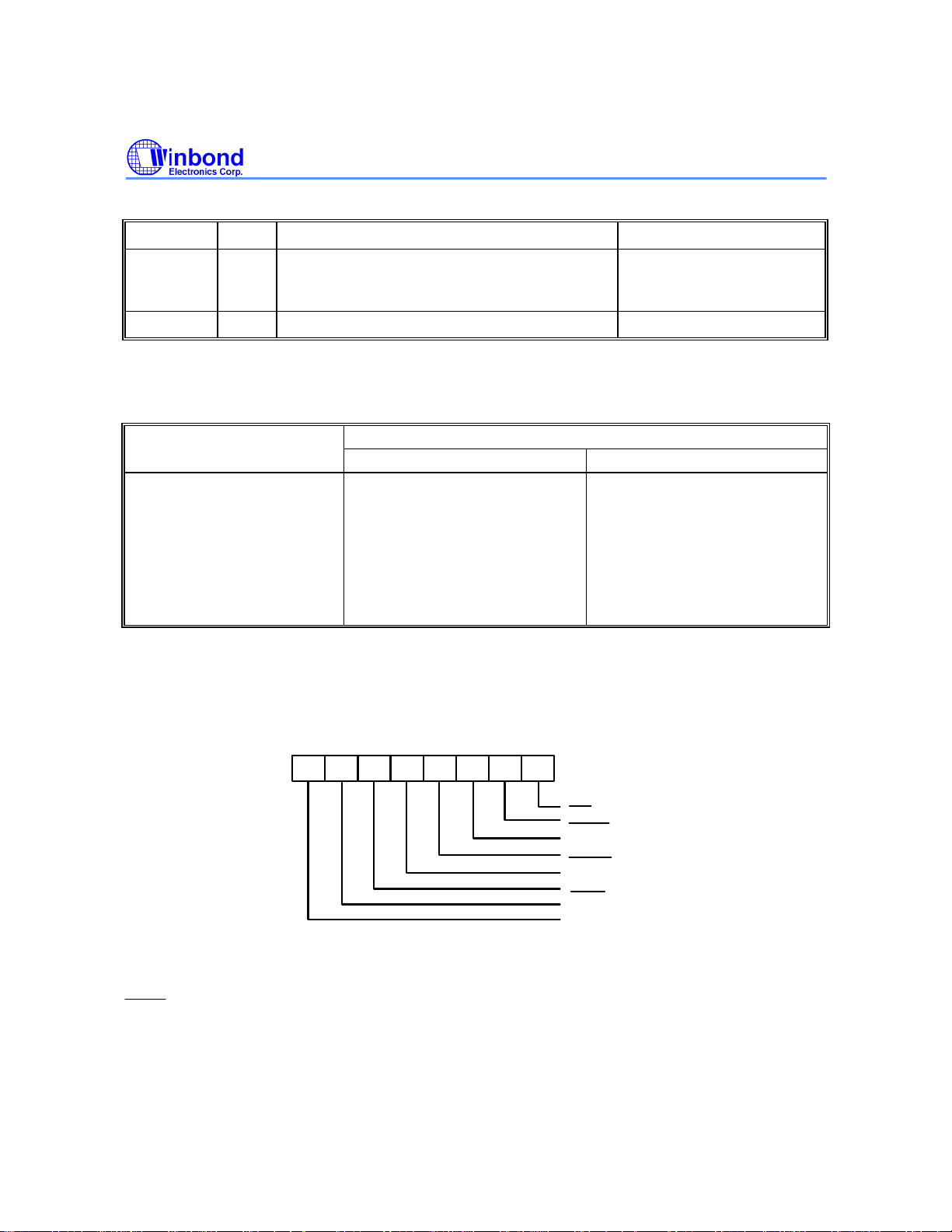
2
34567
1
0
DIR
WP
INDEX
HEAD
TRAK0
STEP
DRV2
INIT PENDING
INIT PENDING (Bit 7):
This bit indicates the value of the floppy disk interrupt output.
(Bit 6):
0 A second drive has been installed
1 A second drive has not been installed
- 30 -
 Loading...