

Winbond Electronics W83782D Datasheet

W83782D
Winbond H/W
Monitoring IC

W83782D Data Sheet Revision History
Pages Dates Version Version
1
2
3
4
5
6
7
8
9
10
n.a. n.a. All the version before 0.50 are for internal use.
n.a. 98/7 0.5 n.a. First publication.
P.40 99/4 0.55 A1 Add the content of Diode Selection Register Index
P.42 99/4 0.55 A1 Add the content of VBAT Monitor Control Register
Main Contents
on Web
59h(Bank0)
Index 5Dh (Bank0)
Please note that all data and specifications are subject to change without notice. All
the trade marks of products and companies mentioned in this data sheet belong to
their respective owners.
LIFE SUPPORT APPLICATIONS
These products are not designed for use in life support appliances, devices, or
systems where malfunction of these products can reasonably be expected to result
in personal injury. Winbond customers using or selling these products for use in
such applications do so at their own risk and agree to fully indemnify Winbond for
any damages resulting from such improper use or sales.

Preliminary W83782D
TABLE OF CONTENTS
1. GENERAL DESCRIPTION ............................................................................................1
2. FEATURES.......................................................................................................................2
2.1 MONITORING ITEMS .........................................................................................................................2
2.2 ACTIONS ENABLING .........................................................................................................................2
2.3 GENERAL ............................................................................................................................................ 2
2.4 PACKAGE............................................................................................................................................2
3. KEY SPECIFICATIONS.................................................................................................3
4. PIN CONFIGURATION..................................................................................................3
5. PIN DESCRIPTION.........................................................................................................4
6. FUNCTIONAL DESCRIPTION......................................................................................7
6.1 GENERAL DESCRIPTION ...................................................................................................................7
6.2 ACCESS INTERFACE ..........................................................................................................................7
6.2.1 ISA interface .................................................................................................................................7
6.2.2 I2C interface.................................................................................................................................. 9
6.2.3 The first serial bus access timing are shown as follow: ...................................................................9
6.2.4 The serial bus timing of the temperature 2 and 3 is shown as follow:...........................................11
6.3 ANALOG INPUTS.............................................................................................................................. 14
6.3.1 Monitor over 4.096V voltage:......................................................................................................15
6.3.2 Monitor negative voltage:............................................................................................................15
6.3.3 Monitor temperature from thermistor:..........................................................................................16
6.3.4 Monitor temperature from Pentium IITM thermal diode or bipolar transistor 2N3904 .................16
6.4 FAN SPEED COUNT AND FAN SPEED CONTROL.........................................................................17
6.4.1 Fan speed count........................................................................................................................... 17
6.4.2 Fan speed control......................................................................................................................... 19
Publication Release Date: April 1999
- I - Version A1

Preliminary W83782D
6.5 TEMPERATURE MEASUREMENT MACHINE................................................................................20
6.5.1 The W83782D temperature sensor 1 SMI# interrupt has two modes: ...........................................21
6.5.2 The W83782D temperature sensor 2 and sensor 3 SMI# interrupt has two modes and it is
programmed at CR[4Ch] bit 6.....................................................................................................22
6.5.3 The W83782D temperature sensor 2 and 3 Over-Temperature (OVT) has two modes, and they are
programmed at Bank1 and Bank2 CR[52h] bit1 . These two bits needs to be programmed the same
value. ...........................................................................................................................................23
7. REGISTERS AND RAM ............................................................................................... 24
7.1 ADDRESS REGISTER (PORT X5H) .................................................................................................. 24
7.2 DATA REGISTER (PORT X6H)......................................................................................................... 25
7.3 CONFIGURATION REGISTER ¾ INDEX 40H...................................................................................26
7.4 INTERRUPT STATUS REGISTER 1¾ INDEX 41H............................................................................ 26
7.5 INTERRUPT STATUS REGISTER 2 ¾ INDEX 42H........................................................................... 27
7.6 SMI# MASK REGISTER 1 ¾ INDEX 43H..........................................................................................28
7.7 SMI# MASK REGISTER 2 ¾ INDEX 44H..........................................................................................28
7.8 RESERVED REGISTER ¾ INDEX 45H..............................................................................................29
7.9 CHASSIS CLEAR REGISTER -- INDEX 46H .................................................................................... 29
7.10 VID/FAN DIVISOR REGISTER ¾ INDEX 47H................................................................................29
7.11 SERIAL BUS ADDRESS REGISTER ¾ INDEX 48H........................................................................30
7.12 VALUE RAM ¾ INDEX 20H- 3FH OR 60H - 7FH (AUTO-INCREMENT).......................................31
7.13 VOLTAGE ID (VID4) & DEVICE ID - 49H .....................................................................................33
7.14 TEMPERATURE 2 AND TEMPERATURE 3 SERIAL BUS ADDRESS REGISTER--INDEX 4AH .33
7.15 PIN CONTROL REGISTER - INDEX 4BH.......................................................................................34
7.16 IRQ#/OVT# PROPERTY SELECT - INDEX 4CH.............................................................................35
7.17 FAN IN/OUT AND BEEP/GPO# CONTROL REGISTER - INDEX 4DH..........................................36
7.18 REGISTER 50H ~ 5FH BANK SELECT - INDEX 4EH (NO AUTO INCREASE) ............................37
- II -

Preliminary W83782D
7.19 WINBOND VENDOR ID - INDEX 4FH (NO AUTO INCREASE)....................................................37
7.20 WINBOND TEST REGISTER -- INDEX 50H - 55H (BANK 0).......................................................38
7.21 BEEP CONTROL REGISTER 1-- INDEX 56H (BANK 0)................................................................38
7.22 BEEP CONTROL REGISTER 2-- INDEX 57H (BANK 0)................................................................39
7.23 CHIP ID -- INDEX 58H (BANK 0)....................................................................................................40
7.24 DIODE SELECTION REGISTER -- INDEX 59H (BANK 0)............................................................ 40
7.25 PWMOUT2 CONTROL -- INDEX 5AH (BANK 0)....................................................................... 40-A
7.26 PWMOUT1 CONTROL -- INDEX 5BH (BANK 0) ...........................................................................41
7.27 PWMOUT1/2 CLOCK SELECT -- INDEX 5CH (BANK 0)..............................................................41
7.28 VBAT MONITOR CONTROL REGISTER -- INDEX 5DH (BANK 0).............................................. 42
7.29 PWMOUT3 CONTROL -- INDEX 5EH (BANK 0) ........................................................................... 43
7.30 PWMOUT4 CONTROL -- INDEX 5FH (BANK 0)............................................................................ 43
7.31 TEMPERATURE SENSOR 2 TEMPERATURE (HIGH BYTE) REGISTER - INDEX 50H (BANK1)44
7.32 TEMPERATURE SENSOR 2 TEMPERATURE (LOW BYTE) REGISTER - INDEX 51H (BANK1)44
7.33 TEMPERATURE SENSOR 2 CONFIGURATION REGISTER - INDEX 52H (BANK1)...................45
7.34 TEMPERATURE SENSOR 2 HYSTERESIS (HIGH BYTE) REGISTER - INDEX 53H (BANK 1) .. 46
7.35 TEMPERATURE SENSOR 2 HYSTERESIS (LOW BYTE) REGISTER - INDEX 54H (BANK 1)...46
7.36 TEMPERATURE SENSOR 2 OVER-TEMPERATURE (HIGH BYTE) REGISTER - INDEX 55H
(BANK 1) ............................................................................................................................................47
7.37 TEMPERATURE SENSOR 2 OVER-TEMPERATURE (LOW BYTE) REGISTER - INDEX 56H
(BANK 1) ............................................................................................................................................47
7.38 TEMPERATURE SENSOR 3 TEMPERATURE (HIGH BYTE) REGISTER - INDEX 50H (BANK2)48
7.39 TEMPERATURE SENSOR 3 TEMPERATURE (LOW BYTE) REGISTER - INDEX 51H (BANK2)48
7.40 TEMPERATURE SENSOR 3 CONFIGURATION REGISTER - INDEX 52H (BANK 2)..................48
7.41 TEMPERATURE SENSOR 3 HYSTERESIS (HIGH BYTE) REGISTER - INDEX 53H (BANK 2) .. 49
7.42 TEMPERATURE SENSOR 3 HYSTERESIS (LOW BYTE) REGISTER - INDEX 54H (BANK 2)...49
7.43 TEMPERATURE SENSOR 3 OVER-TEMPERATURE (HIGH BYTE) REGISTER - INDEX 55H
(BANK 2) ............................................................................................................................................50
7.44 TEMPERATURE SENSOR 3 OVER-TEMPERATURE (LOW BYTE) REGISTER - INDEX 56H
(BANK 2) ............................................................................................................................................50
7.45 INTERRUPT STATUS REGISTER 3¾ INDEX 50H (BANK4).......................................................... 51
7.46 SMI# MASK REGISTER 3 ¾ INDEX 51H (BANK 4).......................................................................51
7.47 BEEP CONTROL REGISTER 3-- INDEX 53H (BANK 4)................................................................52
7.48 RESERVED REGISTER - INDEX 54H--58H (BANK 4)...................................................................52
Publication Release Date: April 1999
- III - Version A1

Preliminary W83782D
7.49 REAL TIME HARDWARE STATUS REGISTER I -- INDEX 59H (BANK 4) ..................................53
7.50 REAL TIME HARDWARE STATUS REGISTER II -- INDEX 5AH (BANK 4)................................54
7.51 REAL TIME HARDWARE STATUS REGISTER III -- INDEX 5BH (BANK 4)...............................54
7.52 PWMOUT3/4 CLOCK SELECT -- INDEX 5CH (BANK 4)..............................................................55
7.53 VALUE RAM 2¾ INDEX 50H - INDEX 5AH (AUTO-INCREMENT) (BANK 5)............................ 56
7.54 WINBOND TEST REGISTER - INDEX 50H (BANK 6)...................................................................56
8. SPECIFICATIONS ........................................................................................................ 57
8.1 ABSOLUTE MAXIMUM RATINGS................................................................................................... 57
8.2 DC CHARACTERISTICS ................................................................................................................... 57
8.3 AC Characteristics...............................................................................................................................59
8.3.1 ISA Read/Write Interface Timing................................................................................................59
8.3.2 Serial Bus Timing Diagram......................................................................................................... 60
9. HOW TO READ THE TOP MARKING......................................................................61
10. PACKAGE DIMENTIONS..........................................................................................62
11. APPLICATION CIRCUIT OF WINBOND W83782D / 781D ...................................63
- IV -

Priliminary W83782D
WINBOND H/W MONITORING IC
1. GENERAL DESCRIPTION
W83782D is an evolving version of W83782D --- Winbond's most popular hardware status
monitoring IC. The W83782D can be used to monitor several critical hardware parameters of the
system, including power supply voltages, fan speeds, and temperatures, which are very important for
a high-end computer system to work stable and properly. W83782D provides both ISA and I2C
serial bus interface.
An 8-bit analog-to-digital converter (ADC) was built inside W83782D. The W83782D can
simultaneously monitor 9 analog voltage inputs, 2 fan tachometer inputs, 3 remote temperature, one
case-open detection signal. The remote temperature sensing can be performed by thermistors, or
2N3904 NPN-type transistors, or directly from IntelTM Deschutes CPU thermal diode output. Also the
W83782D provides: 4 PWM (pulse width modulation) outputs for the fan speed control; beep tone
output for warning; SMI#, OVT#, GPO# signals for system protection events.
Through the application software or BIOS, the users can read all the monitored parameters of system
from time to time. And a pop-up warning can be also activated when the monitored item was out of
the proper/preset range. The application software could be Winbond's Hardware DoctorTM, or Intel
LDCM (LanDesk Client Management), or other management application software. Also the users can
set up the upper and lower limits (alarm thresholds) of these monitored parameters and to activate
one programmable and maskable interrupts. An optional beep tone could be used as warning signal
when the monitored parameters is out of the preset range.
TM
TM
Additionally, 5 VID inputs are provided to read the VID of CPU (i.e. PentiumTM II) if applicable. This is
to provide the Vcore voltage correction automatically. Also W83782D uniquely provides an optional
feature: early stage (before BIOS was loaded) beep warning. This is to detect if the fatal elements
present --- Vcore or +3.3V voltage fail, and the system can not be boomed up. Also there are 3
specific pins to provide selectable address setting for application of multiple devices (up to 8 devices)
wired through I2CTM interface.
Publication Release Date: April 1999
- 1 - Revision A1

Preliminary W83782D
2. FEATURES
2.1 Monitoring Items
• 3 thermal inputs from remote thermistors or 2N3904 NPN-type transistors or PentiumTM II
(Deschutes) thermal diode output
• 9 voltage inputs
--- typical for Vcore, +3.3V, +12V, -12V, +5V, -5V, +5V Vsb, Vbat, and one reserved
• 3 fan speed monitoring inputs
• Case open detection input
• WATCHDOG comparison of all monitored values
• Programmable hysteresis and setting points (alarm thresholds) for all monitored items
2.2 Actions Enabling
• Beep tone warning
•
4 PWM (pulse width modulation) outputs for fan speed control (3 are MUX optional)
--- Total up to 3 sets of fan speed monitoring and controlling
• Issue SMI#, OVT#, GPO# signals to activate system protection
• Warning signal pop-up in application software
2.3 General
• ISA and I2CTM serial bus interface
• 5 VID input pins for CUP Vcore identification (for PentiumTM II)
• Initial power fault beep (for +3.3V, Vcore)
• Master reset input to W83782D
• Independent power plane of digital Vcc and analog Vcc (inputs to IC)
• 3 pins (IA0, IA1, IA2) to provide selectable address setting for application of multiple devices (up
to 8 devices) wired through I2CTM interface
• IntelTM LDCM (DMI driver 2.0) support
• AcerTM ADM (DMI driver 2.0) support
• Winbond hardware monitoring application software (Hardware Doctor
Windows 95/98 and Windows NT 4.0/5.0
• Input clock rate optional for 24, 48, 14.318 Mhz
• 5V Vcc operation
TM
) support, for both
2.4 Package
• 48-pin LQFP
- 2 -
Preliminary W83782D
3
#
3. KEY SPECIFICATIONS
• Voltage monitoring accuracy ±1% (Max)
• Monitoring Temperature Range and Accuracy
- 40°C to +120°C ± 3°C(Max)
• Supply Voltage 5V
• Operating Supply Current 5 mA typ.
• ADC Resolution 8 Bits
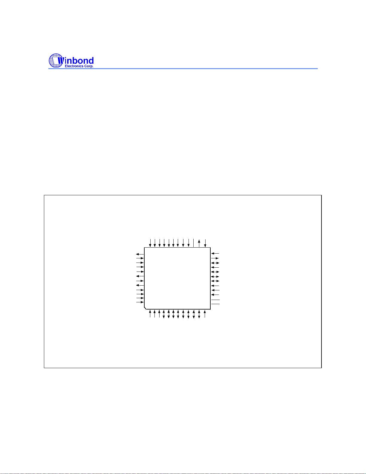
4. PIN CONFIGURATION
B
E
E
P
-
/
5
5
V
S
B
V
G
G
V
I
N
P
I
D
D
O
N
3
A
#
25
24
VID2
PWMTOUT1
SDA
C
S
FAN1IO
FAN2IO
FAN3IO/PWMOUT2
VID4
CASEOPEN
MR
G N D D
13
CC
V
12
VREF
VTIN3/PIITD3
VTIN2/PIITD2
VTIN1/PIITD1
VID0
OVT#
ARDMSEL
SMI#
SA2/IA2
SA1/IA1
SA0/IA0
CS#
V
V
+
C
I
3.3
O
V
R
N
I
E
R
N
A
0
36
37
48
1
+
+
-
12
5
V
12
V
V
B
V
I
I
A
I
N
N
T
N
W83782D
L
I
I
C
O
O
L
W
R
K
#
I
N
D
D
D
D
D6D
4
5
7
V
D
D
2
I
1
0
D
/
/
1
P
P
W
W
M
M
O
O
U
U
T
T
4
3
Publication Release Date: April 1999
- 3 - Revision A1
Preliminary W83782D
Bi-directional ISA bus Data lines. This pin is activated if pin
ADRMSEL=0. /
Fan speed control PWM output. This pin is activated if pin
ADRMSEL=1.
Bi-directional ISA bus Data lines. This pin is activated if pin
ADRMSEL=0. /
Fan speed control PWM output. This pin is activated if pin
ADRMSEL=1.
5. PIN DESCRIPTION
I/O
- TTL level bi-directional pin with 12 mA source-sink capability
12t
I/O
- TTL level and schmitt trigger
12ts
OUT12 - Output pin with 12 mA source-sink capability
AOUT - Output pin(Analog)
OD12 - Open-drain output pin with 12 mA sink capability
INt - TTL level input pin
INts - TTL level input pin and schmitt trigger
AIN - Input pin(Analog)
PIN NAME PIN NO. TYPE DESCRIPTION
IOR# 1 IN
IOW# 2 IN
CLKIN 3 IN
D7~D2 4-9 I/O
D1 /
10 I/O
ts
ts
t
12t
12t
An active low standard ISA bus I/O Read Control.
An active low standard ISA bus I/O Write Control.
System clock input. Can select 48MHz or 24MHz or 14.318MHz.
The default is 24MHz.
Bi-directional ISA bus Data lines. D0 corresponds to the low
order bit, with D7 the high order bit. These pins are activated if
pin ADRMSEL=0.
PWMOUT4
D0 /
11 I/O
PWMOUT3
VID1 12 IN
OUT
OUT
12t
12
12
t
Voltage Supply readouts from P6. This value is read in the
VID/Fan Divisor Register.
VCC (+5V) 13 POWER
+5V VCC power. Bypass with the parallel combination of 10µF
(electrolytic or tantalum) and 0.1µF (ceramic) bypass capacitors.
GNDD 14 DGROUND Internally connected to all digital circuitry.
MR 15 IN
CASEOPEN# 16 IN
ts
t
Master reset input.
CASE OPEN detection . An active low input from an external
device when case is opened. This signal can be latched if pin
VBAT is connect to battery, even W83782D is power off.
VID4 17 IN
t
Voltage Supply readouts from P6. This value is read in the bit
<0> of Device ID Register.
- 4 -
Preliminary W83782D
Pin Discription, continued
PIN NAME PIN NO. TYPE DESCRIPTION
FAN3IO/
PWMOUT2
FAN2IO-
FAN1IO
SCL 21 IN
SDA 22 OD
PWMOUT1 23 OUT
VID2 24 IN
VID3 25 IN
BEEP/GPO# 26 OD
GNDA 27 AGROUND Internally connected to all analog circuitry. The ground reference
-5VIN 28 AIN 0V to 4.096V FSR Analog Inputs.
5VSB 29 AIN 0V to 4.096V FSR Analog Inputs.
VBAT 30 AIN 0V to 4.096V FSR Analog Inputs. (This pin should be connected
-12VIN 31 AIN 0V to 4.096V FSR Analog Inputs.
+12VIN 32 AIN 0V to 4.096V FSR Analog Inputs.
+5VIN 33 AIN This pin is Analog Vcc and connects internal monitor channel
+3.3VIN 34 AIN 0V to 4.096V FSR Analog Inputs.
VINR0 35 AIN 0V to 4.096V FSR Analog Inputs.
VCOREA 36 AIN 0V to 4.096V FSR Analog Inputs.
VREF 37 AOUT Reference Voltage.
VTIN3 /
PIITD3
18 I/O
12t
0V to +5V amplitude fan tachometer input. /
Fan speed control PWM output.
19-20 I/O
12t
0V to +5V amplitude fan tachometer input /
Fan on-off control output. These multi-functional pins can be
programmable input or output.
ts
12
12
t
Serial Bus Clock.
Serial Bus bi-directional Data.
Fan speed control PWM output.
Voltage Supply readouts from P6. This value is read in the
VID/Fan Divisor Register.
t
Voltage Supply readouts from P6. This value is read in the
VID/Fan Divisor Register.
12
Beep (Default) / General purpose output
This multi-functional pin is programmable.
for all analog inputs.
to 3V BATTERY.)
IN3 with fixed scale.
38 AIN Thermistor 3 terminal input.(Default) /
PentiumTM II diode 3 input.
This multi-functional pin is programmable.
Publication Release Date: April 1999
- 5 - Revision A1

Preliminary W83782D
Pin Discription, continued
PIN NAME PIN NO. TYPE DESCRIPTION
VTIN2 /
PIITD2
VTIN1 /
PIITD1
VID0 41 IN
OVT# 42 OD
ADRMSEL 43 IN
SMI# 44 OD
SA2-SA0
IA2,IA1,IA0
CS# 48 IN
39 AIN Thermistor 2 terminal input. (Default)/
PentiumTM II diode 2 input.
This multi-functional pin is programmable.
40 AIN Thermistor 1 terminal input. (Default)/
PentiumTM II diode 1 input.
This multi-functional pin is programmable.
t
Voltage Supply readouts from P6. This value is read in the
VID/Fan Divisor Register.
12
t
Over temperature Shutdown Output.
Pin 45--47 mode selection.
0 = The 3 lowest order bits of ISA Address Bus.(Default, internal
pull-down 47K ohm)
1 = 7 bit I2CTM address setting pin.(bit2 - bit0)
12
System Management Interrupt (open drain). This output is
enabled when Bit 1 in the Configuration Register is set to 1. The
default state is disabled.
45-47 IN
t
The three lowest order bits of the 16-bit ISA Address Bus. A0
corresponds to the lowest order bit.
(Default, when ARDMSEL =0 or left open )
IN
t
t
The hardware setting pin of 7 bit I2CTM serial address bit2, bit1
and bit0 at CR[48h]. (When ARDMSEL =1)
Chip Select input from an external decoder which decodes high
order address bits on the ISA Address Bus. This is an active low
input.
- 6 -

Preliminary W83782D
6. FUNCTIONAL DESCRIPTION
6.1 General Description
The W83782D provides 7 analog positive inputs, 3 fan speed monitors, at most 4 sets for fan PWM
(Pulse Width Modulation) control, 3 thermal inputs from remote thermistors or 2N3904 transistors or
Pentium
the monitor value exceed the set limit value including voltage, temperature, or fan counter. When
start the monitor function on the chip, the watch dog machine monitor every function and store the
value to registers. If the monitor value exceeds the limit value, the interrupt status will be set to 1.
6.2 Access Interface
The W83782D provides two interface for microprocessor to read/write internal registers.
6.2.1 ISA interface
The first interface uses ISA Bus to access which the ports of low byte (bit2~bit0) are defined in the
port 5h and 6h. The high byte (from ISA address bus bit15~bit3) of these ports is decoded by Chip
Select (CS#), the general decoded address is set to port 295h and port 296h. These two ports are
described as following:
Port 295h: W83782D Index register port.
Port 296h: Data port.
The register structure is showed as the Figure 1.
TM
II (Deschutes) thermal diode outputs, case open detection and beep function output when
Publication Release Date: April 1999
- 7 - Revision A1
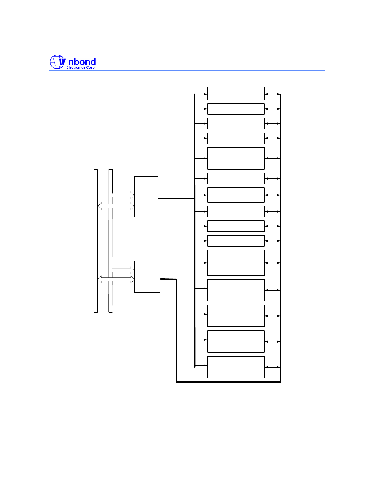
ISA
Data
Bus
ISA
Address
Bus
Port 5h
Index
Register
Port 6h
Data
Register
Preliminary W83782D
Configuration Register
40h
SMI# Status/Mask Registers
41h, 42h, 44h, 45h
VID<3:0>/Fan Divisor Register
Temperature 2, 3 Serial
Bus Address
Select Bank for 50h~5Fh Reg.
Temperature 2 Control/Staus
Registers
47h
Serial Bus Address
48h
Monitor Value Registers
20h~3Fh
and
60h~7Fh (auto-increment)
VID<4>/Device ID
49h
4Ah
Control Register
4Bh~4Dh
4Eh
Winbond Vendor ID
4Fh
BANK 0
R-T Table Value
BEEP Control Register
Winbond Test Register
50h~58h
BANK 1
50h~56h
Figure 1. ISA interface access diagram
- 8 -
BANK 2
Temperature 3 Control/Staus
Registers
50h~56h
BANK 4
Additional Control/Staus
Registers
50h~5Ch
BANK 5
Additional Limit Value &
Value RAM
50h~57h
Preliminary W83782D
6.2.2 I2C interface
The second interface uses I2C Serial Bus. In the W83782D has three serial bus address. That is, the
first address defined at CR[48h] can read/write all registers excluding Bank 1 and Bank 2 temperature
sensor 2/3 registers. The second address defined at CR[4Ah] bit2-0 only read/write temperature
sensor 2 registers, and the third address defined at CR[4Ah] bit6-4 only can access (read/write)
temperature sensor 3 registers.
The first serial bus address of W83782D has 3 hardware setting bits set by pin47-45 when pin 43 is
set to high. The address is 00101[pin45][pin46][pin47]. If pin45=1, pin46=1, pin47=0, for example, the
content of CR[48h] is 00101110. If CR[4Ah] bit 2-0 is XXX , the temperature sensor 2 serial address is
1001XXXG, in which G is the read/write bit. If CR[4Ah] bit 6-4 is YYY , the temperature sensor 3
serial address is 1001YYYG, in which G is the read/write bit.
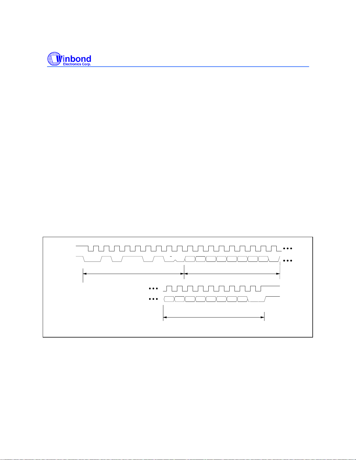
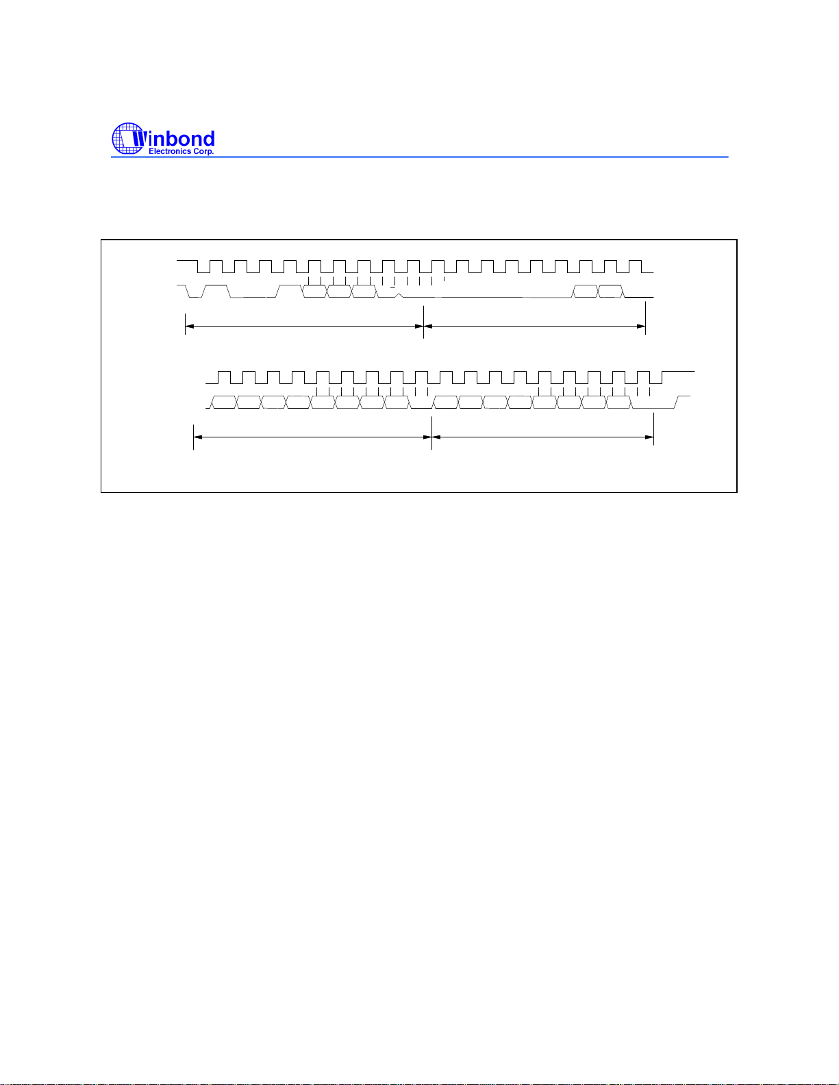
6.2.3 The first serial bus access timing are shown as follow:
(a) Serial bus write to internal address register followed by the data byte
SCL
SDA
0
0 1 0 1 1 0 1 D7 D6 D5 D4 D3 D2 D1 D0
Start By
Master
Figure 2. Serial Bus Write to Internal Address Register followed by the Data Byte
Frame 1
Serial Bus Address Byte
SCL
(Continued)
SDA (Continued)
7 8 0 7 8
R/W
Ack
by
781D
0
D7 D6 D5 D4 D3 D2 D1 D0
Frame 2
Internal Index Register Byte
Frame 3
Data Byte
7 8
Ack
by
781D
Stop
by
Master
Ack
by
781D
Publication Release Date: April 1999
- 9 - Revision A1
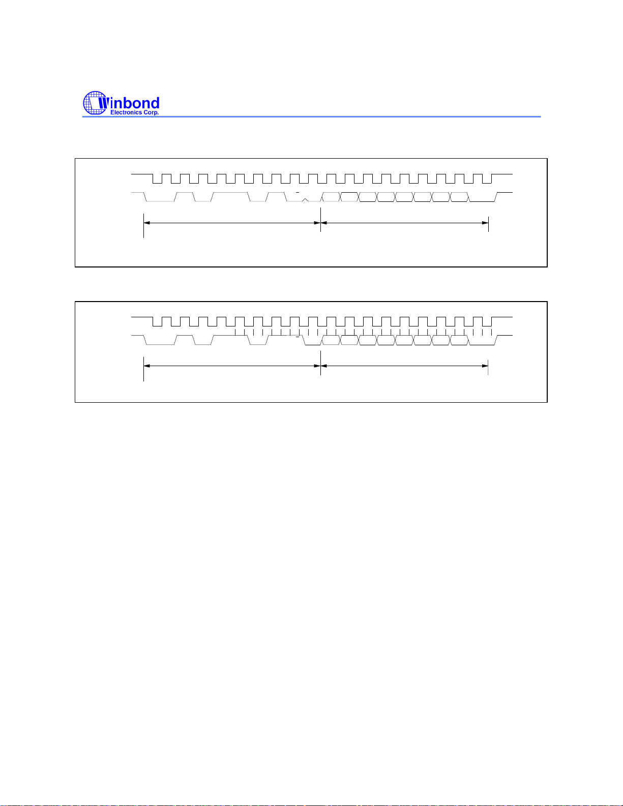
(b) Serial bus write to internal address register only
Preliminary W83782D
0
7 8 0 7 8
SCL
SDA
0 1 0 1 1 0 1 D7 D6 D5 D4 D3 D2 D1 D0
Start By
Master
Frame 1
Serial Bus Address Byte
R/W
Ack
781D
Ack
Stop by
by
by
Frame 2
Internal Index Register Byte
781D
Master
0
Figure 3. Serial Bus Write to Internal Address Register Only
(c) Serial bus read from a register with the internal address register prefer to desired location
SCL
SDA
0
0 1 0 1 1 0 1 D7 D6 D5 D4 D3 D2 D1 D0
Start By
Master
Frame 1
Serial Bus Address Byte
Figure 4. Serial Bus Write to Internal Address Register Only
7 8 0 7 8
R/W
Ack
781D
by
Frame 2
Internal Index Register Byte
0
Ack
by
Master
Stop by
Master
- 10 -
Preliminary W83782D
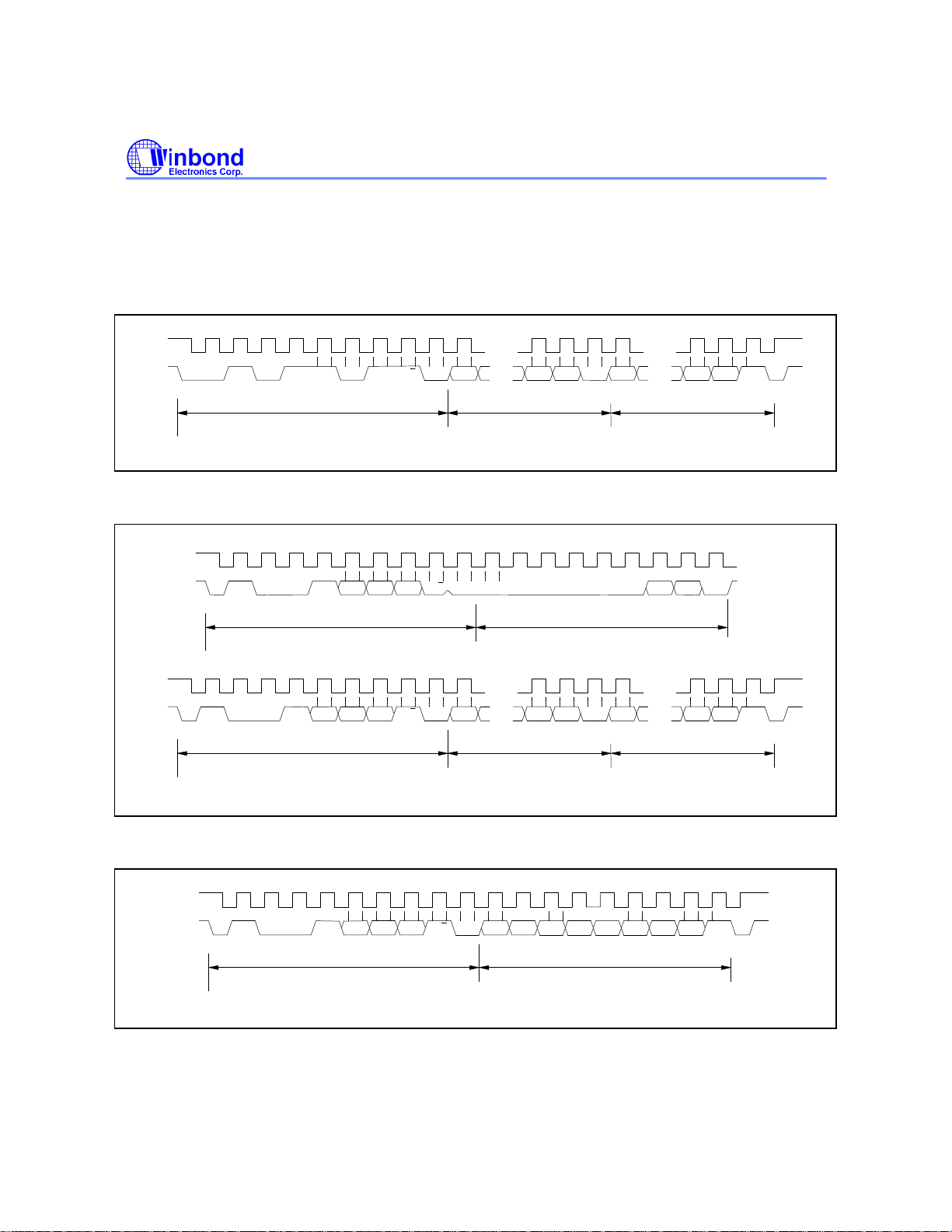
6.2.4 The serial bus timing of the temperature 2 and 3 is shown as follow:
(a) Typical 2-byte read from preset pointer location (Temp, TOS, T
SCL
SDA
0
0 1 0 1 1 0 1 D7 D1 D0
Start By
Master
Frame 1
Serial Bus Address Byte
7 8 0 7 8
R/W
Ack
by
782D
... ...
...
Frame 2
MSB Data Byte
Master
)
HYST
0 7
...
D7 D1 D0
Ack
by
Frame 3
LSB Data Byte
Figure 5. Typical 2-Byte Read From Preset Pointer Location
(b) Typical pointer set followed by immediate read for 2-byte register (Temp, TOS, T
Frame 2
Pointer Byte
Ack
by
Master
4
D1 D0
0 7
D7 D1 D0
...
Frame 5
LSB Data Byte
Ack
by
782D
SCL
SDA
SCL
SDA
Start By
Master
0
1 0 0 1 A2 A1 A0 R/W
Start By
Master
0
1 0 0 1 A2 A1 A0 R/W
Serial Bus Address Byte
Frame 1
Serial Bus Address Byte
Frame 3
7 8 0
0 0 0 0 0 0
Ack
by
782D
7 8 0 7 8
... ...
D7 D1 D0
...
Ack
by
782D
0
Frame 4
MSB Data Byte
Master
HYST
No Ack
by
Master
Stop by
Ack
Master
by
)
Stop by
Master
Figure 6. Typical Pointer Set Followed by Immediate Read for 2-Byte Register
(c) Typical read 1-byte from configuration register with preset pointer
SCL
SDA
0
1 0 0 1 A2 A1 A0 R/W D1D5 D4 D3D6
Start By
Master
Frame 1
Serial Bus Address Byte
Figure 7. Typical 1-Byte Read From Configuration With Preset Pointer
7 8 0
Ack
by
782D
D7 D2
Frame 2
Data Byte
Publication Release Date: April 1999
- 11 - Revision A1
8
7
D0
No Ack
Stop by
by
Master
Master
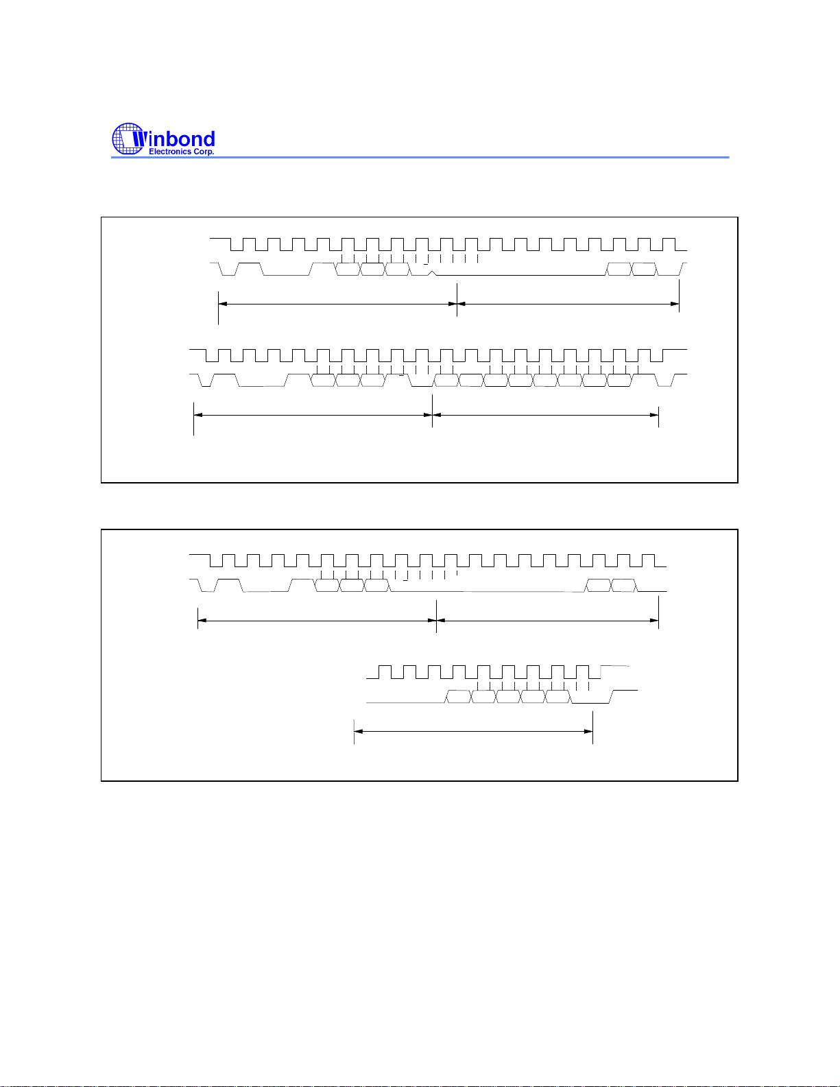
Preliminary W83782D
(d) Typical pointer set followed by immediate read from configuration register
SCL
0
SDA
1 0 0 1 A2 A1 A0 R/W
Start By
Master
Frame 1
Serial Bus Address Byte
0
7 8 0
SCL (Cont..)
SDA (Cont..)
1 0 0 1 A2 A1 A0 R/W
Repea
Start
By
Master
Frame 3
Serial Bus Address Byte
Figure 8. Typical Pointor Set Followed by Immediate Read from Temp 2/3
Configuration Register
(e) Temperature 2/3 configuration register Write
SCL
SDA
0
1 0 0 1 A2 A1 A0 R/W
Start By
Master
Frame 1
Serial Bus Address Byte
7 8 0
7 8 0
0 0 0 0 00
Ack
by
782D
D7 D5 D4
Ack
by
782D
D6 D3
Frame 4
MSB Data Byte
Frame 2
Pointer Byte
4
0 0 0 0 0 0 0
Ack
782D
by
Frame 2
Pointer Byte
4
D2 D1 D0
D1 D0
D1 D0
7
7 8
7 8
8
No Ack
by
Master
Ack
by
782D
782D
Ack
by
Stop by
Master
...
...
SCL (Cont...)
0
SDA (Cont...)
0 0 D4 D3 D2 D10 D0
Frame 3
Configuration Data Byte
Figure 9. Configuration Register Write
- 12 -
7 8
Ack
by
782D
Stop
by
Master
Preliminary W83782D
(f) Temperature 2/3 TOS and T
SCL
SDA
SCL (Cont...)
SDA (Cont...)
0
1 0 0 1 A2 A1 A0 R/W
Start By
Master
Frame 1
Serial Bus Address Byte
0
D6 D5 D4 D3 D2 D1D7 D0
Frame 3
MSB Data Byte
Figure 10. Configuration Register Write
HYST
write
7 8 0
Ack
by
782D
7 8
Ack
by
781D
4
0
0
0 0 0 0
Frame 2
Pointer Byte
7 8
D1 D0
0 7 8
D6 D5 D4 D3 D2 D1D7 D0
Frame 4
LSB Data Byte
Ack
by
782D
Ack
782D
Stop
by
by
Master
Publication Release Date: April 1999
- 13 - Revision A1
Preliminary W83782D
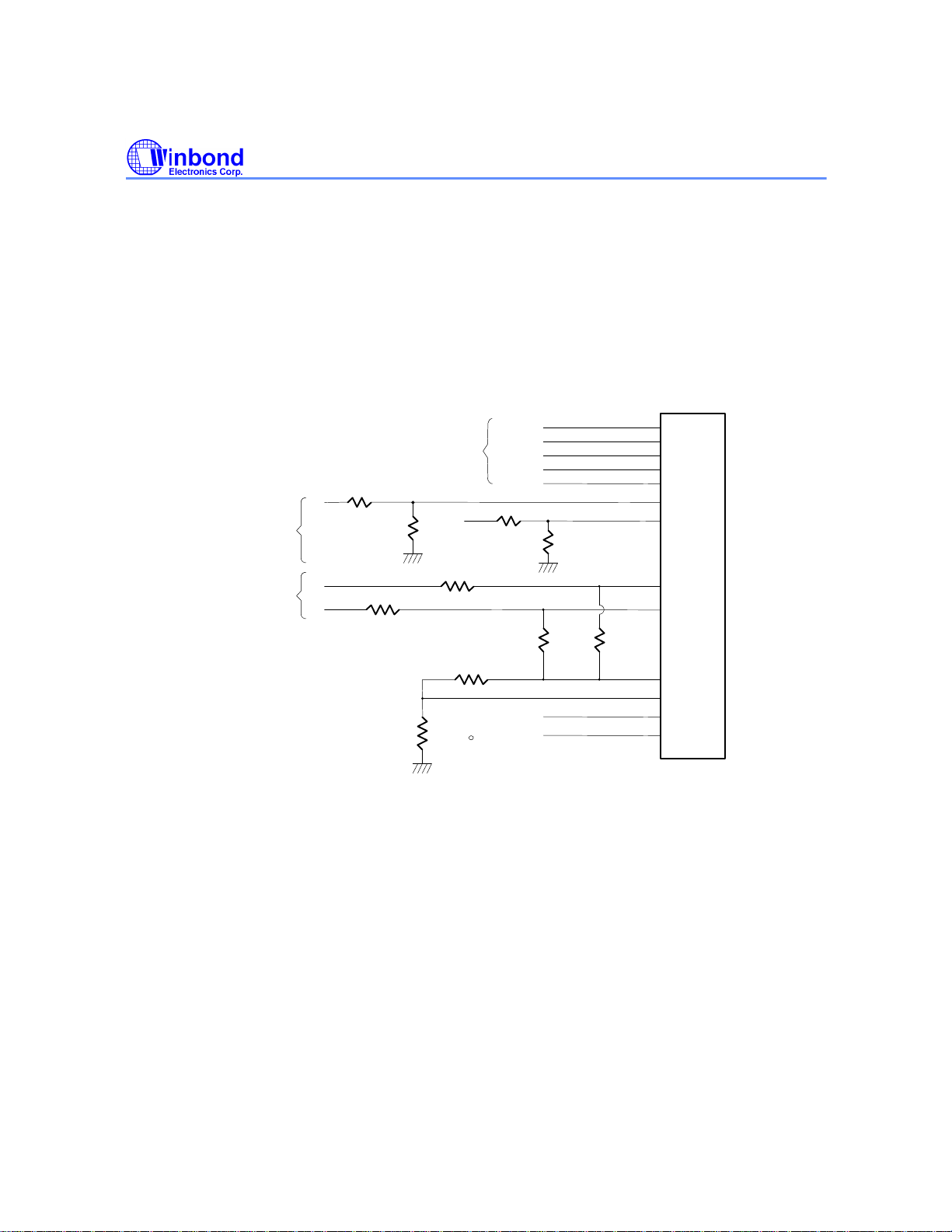
6.3 Analog Inputs
The maximum input voltage of the analog pin is 4.096V because the 8-bit ADC has a 16mv LSB.
Really, the application of the PC monitoring would most often be connected to power suppliers. The
CPU V-core voltage ,+3.3V and battery voltage can directly connected to these analog inputs. The
5VSB and +12V inputs should be reduced a factor with external resistors so as to obtain the input
range. As Figure 11 shows.
V1
Positive Input
Negative Input
Typical Thermister Connection
V3
V4
+2.5VINA
Positive Inputs
R1
R2
R7
R
THM
10K, 25 C
+2.5VINB
+3.3VIN
VDD(+5V)
12VIN
V2
R5
10K, 1%
R
VBAT
R3
R4
N12VIN
N5VIN
R8
VREF Pin 37
VTIN3
VTIN2
VTIN1
**The Connections of VTIN1 and VTIN2
are same as VTIN3
Pin 38
Pin 39
Pin 40
Pin 36
Pin 35
Pin 34
Pin 33
Pin 30
Pin 32
5VSB Pin 29
Pin 31
Pin 28
R6
8-bit ADC
with
16mV LSB
Figure 11.
- 14 -

Preliminary W83782D
Ω
Ω
−
×−β
6.3.1 Monitor over 4.096V voltage:
The input voltage +12VIN can be expressed as following equation.
R
12
VIN V
= ×
1
The value of R1 and R2 can be selected to 28K Ohms and 10K Ohms, respectively, when the input
voltage V1 is 12V. The node voltage of +12VIN can be subject to less than 4.096V for the maximun
input range of the 8-bit ADC. Similarly, the node voltage of 5VSB (measure standby power VSB for
ATX power supply) also can be evaluated by using two series resistors R3 and R4 which real value
can be 5.1K ohms and 7.5K ohms so as to obtain the 5VSB is limited to less than 4.096V. The Pin 33
is connected to the power supply VCC with +5V. There are two functions in this pin with 5V. The first
function is to supply internal analog power in the W83782D and the second function is that this
voltage with 5V is connected to internal serial resistors to monitor the +5V voltage. The value of two
serial resistors are 34K ohms and 50K ohms so that input voltage to ADC is 2.98V which is less than
4.096V of ADC maximum input voltage. The express equation can represent as follows.
V VCC
= ×
in
where VCC is set to 5V.
50
K K
50 34
Ω Ω
R R
K
+
2
+
1 2
≅
2 98
.
V
6.3.2 Monitor negative voltage:
The negative voltage should be connected two series resistors and a positive voltage VREF (is equal
to 3.6V). In the Figure 11, the voltage V3 and V4 are two negative voltage which they are -12V and 5V respectively. The voltage V3 is connected to two serial resistors then is connected to another
terminal VREF which is positive voltage. So as that the voltage node N12VIN can be obtain a
posedge voltage if the scales of the two serial resirtors are carefully selected. It is recommanded from
Winbond that the scale of two serial resistors are R5=232K ohms and R6=56K ohm. the The input
voltage of node -12VIN can be calculated by following equation.
K
N VIN VREF V
If the V5 is equal to -12V then the voltage is equal to 0.567V and the converted hexdecimal data is set
to 35h by the 8-bit ADC with 16mV-LSB.This monitored value should be converted to the real
negative votage and the express equation is shown as follows.
= + ×
where VREF is equal 3.6V.
V
=
5
5 5
N VIN VREF
12
1
- 15 - Revision A1
232
K K
232 56
+
Ω Ω
β
V12
+( ) ( )
Publication Release Date: April 1999

Preliminary W83782D
−
×−γ
Where β is 232K/(232K+56K). If the N2VIN is 0.567 then the V5 is approximately equal to -12V.
The another negative voltage input V6 (approximate -5V) also can be evaluated by the similar
method and the serial resistors can be selected with R7=120K ohms and R8=56K ohms by the
Winbond recommended. The expression equation of V6 With -5V voltage is shown as follows.
N VIN VREF
V
Where the β is set to 120K/(120K+56K). If the monitored ADC value in the N5VIN channel is 0.8635,
VREF=3.6V and the parameter β is 0.6818 then the negative voltage of V6 can be evalated to be -
5V.
6.3.3 Monitor temperature from thermistor:
The W83782D can connect three thermistors to measure three different envirment temperature. The
specification of thermistor should be considered to (1) β value is 3435K, (2) resistor value is 10K
ohms at 25°C. In the Figure 11, the themistor is connected by a serial resistor with 10K Ohms, then
connect to VREF (Pin 37).
5
=
6
1
γ
6.3.4 Monitor temperature from Pentium IITM thermal diode or bipolar transistor 2N3904
The W83782D can alternate the thermistor to Pentium IITM (Deschutes) thermal diode interface or
transistor 2N3904 and the circuit connection is shown as Figure 12. The pin of Pentium IITM D- is
connected to power supply ground (GND) and the pin D+ is connected to pin PIITDx in the W83782D.
The resistor R=30K ohms should be connected to VREF to supply the diode bias current and the
bypass capacitor C=3300pF should be added to filter the high frequency noise. The transistor 2N3904
should be connected to a form with a diode, that is, the Base (B) and Collector (C) in the 2N3904
should be tied togeter to act as a thermal diode.
- 16 -
 Loading...