

Winbond Electronics W83697SF Datasheet

W83697SF
WINBOND I/O

W83697SF Data Sheet Revision History
Pages Dates Version Version
on Web
Main Contents
1 n.a. 04/16/01 0.50 0.50 First published
2 111
04/27/01 0.51 0.51 Update the Top Marking
3
4
5
6
7
8
9
10
Please note that all data and specifications are subject to change without notice. All the
trade marks of products and companies mentioned in this data sheet belong to their
respective owners.
LIFE SUPPORT APPLICATIONS
These products are not designed for use in life support appliances, devices, or systems
where malfunction of these products can reasonably be expected to result in personal
injury. Winbond customers using or selling these products for use in such applications
do so at their own risk and agree to fully indemnify Winbond for any damages resulting
from such improper use or sales.

W83697SF
PRELIMINARY
Publication Release Date: April 2001
- I - Revision 0.50
TABLE OF CONTENT
GENERAL DESCRIPTION .............................................................................................................. 1
PIN CONFIGURATION FOR 697SF................................................................................................ 6
1.0 PIN DESCRIPTION................................................................................................................ 7
1.1 LPC INTERFACE........................................................................................................................ 7
1.2 FDC INTERFACE........................................................................................................................ 9
1.3 MULTI-MODE PARALLEL PORT.....................................................................................................10
1.4 SERIAL PORT INTERFACE............................................................................................................15
1.5 INFRARED PORT ........................................................................................................................16
1.6 FRESH ROM INTERFACE.............................................................................................................16
1.7 GENERAL PURPOSE I/O PORT .....................................................................................................17
1.8 SMART CARD INTERFACE............................................................................................................17
1.9 PWM & GENERAL PURPOSE I/O PORT 8 ...................................................................................... 18
1.10 GAME PORT & MIDI PORT ........................................................................................................18
1.11 POWER PINS...................................................................................................................... 19
2.0 LPC (LOW PIN COUNT) INTERFACE...................................................................................... 20
3.0 FDC FUNCTIONAL DESCRIPTION.........................................................................................21
3.1 W83697SF FDC .....................................................................................................................21
3.1.1 AT interface.....................................................................................................................21
3.1.2 FIFO (Data) .....................................................................................................................21
3.1.3 Data Separator .................................................................................................................22
3.1.4 Write Precompensation.....................................................................................................22
3.1.5 Perpendicular Recording Mode...........................................................................................23
3.1.6 FDC Core ........................................................................................................................23
3.1.7 FDC Commands ...............................................................................................................23
3.2 REGISTER DESCRIPTIONS.............................................................................................................36
3.2.1 Status Register A (SA Register) (Read base address + 0)...................................................36
3.2.2 Status Register B (SB Register) (Read base address + 1)...................................................38
3.2.3 Digital Output Register (DO Register) (Write base address + 2) ............................................40
3.2.4. Tape Drive Register (TD Register) (Read base address + 3) ................................................40
3.2.5 Main Status Register (MS Register) (Read base address + 4)...............................................43
3.2.6 Data Rate Register (DR Register) (Write base address + 4) .................................................43
3.2.7 FIFO Register (R/W base address + 5).............................................................................. 45
3.2.8 Digital Input Register (DI Register) (Read base address + 7)................................................46
3.2.9 Configuration Control Register (CC Register) (Write base address + 7)..................................48
4.0 UART PORT ..........................................................................................................................49

W83697SF
PRELIMINARY
Publication Release Date: April 2001
- II - Revision 0.51
4.1 UNIVERSAL ASYNCHRONOUS RECEIVER /TRANSMITTER (UART A, UART B)..........................................49
4.2 REGISTER ADDRESS ...................................................................................................................49
4.2.1 UART Control Register (UCR) (Read/Write).........................................................................49
4.2.2 UART Status Register (USR) (Read/Write) .........................................................................51
4.2.3 Handshake Control Register (HCR) (Read/Write) .................................................................52
4.2.4 Handshake Status Register (HSR) (Read/Write)..................................................................53
4.2.5 UART FIFO Control Register (SFR) (Write only) ..................................................................54
4.2.6 Interrupt Status Register (ISR) (Read only) .........................................................................55
4.2.7 Interrupt Control Register (ICR) (Read/Write).......................................................................57
4.2.8 Programmable Baud Generator (BLL/BHL) (Read/Write) ...................................................... 57
4.2.9 User-defined Register (UDR) (Read/Write)..........................................................................58
5.0 PARALLEL PORT.................................................................................................................59
5.1 PRINTER INTERFACE LOGIC ..........................................................................................................59
5.2 ENHANCED PARALLEL PORT (EPP).............................................................................................. 60
5.2.1 Data Swapper ...................................................................................................................62
5.2.2 Printer Status BSFfer .......................................................................................................62
5.2.3 Printer Control Latch and Printer Control Swapper................................................................62
5.2.4 EPP Address Port............................................................................................................63
5.2.5 EPP Data Port 0-3............................................................................................................64
5.2.6 Bit Map of Parallel Port and EPP Registers ........................................................................64
5.2.7 EPP Pin Descriptions .......................................................................................................66
5.2.8 EPP Operation.................................................................................................................66
5.3 EXTENDED CAPABILITIES PARALLEL (ECP) PORT............................................................................68
5.3.1 ECP Register and Mode Definitions....................................................................................68
5.3.2 Data and ecpAFifo Port .....................................................................................................69
5.3.3 Device Status Register (DSR)............................................................................................69
5.3.4 Device Control Register (DCR)...........................................................................................70
5.3.5 cFifo (Parallel Port Data FIFO) Mode = 010 ........................................................................71
5.3.6 ecpDFifo (ECP Data FIFO) Mode = 011.............................................................................. 71
5.3.7 tFifo (Test FIFO Mode) Mode = 110...................................................................................71
5.3.8 cnfgA (Configuration Register A) Mode = 111 ......................................................................71
5.3.9 cnfgB (Configuration Register B) Mode = 111 ......................................................................71
5.3.10 ecr (Extended Control Register) Mode = all........................................................................72
5.3.11 Bit Map of ECP Port Registers .........................................................................................73
5.3.12 ECP Pin Descriptions .....................................................................................................75
5.3.13 ECP Operation...............................................................................................................76
5.3.14 FIFO Operation .............................................................................................................. 76
5.3.15 DMA Transfers ...............................................................................................................77
5.3.16 Programmed I/O (NON- DMA) Mode..................................................................................77
5.4 EXTENSION FDD MODE (EXTFDD)...............................................................................................77
5.5 EXTENSION 2FDD MODE (EXT2FDD)...........................................................................................77
6.0 GENERAL PURPOSE I/O.......................................................................................................78
7.0 ACPI REGISTERS FEATURES ...............................................................................................82

W83697SF
PRELIMINARY
Publication Release Date: April 2001
- III - Revision 0.51
8.0 PULSE WIDTH MODULATION (PWM)....................................................................................83
8.1 GENERAL DESCRIPTION...............................................................................................................83
8.2 LPC INTERFACE.......................................................................................................................83
8.3 REGISTERS ..........................................................................................................................84
8.3.1 Address Register (Port x5h)...............................................................................................84
8.3.2 Data Register (Port x6h) ....................................................................................................84
8.3.3 PWM 1 Pre-Scale Register -- Index 00h ..............................................................................85
8.3.4 PWM 1 Duty Cycle Select Register – Index 01h ..................................................................85
8.3.5 PWM 2 Pre-Scale Register -- Index 02h ..............................................................................86
8.3.6 PWM 2 Duty Cycle Select Register -- Index 03h ..................................................................86
8.3.7 PWM 0 Pre-Scale Register -- Index 10h ..............................................................................87
8.3.8 PWM 0 Duty Cycle Select Register – Index 11h..................................................................87
9.0 CONFIGURATION REGISTER................................................................................................88
9.1 PLUG AND PLAY C ONFIGURATION ................................................................................................88
9.2 COMPATIBLE PNP.....................................................................................................................88
9.2.1 Extended Function Registers.............................................................................................88
9.2.2 Extended Functions Enable Registers (EFERs) ..................................................................89
9.2.3 Extended Function Index Registers (EFIRs), Extended Function Data Registers(EFDRs)........89
9.3 CONFIGURATION SEQUENCE .........................................................................................................89
9.3.1 Enter the extended function mode ......................................................................................89
9.3.2 Configurate the configuration registers ................................................................................89
9.3.3 Exit the extended function mode........................................................................................89
9.3.4 Software programming example .........................................................................................90
9.4 CHIP (G LOBAL) CONTROL REGISTER .............................................................................................91
9.5 LOGICAL DEVICE 0 (FDC)...........................................................................................................99
9.6 LOGICAL DEVICE 1 (PARALLEL PORT)......................................................................................... 103
9.7 LOGICAL DEVICE 2 (UART A)....................................................................................................104
9.8 LOGICAL DEVICE 3 (UART B)....................................................................................................105
9.9 LOGICAL DEVICE 7 (GAME PORT AND GPIO PORT 1).....................................................................107
9.10 LOGICAL DEVICE 8 (MIDI PORT AND GPIO PORT 5).....................................................................108
9.11 LOGICAL DEVICE 9 (GPIO PORT 2 ~ GPIO PORT 4 )...................................................................110
9.12 LOGICAL DEVICE A (ACPI)......................................................................................................111
9.13 LOGICAL DEVICE B (PWM).....................................................................................................117
9.14 LOGICAL DEVICE C (SMART CARD)........................................................................................ 117
9.15 LOGICAL DEVICE D (URC & GPIO PORT 6 )..............................................................................118
9.16 LOGICAL DEVICE E (URD & GPIO PORT 7 ).............................................................................. 119
9.17 LOGICAL DEVICE F (GPIO PORT 8) ..........................................................................................120
10.0 ORDERING INSTRUCTION................................................................................................. 122
11.0 HOW TO READ THE TOP MARKING ..................................................................................122
12.0 PACKAGE DIMENS IONS ....................................................................................................123

W83697SF
PRELIMINARY
Publication Release Date: April 2001
- 1 - Revision 0.50
GENERAL DESCRIPTION
The W83697SF is evolving product from Winbond's most popular I/O family. They feature a whole new
interface, namely LPC (Low Pin Count) interface, which will be supported in the new generation chip-
set. This interface as its name suggests is to provide an economical implementation of I/O's interface
with lower pin count and still maintains equivalent performance as its ISA interface counterpart.
Approximately 40 pin counts are saved in LPC I/O comparing to ISA implementation. With this
additional freedom, we can implement more devices on a single chip as demonstrated in W83697SF's
integration of Game Port and MIDI Port. It is fully transparent in terms of software which means no BIOS
or device driver update is needed except chip-specific configuration.
As Smart Card application is gaining more and more attention, W83697SF also implements a smart
card reader interface featuring Smart wake -up function. This smart card reader interface fully meets the
ISO7816 and PC/SC (Personal Computer/Smart Card Workgroup) standards. W83697SF provides a
minimum extern al components and lowest cost solution for smart card applications.
The disk drive adapter functions of W83697SF include a floppy disk drive controller compatible with the
industry standard 82077/ 765, data separator, write pre-compensation circuit, decode logic, data rate
selection, clock generator, drive interface control logic, and interrupt and DMA logic. The wide range of
functions integrated onto the W83697SF greatly reduces the number of components required for
interfacing with floppy disk drives. The W83697SF supports four 360K, 720K, 1.2M, 1.44M, or 2.88M
disk drives and data tranSFer rates of 250 Kb/s, 300 Kb/s, 500 Kb/s,1 Mb/s, and 2 Mb/s.
The W83697SF provides two high-speed serial communication ports (UARTs), one of which supports
serial Infrared communication. Each UART includes a 16-byte send/receive FIFO, a programmable baud
rate generator, complete modem control capability, and a processor interrupt system. Both UARTs
provide legacy speed with baud rate up to 115.2k bps and also advanced speed with baud rates of 230k,
460k, or 921k bps which support higher speed modems. In addition, the W83697SF provides IR
functions: IrDA 1.0 (SIR for 1.152K bps) and TV remote IR (Consumer IR, supporting NEC, RC-5,
extended RC-5, and RECS -80 protocols).
The W83697SF supports one PC-compatible printer port (SPP), Bi-directional Printer port (BPP) and
also Enhanced Parallel Port (EPP) and Extended Capabilities Port (ECP). Through the printer port
interface pins, also available are: Extension FDD Mode and Ext ension 2FDD Mode allowing one or two
external floppy disk drives to be connected.
The configuration registers support mode selection, function enable/disable, and power down function
selection. Furthermore, the configurable PnP features are compatible with the plug-and -play feature
demand of Windows 95/98TM, which makes system resource allocation more efficient than ever.
The W83697SF provides a set of flexible I/O control functions to the system designer through a set of
General Purpose I/O ports. These GPIO ports may serve as simple I/O or may be individually configured

W83697SF
PRELIMINARY
Publication Release Date: April 2001
- 2 - Revision 0.51
to provide a predefined alternate function. General Purpose Port 1 is designed to be functional even in
power down mode (VCC is off).
The W83697SF is made to fully comply with Microsoft PC98 and PC99 Hardware Design Guide,
and meet the requirements of ACPI.
The W83697SF contains a game port and a MIDI port. The game port is designed to support 2 joysticks
and can be applied to all standard PC game control devices, They are very important for a entertainment
or consumer computer.
The W83697SF provides Flash ROM interface . That can support up to 4M legacy flash ROM.
Moreover, W83697SF support 3 sets PWM Fan Speed Control, which are very important for a high-
end computer system to work stably and properly.

W83697SF
PRELIMINARY
Publication Release Date: April 2001
- 3 - Revision 0.51
FEATURES
General
• Meet LPC Spec. 1.01
• Support LDRQ#(LPC DMA), SERIRQ (serial IRQ)
• Include all the features of Winbond I/O W83877TF
• Integrate Smart Card functions
• Compliant with Microsoft PC98/PC99 Hardware Design Guide
• Support DPM (Device Power Management), ACPI
• Programmable configuration settings
• Single 24 or 48 MHz clock input
FDC
• Compatible with IBM PC AT disk drive systems
• Variable write pre- compensation with track selectable capability
• Support vertical recording format
• DMA enable logic
• 16 -byte data FIFOs
• Support floppy disk drives and tape drives
• Detects all overrun and underrun conditions
• Built-in address mark detection circuit to simplify the read electronics
• FDD anti -virus functions with software write protect and FDD write enable signal (write data signal
was forced to be inactive)
• Support up to four 3.5 -inch or 5.25-inch floppy disk drives
• Completely compatible with industry standard 82077
• 360K/720K/1.2M/1.44M/2.88M format; 250K, 300K, 500K, 1M, 2M bps data transfer rate
• Support 3-mode FDD, and its Win95/98 driver
UART
• Two high-speed 16550 compatible UARTs with 16-byte send/receive FIFOs
• MIDI compatible
• Fully programmable serial -interface characteristics:
--- 5, 6, 7 or 8-bit characters
--- Even, odd or no parity bit generation/detection
--- 1, 1.5 or 2 stop bits generation

W83697SF
PRELIMINARY
Publication Release Date: April 2001
- 4 - Revision 0.51
• Internal diagnostic capabilities:
--- Loop-back controls for communications link fault isolation
--- Break, parity, overrun, framing error simulation
• Programmable baud generator allows division of 1.8461 MHz and 24 MHz by 1 to (216-1)
• Maximum baud rate up to 921k bps for 14.769 MHz and 1.5M bps for 24 MHz
Infrared
• Support IrDA version 1.0 SIR protocol with maximum baud rate up to 115.2K bps
• Support SHARP ASK-IR protocol with maximum baud rate up to 57,600 bps
• Support Consumer IR with Wake-Up function.
Parallel Port
• Compatible with IBM parallel port
• Support PS/2 compatible bi-directional parallel port
• Support Enhanced Parallel Port (EPP) − Compatible with IEEE 1284 specification
• Support Extended Capabilities Port (ECP) − Compatible with IEEE 1284 specification
• Extension FDD mode supports disk drive B; and Extension 2FDD mode supports disk drives A and
B through parallel port
• Enhanced printer port back -drive current protection

W83697SF
PRELIMINARY
Publication Release Date: April 2001
- 5 - Revision 0.51
Game Port
• Support two separate Joysticks
• Support every Joystick two axes (X,Y) and two buttons (S1,S2) controllers
MIDI Port
• The baud rate is 31.25 Kbaud
• 16 -byte input FIFO
• 16 -byte output FIFO
Flash ROM Interface
• Support up to 4M flash ROM
General Purpose I/O Ports
• 60 programmable general purpose I/O ports
• General purpose I/O ports can serve as simple I/O ports, watch dog timer output, power LED
output, infrared I/O pins, suspend LED output, Beep output
• Functional in power down mode
Smart Card Reader Interface
• ISO7816 protocol compliant
• PC/SC T=0, T=1 compliant
Fan Speed Control
• 3 Sets PWM Fan Speed Control
Package
• 128 -pin PQFP
W83697SF
PRELIMINARY
Publication Release Date: April 2001
- 6 - Revision 0.51
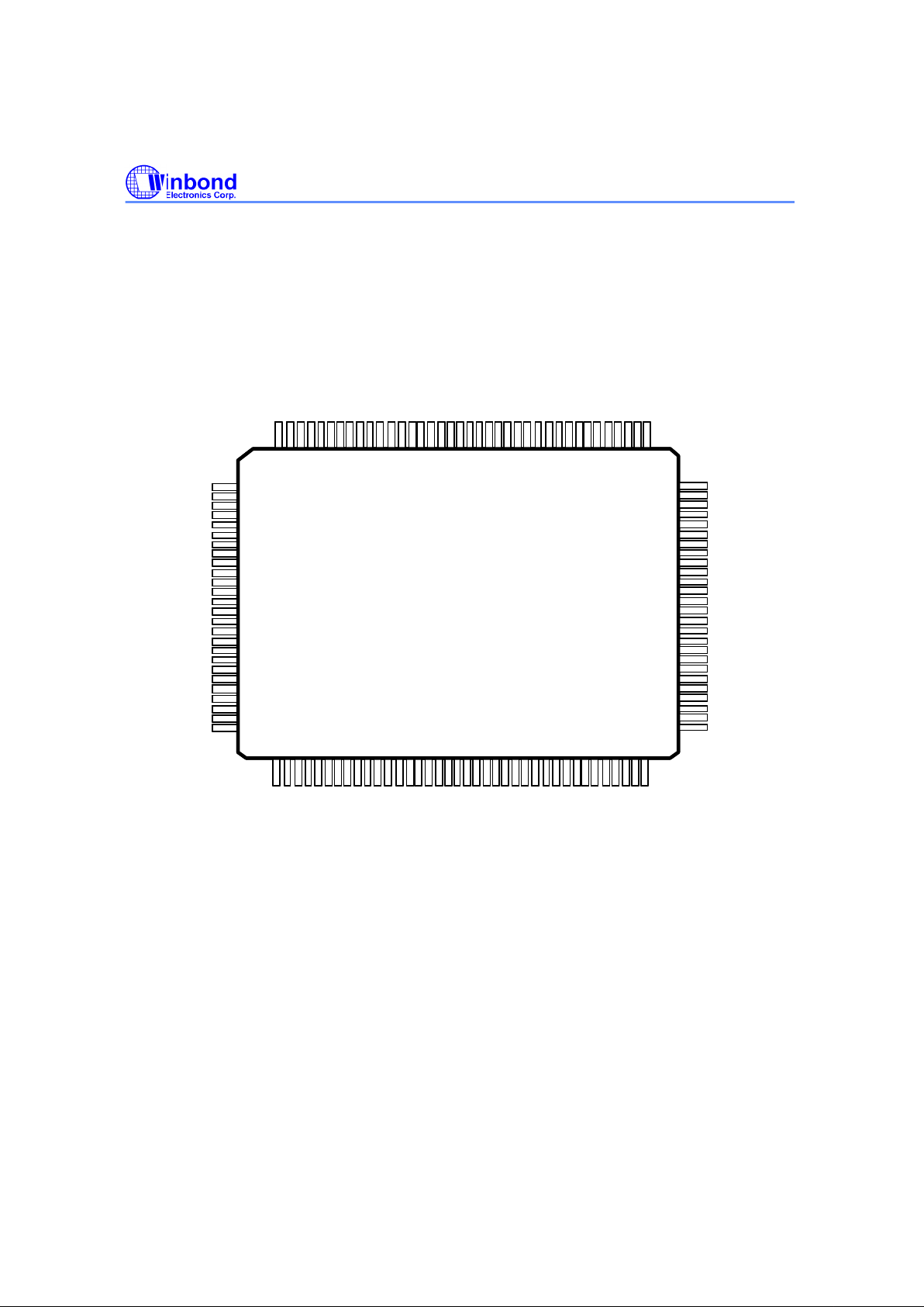
PIN CONFIGURATION FOR 697SF
64
63
62
61
60
59
58
57
56
55
54
53
52
51
50
49
48
47
46
45
44
43
42
41
40
39
103
104
105
106
107
108
109
110
111
112
113
114
115
116
117
118
119
120
121
122
123
124
125
126
127
128
2 1 0
1
0101099
989
7
969594939
29190898887
868
5
8483828180797
8777675
747
3
727
1706968676665
1 2 3 4 5 6 7 8 91011121314151617181920212223242526272829303132333435363738
DRVDEN0
INDEX#
GND
MOA#
DSB#
DSA#
MOB#
STEP#
DIR#
WD#
WE#
VCC
TRAK0#
WP#
RDATA#
HEAD#
DSKCHG#
CLKIN#
PME#
SLIN#
PCICLK
LDRQ#
SERIRQ
LAD3
LAD2
LAD1
VCC3
LAD0
LFRAME#
LRESET#
SLCT
PE
BUSY
ACK#
PD4
PD5
PD7
PD6
RIB#
DCDB#
SOUTB
SINB
GND
DTRB#
RTSB#
RIA#
DCDA#
CTSB#
SOUTA
SINA
DTRA#
RTSA#
DSRA#
CTSA#
VCC
STB#
AFD#
DSRB#
INIT#
PD0
PD1
PD2
PD3
IRTX
XA18/GP57
VCC
XA17/GP56
XA16/GP55
MEMR#/GP53
MEMW#/GP52
GP64
ROMCS#/GP54
GP65
GP66
GP67
GND
GP63
GP62
GP61
GP60
SCPSNT/GP77
SCIO/GP76
SCCLK/GP75
SCRST/GP74
GP73
SCC8/GP72
SCPWR/GP71
SCC4/GP70
PWM1/GP82
PWM2/PLED/GP83
PWM0/GP81
WDTO/GP80
MSI/GP51
MSO/GP50
GPAS2/GP17
GPBS2/GP16
GPAY/GP15
GPBY/GP14
GPBX/GP13
GPAX/GP12
GPBS1/GP11
GPAS1/GP10
IRRX
ERR#
XA15/GP47
XA14/GP46
XA13/GP45
XA12/GP44
XA11/GP43
XA10/GP42
XA9/GP41
XA8/GP40
XA7/GP37
XA6/GP36
XA5/GP35
XA4/GP34
XA3/GP33
XA2/GP32
XA0/GP30
XA1/GP31
XD7/GP27
XD6/GP26
XD5/GP25
XD4/GP24
XD3/GP23
XD2/GP22
XD1/GP21
XD0/GP20
W83697SF
64
63
62
61
60
59
58
57
56
55
54
53
52
51
50
49
48
47
46
45
44
43
42
41
40
64
63
62
61
60
59
58
57
56
55
54
53
52
51
50
49
48
47
46
45
44
43
42
41
40
39
103
104
105
106
107
108
109
110
111
112
113
114
115
116
117
118
119
120
121
122
123
124
125
126
127
128
2 1 0
1
0101099
989
7
969594939
29190898887
868
5
8483828180797
8777675
747
3
727
1706968676665
1 2 3 4 5 6 7 8 910101111121213131414151516161717181819192020212122222323242425252626272728282929303031313232333334343535363637373838
DRVDEN0
INDEX#
GND
MOA#
DSB#
DSA#
MOB#
STEP#
DIR#
WD#
WE#
VCC
TRAK0#
WP#
RDATA#
HEAD#
DSKCHG#
CLKIN#
PME#
SLIN#
PCICLK
LDRQ#
SERIRQ
LAD3
LAD2
LAD1
VCC3
LAD0
LFRAME#
LRESET#
SLCT
PE
BUSY
ACK#
PD4
PD5
PD7
PD6
RIB#
DCDB#
SOUTB
SINB
GND
DTRB#
RTSB#
RIA#
DCDA#
CTSB#
SOUTA
SINA
DTRA#
RTSA#
DSRA#
CTSA#
VCC
STB#
AFD#
DSRB#
INIT#
PD0
PD1
PD2
PD3
IRTX
XA18/GP57
VCC
XA17/GP56
XA16/GP55
MEMR#/GP53
MEMW#/GP52
GP64
ROMCS#/GP54
GP65
GP66
GP67
GND
GP63
GP62
GP61
GP60
SCPSNT/GP77
SCIO/GP76
SCCLK/GP75
SCRST/GP74
GP73
SCC8/GP72
SCPWR/GP71
SCC4/GP70
PWM1/GP82
PWM2/PLED/GP83
PWM0/GP81
WDTO/GP80
MSI/GP51
MSO/GP50
GPAS2/GP17
GPBS2/GP16
GPAY/GP15
GPBY/GP14
GPBX/GP13
GPAX/GP12
GPBS1/GP11
GPAS1/GP10
IRRX
ERR#
XA15/GP47
XA14/GP46
XA13/GP45
XA12/GP44
XA11/GP43
XA10/GP42
XA9/GP41
XA8/GP40
XA7/GP37
XA6/GP36
XA5/GP35
XA4/GP34
XA3/GP33
XA2/GP32
XA0/GP30
XA1/GP31
XD7/GP27
XD6/GP26
XD5/GP25
XD4/GP24
XD3/GP23
XD2/GP22
XD1/GP21
XD0/GP20
W83697SF
W83697SF
PRELIMINARY
Publication Release Date: April 2001
- 7 - Revision 0.51
1.0 PIN DESCRIPTION
Note: Please refer to Section 13.2 DC CHARACTERISTICS for details.
I/O8t - TTL level bi-directional pin with 8 mA source-sink capability
I/O
16t
- TTL level bi-directional pin with 16 mA source-sink capability
I/O12ts - TTL level output pin with 12 mA sou rce-sink capability and Schmitt-trigger input pin
I/O
16ts
- TTL level output pin with 16 mA source -sink capability and Schmitt-trigger input pin
I/O
24cs
- TTL level output pin with 24 mA source-sink capability and CMOS level Schmitt-trigger input pin
I/OD
16t
- TTL level open-drain output pin with 16 mA source-sink capability and input pin
I/OD
24cs
- TTL level open-drain output pin with 24 mA source-sink capability and CMOS level Schmitt-trigger input pin
I/O
24tp3
- 3.3V TTL level bi-directional pin with 24 mA source -sink capability
O16 - Output pin with 16 mA source -sink capability
O24 - Output pin with 24 mA source -sink capability
OD8 - Open-drain output pin with 8 mA sink capability
OD16 - Open-drain output pin with 16 mA sink capability
OD20 - Open-drain output pin with 20 mA sink capability
OD24 - Open-drain output pin with 24 mA sink capability
O
24p3
- 3.3V output pin with 24 mA source-sink capability
INt - TTL level input pin
INts - TTL level Schmitt -trigger input pin
INcs - CMOS level Schmitt-trigger input pin
IN
tsp3
- 3.3V TTL level Schmitt-trigger input pin
1.1 LPC Interface
SYMBOL PIN I/O FUNCTION
CLKIN 17 INt System clock input. According to the input frequency 24MHz or
48MHz, it is selectable through register. Default is 24MHz input.
PME#
98 OD16 Generated PME event.
PCICLK 19 IN
tsp3
PCI clock input.
LDRQ# 20 O
24p3
Encoded DMA Request signal.
SERIRQ 21 I/O
24tp3
Serial IRQ input/Output.
LAD[3:0] 23-26 I/O
24tp3
These signal lines communicate address, control, and data
information over the LPC bus between a host and a peripheral.
LFRAME#
27 IN
tsp3
Indicates start of a new cycle or termination of a broken cycle.

W83697SF
PRELIMINARY
Publication Release Date: April 2001
- 8 - Revision 0.51
LRESET#
28 IN
tsp3
Reset signal. It can connect to PCIRST# signal on the host.
W83697SF
PRELIMINARY
Publication Release Date: April 2001
- 9 - Revision 0.51
1.2 FDC Interface
SYMBOL PIN I/O FUNCTI ON
DRVDEN0 1 OD24 Drive Density Select bit 0.
INDEX#
2 INcs This Schmitt- triggered input from the disk drive is active low when
the head is positioned over the beginning of a track marked by an
index hole. This input pin is pulled up internally by a 1 KΩ
resistor. The resistor can be disabled by bit 7 of L0-CRF0
(FIPURDWN).
MOA#
3 OD24 Motor A On. When set to 0, this pin enables disk drive 0. This is
an open drain output.
DSB#
4 OD24 Drive Select B. When set to 0, this pin enables disk drive B. This
is an open drain output.
DSA#
6 OD24 Drive Select A. When set to 0, this pin enables disk drive A. This
is an open drain output.
MOB#
7 OD24 Motor B On. When set to 0, this pin enables disk drive 1. This is
an open drain output.
DIR#
8 OD24 Dire ction of the head step motor. An open drain output.
Logic 1 = outward motion
Logic 0 = inward motion
STEP#
9 OD24 Step output pulses. This active low open drain output produces a
pulse to move the head to another track.
WD#
10 OD
24
Write data. This logic low open drain writes pre-compensation
serial data to the selected FDD. An open drain output.
WE#
11 OD24 Write enable. An open drain output.
TRAK0#
12 INcs Track 0. This Schmitt-triggered input from the disk drive is active
low when the head is positioned over the outermost track. This
input pin is pulled up internally by a 1 KΩ resistor. The resistor
can be disabled by bit 7 of L0- CRF0 (FIPURDWN).
WP#
13 INcs Write protected. This active low Schmitt input from the disk drive
indicates that the diskette is write-protected. This input pin is
pulled up internally by a 1 KΩ res istor. The resistor can be
disabled by bit 7 of L0-CRF0 (FIPURDWN).
RDATA#
14 INcs The read data input signal from the FDD. This input pin is pulled
up internally by a 1 KΩ resistor. The resistor can be disabled by
bit 7 of L0-CRF0 (FIPURDWN).
W83697SF
PRELIMINARY
Publication Release Date: April 2001
- 10 - Revision 0.51
1.2 FDC Interface, continued
SYMBOL PIN I/O FUNCTION
HEAD#
15 OD24 Head select. This open drain output determines which disk drive
head is active.
Logic 1 = side 0
Logic 0 = side 1
DSKCHG#
16 INcs Diskette change. This signal is active low at power on and
wh enever the diskette is removed. This input pin is pulled up
internally by a 1 KΩ resistor. The resistor can be disabled by bit 7
of L0 -CRF0 (FIPURDWN).
1.3 Multi-Mode Parallel Port
The following pins have alternate functions, which are controlled by CR28 and L3-CRF0.
SYMBOL PIN I/O FUNCTION
SLCT 29 INt
PRINTER MODE:
An active high input on this pin indicates that the printer is
selected. This pin is pulled high internally. Refer to the
description of the parallel port for definition of this pin in ECP and
EPP mode.
OD12
EXTENSION FDD MODE: WE2#
This pin is for Extension FDD B; its function is the same as the
WE#
pin of FDC.
OD12
EXTENSION 2FDD MODE: WE2#
This pin is for Extension FDD A and B; its function is the same as
the
WE#
pin of FDC.
PE
30 INt
PRINTER MODE:
An active high input on this pin indicates that the printer has
detected the end of the paper. This pin is pulled high internally.
Refer to the description of the parallel port for the definition of this
pin in ECP and EPP mode.
OD12
EXTENSION FDD MODE: WD2#
This pin is for Extension FDD B; its fu nction is the same as the
WD#
pin of FDC.
OD
12
EXTENSION 2FDD MODE: WD2#
This pin is for Extension FDD A and B; its function is the same as
the
WD#
pin of FDC.

W83697SF
PRELIMINARY
Publication Release Date: April 2001
- 11 - Revision 0.51
1.3 Multi-Mode Parallel Port, continued
SYMBOL PIN I/O FUNCTION
BUSY 31 INt
PRINTER MODE:
An active high input indicates that the printer is not ready to
receive data. This pin is pulled high internally. Refer to the
description of the parallel port for definition of this pin in ECP and
EPP mode.
OD12
EXTENSION FDD MODE: MOB2#
This pin is for Extension FDD B; its function is the same as the
MOB# pin of FDC.
OD
12
EXTENSION 2FDD MODE: MOB2#
This pin is for Extension FDD A and B; its function is the same as
the MOB# pin of FDC.
ACK# 32 INt
OD12
OD
12
PRINTER MODE: ACK#
An active low input on this pin indicates that the printer has
received data and is ready to accept more data. This pin is pulled
high internally. Refer to the description of the parallel port for the
definition of this pin in ECP and EPP mode.
EXTENSION FDD MODE: DSB2#
This pin is for the Extension FDD B; its functions is the same as
the DSB# pin of FDC.
EXTENSION 2FDD MODE: DSB2#
This pin is for Extension FDD A and B; its function is the same as
the DSB# pin of FDC.
ERR#
33
INt
OD12
OD12
PRINTER MODE: ERR#
An active low input on this pin indicates that the printer has
encountered an error condition. This pin is pulled high internally.
Refer to the description of the parallel port for the definition of this
pin in ECP and EPP mode.
EXTENSION FDD MODE: HEAD2#
This pin is for Extension FDD B; its function is the same as the
HEAD#pin of FDC.
EXTENSION 2FDD MODE: HEAD2#
This pin is for Extension FDD A and B; its function is the same as
the HEAD# pin of FDC.

W83697SF
PRELIMINARY
Publication Release Date: April 2001
- 12 - Revision 0.51
1.3 Multi-Mode Parallel Port, continued
SYMBOL PIN I/O FUNCTION
SLIN# 34 OD12
OD12
OD12
PRINTER MODE: SLIN#
Output line for detection of printer selection. This pin is pulled high
internally. Refer to the description of the parallel port for the
definition of this pin in ECP and EPP mode.
EXTENSION FDD MODE: STEP2#
This pin is for Extension FDD B; its function is the same as the
STEP# pin of FDC.
EXTENSION 2FDD MODE: STEP2#
This pin is for Extension FDD A and B; its function is the same as
the STEP# pin of FDC.
INIT#
43 OD12
OD12
OD12
PRINTER MODE: INIT#
Output line for the printer initialization. This pin is pulled high
internally. Refer to the description of the parallel port for the
definition of this pin in ECP and EPP mode.
EXTENSION FDD MODE: DIR2#
This pin is for Extension FDD B; its function is the same as the
DIR# pin of FDC.
EXTENSION 2FDD MODE: DIR2#
This pin is for Extension FDD A and B; its function is the same as
the DIR# pin of FDC.
AFD# 44 OD12
OD
12
OD12
PRINTER MODE: AFD#
An active low output from this pin causes the printer to auto feed a
line after a line is printed. This pin is pulled high internally. Refer to
the description of the parallel port for the definition of this pin in
ECP and EPP mode.
EXTENSION FDD MODE: DRVDEN0
This pin is for Extension FDD B; its function is the same as the
DRVDEN0 pin of FDC.
EXTENSION 2FDD MODE: DRVDEN0
This pin is for Extension FDD A and B; its function is the same as
the DRVDEN0 pin of FDC.

W83697SF
PRELIMINARY
Publication Release Date: April 2001
- 13 - Revision 0.51
1.3 Multi-Mode Parallel Port, continued
SYMBOL PIN I/O FUNCTION
STB# 46 OD12 PRINTER MODE: STB#
An active low output is used to latch the parallel data into the
printer. This pin is pulled high internally. Refer to the description of
the parallel port for the definition of this pin in ECP and EPP mode.
- EXTENSION FDD MODE: This pin is a tri-state output.
- EXTENSION 2FDD MODE: This pin is a tri-state output.
PD0
42 I/O
12t
PRINTER MODE: PD0
Parallel port data bus bit 0. Refer to the description of the parallel
port for the definition of this pin in ECP and EPP mode.
INt
EXTENSION FDD MODE: INDEX2#
This pin is for Extension FDD B; its function is the same as the
INDEX# pin of FDC. It is pulled high internally.
INt EXTENSION 2FDD MODE: INDEX2#
This pin is for Extension FDD A and B; its function is the same as
the INDEX# pin of FDC. It is pulled high internally.
PD1
41 I/O
12t
INt
INt
PRINTER MODE: PD1
Parallel port data bus bit 1. Refer to the description of the parallel
port for the definition of this pin in ECP and EPP mode.
EXTENSION FDD MODE: TRAK02#
This pin is for Extension FDD B; its function is the same as the
TRAK0# pin of FDC. It is pulled high internally.
EXTENSION. 2FDD MODE: TRAK02#
This pin is for Extension FDD A and B; its function is the same as
the TRAK0# pin of FDC. It is pulled high internally.
PD2
40 I/O
12t
INt
IN
t
PRINTER MODE: PD2
Parallel port data bus bit 2. Refer to the description of the parallel
port for the definition of this pin in ECP and EPP mode.
EXTENSION FDD MODE: WP2#
This pin is for Extension FDD B; its function is the same as the
WP# pin of FDC. It is pulled high internally.
EXTENSION. 2FDD MODE: WP2#
This pin is for Extension FDD A and B; its function is the same as
the WP# pin of FDC. It is pulled high internally.

W83697SF
PRELIMINARY
Publication Release Date: April 2001
- 14 - Revision 0.51
1.3 Multi-Mode Parallel Port, continued
SYMB OL PIN I/O FUNCTION
PD3
39 I/O
12t
INt
INt
PRINTER MODE: PD3
Parallel port data bus bit 3. Refer to the description of the parallel
port for the definition of this pin in ECP and EPP mode.
EXTENSION FDD MODE: RDATA2#
This pin is for Extension FDD B; its function is the same as the
RDATA# pin of FDC. It is pulled high internally.
EXTENSION 2FDD MODE: RDATA2#
This pin is for Extension FDD A and B; its function is the same as
the RDATA# pin of FDC. It is pulled high internally.
PD4
38 I/O
12t
INt
INt
PRINTER MODE: PD4
Parallel port data bus bit 4. Refer to the description of the parallel
port for the definition of this pin in ECP and EPP mode.
EXTENSION FDD MODE: DSKCHG2#
This pin is for Extension FDD B; the function of this pin is the same
as the DSKCHG# pin of FDC. It is pulled high internally.
EXTENSION 2FDD MODE: DSKCHG2#
This pin is for Extension FDD A and B; this function of this pin is
the same as the DSKCHG# pin of FDC. It is pulled high internally.
PD5
37 I/O
12t
-
-
PRINTER MODE: PD5
Parallel port data bus bit 5. Refer to the description of the parallel
port for the definition of this pin in ECP and EPP mode.
EXTENSION FDD MODE: This pin is a tri- state output.
EXTENSION 2FDD MODE: This pin is a tri-state output.
PD6
36 I/OD
12t
-
OD12
PRINTER MODE: PD6
Parallel port data bus bit 6. Refer to the description of the parallel
port for the definition of this pin in ECP and EPP mode.
EXTENSION FDD MODE: This pin is a tri- state output.
EXTENSION. 2FDD MODE: MOA2#
This pin is for Exten sion FDD A; its function is the same as the
MOA# pin of FDC.
PD7
35 I/OD
12t
-
OD12
PRINTER MODE: PD7
Parallel port data bus bit 7. Refer to the description of the parallel
port for the definition of this pin in ECP and EPP mode.
EXTENSION FDD MODE: This pin is a tri- state output.
EXTENSION 2FDD MODE: DSA2#
This pin is for Extension FDD A; its function is the same as the
DSA# pin of FDC.
W83697SF
PRELIMINARY
Publication Release Date: April 2001
- 15 - Revision 0.51
1.4 Serial Port Interface
SYMBOL PIN I/O FUNCTION
CTSA#
CTSB#
47
55
INt Clear To Send. It is the modem control input.
The function of these pins can be tested by reading bit 4 of the
handshake status register.
DSRA#
DSRB#
48
56
INt Data Set Ready. An active low signal indicates the modem or data
set is ready to establish a communication link and transfer data to
the UART.
RTSA#
49
I/O8t UART A Request To Send. An active low signal informs the modem
or data set that the controller is ready to send data.
HEFRAS
During power-on reset, this pin is pulled down internally and is
defined as HEFRAS, which provides the power-on value for CR26 bit
6 (HEFRAS). A 4.7 kΩ is recommended if intends to pull up.
(select 4EH as configuration I/O port′s address)
RTSB#
57 I/O8t UART B Request To Send. An active low signal informs the modem
or data set that the controller is ready to send data.
DTRA#
PNPCSV#
50
I/O8t UART A Data Terminal Ready. An active low signal informs the
modem or data set that the controller is ready to communicate.
During power- on reset, this pin is pulled down internally and is
defined as
PNPCSV#
, which provides the power-on value for CR24
bit 0 (
PNPCSV#
). A 4.7 kΩ is recommended if intends to pull up.
(clear the default value of FDC, UARTs, and PRT)
DTRB#
58
I/O
8t
UART B Data Terminal Ready. An active low signal informs the
modem or data set that controller is ready to communicate.
SINA
SINB
51
59
INt Serial Input. It is used to receive serial data through the
communication link.
SOUTA
PENROM#
52
I/O8t UART A Serial Output. It is used to transmit serial data out to the
communication link.
During power on reset , this pin is pulled down internally and is
defined as PENROM#, which provides the power on value for CR24
bit 1. A 4.7kΩ is recommended if intends to pull up .
SOUTB
PEN48
61
I/O8t UART B Serial Output. During power-on reset, this pin is pulled
down internally and is defined as PEN48, which provides the poweron value for CR24 bit 6 (EN48). A 4.7 kΩ resistor is recommended
if intends to pull up.
DCDA#
DCDB#
53
62
INt Data Carrier Detect. An active low signal indicates the modem or
data set has detected a data carrier.
RIA#
RIB#
54
63
INt Ring Indicator. An active low signal indicates that a ring signal is
being received from the modem or data set.
W83697SF
PRELIMINARY
Publication Release Date: April 2001
- 16 - Revision 0.51
1.5 Infrared Port
SYMBOL PIN I/O FUNCTION
IRRX
64
IN
ts
Alternate Function Input: Infrared Receiver input.
General purpose I/O port 3 bit 6.
IRTX
65 OUT12t Alternate Function Output: Infrared Transmitter Output.
General purpose I/O port 3 bit 7.
1.6 Fresh ROM Interface
SYMBOL PIN I/O FUNCTION
XA18-XA16
GP57-GP55
66-68 O
I/OD
12t
Flash ROM interface Address[18:16]
General purpose I/O port 5 bit7-5
XA15-XA10
GP47-GP42
69-74 O
I/OD
12t
Flash ROM interface Address[15:10]
General purpose I/O port 4 bit7-2
XA9 -XA8
GP41-GP40
76-77 O
I/OD
12t
Flash ROM interface Addres s[9:8]
General purpose I/O port 4 bit1-0
XA7 -XA0
GP37-GP30
78-85 O
I/OD
12t
Flash ROM interface Address[7:0]
General purpose I/O port 3 bit7-0
XD7- XD4
GP27-GP24
86-89 O
I/OD
12t
Flash ROM interface Data Bus[7:4]
General purpose I/O port 2 bit7-4
XD3- XD0
GP23-GP20
91-94 O
I/OD
12t
Flash ROM interface Data Bus [3:0]
General purpose I/O port 2 bit3-0
ROMCS#
GP54
95 O
I/OD
12t
Flash ROM interface Chip Select
General purpose I/O port 5 bit4
MEMR#
GP53
96 O
I/OD
12t
Flash ROM interface Memory Read Enable
General purpose I/O port 5 bit3
MEMW#
GP52
97 O
I/OD
12t
Flash ROM interface Memory Write Enable
General purpose I/O port 5 bit2
W83697SF
PRELIMINARY
Publication Release Date: April 2001
- 17 - Revision 0.51
1.7 General Purpose I/O Port
SYMBOL PIN I/O FUNCTION
GP73 111 I/OD
12t
General purpose I/O port 7 bit3
GP80
WDTO
118 I/OD
12t
OD12
General purpose I/O port 8 bit0
Watch dog timer output.
GP67 99 I/OD
12t
General purpose I/O port 6 bit7.
GP66 100 I/OD
12t
General purpose I/O port 6 bit6.
GP65 101 I/OD
12t
General purpose I/O port 6 bit5.
GP64 102 I/OD
12t
General purpose I/O port 6 bit4.
GP63 103 I/OD
12t
General purpose I/O port 6 bit3.
GP62 104 I/OD
12t
General purpose I/O port 6 bit2.
GP61 105 I/OD
12t
General purpose I/O port 6 bit1.
GP60 106 I/OD
12t
General purpose I/O port 6 bit0.
1.8 Smart Card Interface
SYMBOL PIN I/O FUNCTION
SCPSNT
GP77
107
IN
ts
I/OD
12t
Smart card present detection Schmitt-trigger input.
General purpose I/O port 7 bit7.
SCIO
GP76
108 I/O
12t
I/OD
12t
Smart card data I/O channel.
General purpose I/O port 7 bit6.
SCCLK
GP75
109 OUT12
I/OD
12t
Smart card clock output.
General purpose I/O port 7 bit5.
SCRST
GP74
110 OUT12
I/OD
12t
Smart card reset output.
General purpose I/O port 7 bit4.
SCC8
GP72
112 I/O
12t
I/OD
12t
Smart card General Purpose I/O channel.
General purpose I/O port 7 bit2.
SCPWR
GP71
113 OUT12
I/OD
12t
Smart card power control.
General purpose I/O port 7 bit1.
SCC4
GP70
114 I/O
12t
I/OD
12t
Smart card General Purpose I/O channel.
General purpose I/O port 7 bit0.
W83697SF
PRELIMINARY
Publication Release Date: April 2001
- 18 - Revision 0.51
1.9 PWM & General Purpose I/O Port 8
SYMBOL PIN I/O FUNCTION
PWM2
PLED
GP83
115
OUT16t
OD
12
I/OD
12t
Fan speed control . Use the Pulse Width Modulation (PWM)
Power LED output, this signal is low after system reset.
General purpose I/O port 8 bit2-1
PWM1-0
GP82-81
116 -
117
OUT
16t
I/OD
12t
Fan speed control . Use the Pulse Width Modulation (PWM)
Technic knowledge to control the Fan’s RPM.
General purpose I/O port 8 bit2-1
1.10 Game Port & MIDI Port
SYMBOL PIN I/O FUNCTION
MSI
GP51
119 INt
I/OD12
MIDI serial data input .
General purpose I/O port 5 bit 1.
MSO
GP50
120 OUT12t
I/OD12
MIDI serial data output.
General purpose I/O port 5 bit 0.
GPAS2
GP17
121 INcs
I/OD12
Active-low, Joystick I switch input 2. This pin has an internal pull-up
resistor. (Default)
General purpose I/O port 1 bit 7.
GPBS2
GP16
122 INcs
I/OD
12
Active-low, Joystick II switch input 2. This pin has an internal pull-up
resistor. (Default)
General purpose I/O port 1 bit 6.
GPAY
GP15
123 I/OD
12
I/OD12
Joystick I timer pin. this pin connect to Y positioning variable
resistors for the Josystick. (Default)
General purpose I/O port 1 bit 5.
GPBY
GP14
124 I/OD12
I/OD12
Joystick II timer pin. this pin connect to Y positioning variable
resistors for the Josystick. (Default)
General purpose I/O port 1 bit 4.
W83697SF
PRELIMINARY
Publication Release Date: April 2001
- 19 - Revision 0.51
1.10 Game Port & MIDI Port, continued
SYMBO L PIN I/O FUNCTION
GPBX
GP13
125 I/OD12
I/OD12
Joystick II timer pin. this pin connect to X positioning variable
resistors for the Josystick. (Default)
General purpose I/O port 1 bit 3.
GPAX
GP12
126 I/OD12
I/OD12
Joystick I timer pin. this pin connect to X positioning variable
resistors for the Josystick. (Default)
General purpose I/O port 1 bit 2.
GPBS1
GP11
127 INcs
I/OD12
Active-low, Joystick II switch input 1. This pin has an internal pull-up
resistor. (Default)
General purpose I/O port 1 bit 1.
GPAS1
GP10
128 INcs
I/OD12
Active-low, Joystick I switch input 1. This pin has an internal pull-up
resistor. (Default)
General purpose I/O port 1 bit 0.
1.11 POWER PINS
SYMBOL PIN FUNCTION
VCC 5, 45, 75, +5V power supply for the digital circuitry.
VCC3V 22 +3.3V power supply for driving 3V on host interface.
GND 18, 60, 90, Ground.

W83697SF
PRELIMINARY
Publication Release Date: April 2001
- 20 - Revision 0.51
2.0 LPC (LOW PIN COUNT) INTERFACE
LPC interface is to replace ISA interface serving as a bus interface between host (chip-set) and
peripheral (Winbond I/O). Data transfer on the LPC bus are serialized over a 4 bit bus. The general
characteristics of the interface implemented in Winbond LPC I/O are:
• One control line, namely LFRAME#, which is used by the host to start or stop transfers. No
peripherals drive this signal.
• The LAD[3:0] bus, which communicates information serially. The information conveyed are cycle
type, cycle direction, chip selection, address, data, and wait states.
• MR (master reset) of Winbond ISA I/O is replaced with a active low reset signal, namely LRESET#, in
Winbond LPC I/O.
• An additional 33 MHz PCI clock is needed in Winbond LPC I/O for synchronization.
• DMA requests are issued through LDRQ#.
• Interrupt requests are issued through SERIRQ.
• Power management events are issued through PME#.
Comparing to its ISA counterpart, LPC implementation saves up to 40 pin counts free for integrating
more devices on a single chip.
The transition from ISA to LPC is transparent in terms of software which means no BIOS or device driver
update is needed except chip-specific configuration.

W83697SF
PRELIMINARY
Publication Release Date: April 2001
- 21 - Revision 0.51
3.0 FDC FUNCTIONAL DESCRIPTION
3.1 W83697SF FDC
The floppy disk controller of the W83697SF integrates all of the logic required for floppy disk control. The
FDC implements a PC/AT or PS/2 solution. All programmable options default to compatible values. The
FIFO provides better system performance in multi-master systems. The digital data separator supports
up to 2 M bits/sec data rate.
The FDC includes the following blocks: AT interface, Precompensation, Data Rate Selection, Digital
Data Separator, FIFO, and FDC Core.
3.1.1 AT interface
The interface consists of the standard asynchronous signals:
RD#
, WR#, A0-A3, IRQ, DMA control, and
a data bus. The address lines select between the configuration registers, the FIFO and control/status
registers. This interface can be switched between PC/AT, Model 30, or PS/2 normal modes. The PS/2
register sets are a superset of the registers found in a PC/AT.
3.1.2 FIFO (Data)
The FIFO is 16 bytes in size and has programmable threshold values. All command parameter
information and disk data transfers go through the FIFO. Data transfers are governed by the RQM and
DIO bits in the Main Status Register.
The FIFO defaults to disabled mode after any form of reset. This maintains PC/AT hardware
compatibility. The default values can be changed through the CONFIGURE command. The advantage of
the FIFO is that it allows the system a larger DMA latency without causing disk errors. The following
tables give several examples of the delays with a FIFO. The data are based upon the following formula:
THRESHOLD # × (1/DATA/RATE) *8 - 1.5 µS = DELAY
FIFO THRESHOLD MAXIMUM DELAY TO SERVICING AT 500K BPS
Data Rate
1 Byte 1 × 16 µS - 1.5 µS = 14.5 µS
2 Byte 2 × 16 µS - 1.5 µS = 30.5 µS
8 Byte 8 × 16 µS - 1.5 µS = 6.5 µS
15 Byte 15 × 16 µS - 1.5 µ S = 238.5 µS
FIFO THRESHOLD MAXIMUM DELAY TO SERVICING AT 1M BPS
Data Rate
1 Byte 1 × 8 µ S - 1.5 µS = 6.5 µS
2 Byte 2 × 8 µ S - 1.5 µS = 14.5 µS
8 Byte 8 × 8 µS - 1.5 µS = 62.5 µS
15 Byte 15 × 8 µS - 1.5 µS = 118.5 µ S

W83697SF
PRELIMINARY
Publication Release Date: April 2001
- 22 - Revision 0.51
At the start of a command the FIFO is always disabled and command parameters must be sent based
upon the RQM and DIO bit settings in the main status register. When the FDC enters the command
execution phase, it clears the FIFO of any data to ensure that invalid data are not transferred.
An overrun and underrun will terminate the current command and the data transfer. Disk writes will
complete the current sector by generating a 00 pattern and valid CRC. Reads require the host to remove
the remaining data so that the result phase may be entered.
DMA transfers are enabled with the SPECIFY command and are initiated by the FDC by activating the
DRQ pin during a data transfer command. The FIFO is enabled directly by asserting DACK# and
addresses need not be valid.
Note that if the DMA controller is programmed to function in verify mode a pseudo read is performed by
the FDC based only on DACK#. This mode is only available when the FDC has been configured into byte
mode (FIFO di sabled) and is programmed to do a read. With the FIFO enabled the above operation is
performed by using the new VERIFY command. No DMA operation is needed.
3.1.3 Data Separator
The function of the data separator is to lock onto the incoming serial read data. When a lock is achieved
the serial front end logic of the chip is provided with a clock which is synchronized to the read data. The
synchronized clock, called the Data Window, is used to internally sample the serial data portion of the
bit cell, and the alternate state samples the clock portion. Serial to parallel conversion logic separates
the read data into clock and data bytes.
The Digital Data Separator (DDS) has three parts: control logic, error adjustment, and speed tracking.
The DDS circuit cycles once every 12 clock cycles ideally. Any data pulse input will be synchronized
and then adjusted by immediate error adjustment. The control logic will generate RDD and RWD for
every pulse input. During any cycle where no data pulse is present, the DDS cycles are based on speed.
A digital integrator is used to keep track of the speed changes in the input data stream.
3.1.4 Write Precompensation
The write precompensation logic is used to minimize bit shifts in the RDDATA stream from the disk
drive. Shifting of bits is a known phenomenon in magnetic media and is dependent on the disk media
and the floppy drive.
The FDC monitors the bit stream that is being sent to the drive. The data patterns that require
precompensation are well known. Depending upon the pattern, the bit is shifted either early or late
relative to the surrounding bits.

W83697SF
PRELIMINARY
Publication Release Date: April 2001
- 23 - Revision 0.51
3.1.5 Perpendicular Recording Mode
The FDC is also capable of interfacing directly to perpendicular recording floppy drives. Perpendicular
recording differs from the traditional longitudinal method in that the magnetic bits are oriented vertically.
This scheme packs more data bits into the same area.
FDCs with perpendicular recording drives can read standard 3.5" floppy disks and can read and write
perpendicular media. Some manSFacturers offer drives that can read and write standard and
perpendicular media in a perpendicular media drive.
A single command puts the FDC into perpendicular mode. All other commands operate as they normally
do. The perpendicular mode requires a 1 Mbps data rate for the FDC. At this data rate the FIFO eases
the host interface bottleneck due to the speed of data transfer to or from the disk.
3.1.6 FDC Core
The W83697SF FDC is capable of performing twenty commands. Each command is initiated by a multi byte transfer from the microprocessor. The result can also be a multi- byte transfer back to the
microprocessor. Each command consists of three phases: command, execution, and result.
Command
The microprocessor issues all required information to the controller to perform a specific operation.
Execution
The controller performs the specified operation.
Result
After the operation is completed, status information and other housekeeping information is provided to
the microprocessor.
3.1.7 FDC Commands
Command Symbol Descriptions:
C: Cylinder number 0 - 256
D: Data Pattern
DIR: Step Direction
DIR = 0, step out
DIR = 1, step in
DS0: Disk Drive Select 0
DS1: Disk Drive Select 1
DTL: Data Length
EC: Enable Count
EOT: End of Track
EFIFO: Enable FIFO
EIS: Enable Implied Seek

W83697SF
PRELIMINARY
Publication Release Date: April 2001
- 24 - Revision 0.51
EOT: End of track
FIFOTHR: FIFO Threshold
GAP: Gap length selection
GPL: Gap Length
H: Head number
HDS: Head number select
HLT: Head Load Time
HUT: Head Unload Time
LOCK: Lock EFIFO, FIFOTHR, PTRTRK bits prevent affected by software reset
MFM: MFM or FM Mode
MT: Multitrack
N: The number of data bytes written in a sector
NCN: New Cylinder Number
ND: Non-DMA Mode
OW: Overwritten
PCN: Present Cylinder Number
POLL: Polling Disable
PRETRK: Precompensation Start Track Number
R: Record
RCN: Relative Cylinder Number
R/W: Read/Write
SC: Sector/per cylinder
SK: Skip deleted data address mark
SRT: Step Rate Time
ST0: Status Register 0
ST1: Status Register 1
ST2: Status Register 2
ST3: Status Register 3
WG: Write gate alters timing of WE

W83697SF
PRELIMINARY
Publication Release Date: April 2001
- 25 - Revision 0.51
(1) Read Data
PHASE R/W D7 D6 D5 D4 D3 D2 D1 D0 REMARKS
Command W
MT MFM SK 0 0 1 1 0
Command codes
W
0 0 0 0 0 HDS DS1 DS0
W
W
---------------------- C ------------------------
---------------------- H ------------------------
Sector ID information prior to
command execution
W
W
---------------------- R ------------------------
---------------------- N ------------------------
W
W
-------------------- EOT -----------------------
-------------------- GPL ---------------------- W -------------------- DTL -----------------------
Execution Data transfer between the
FDD and system
Result R
R
R
-------------------- ST0 -----------------------
-------------------- ST1 -----------------------
-------------------- ST2 -----------------------
Status information after
command execution
R
R
R
R
----- ----------------- C ------------------------
---------------------- H ------------------------
---------------------- R ------------------------
---------------------- N ------------------------
Sector ID information after
command execution
 Loading...