

Winbond Electronics W83195R-08 Datasheet

W83195R-08
150MHZ 4-DIMM CLOCK
Publication Release Date: Mar. 1999
- 1 - Revision 0.30
1.0 GENERAL DESCRIPTION
The W83195R-08 is a Clock Synthesizer which provides all clocks required for high-speed RISC or
CISC microprocessor such as Intel Pentium II. W83195R-08 provides sixteen CPU/PCI frequencies
which are externally selectable with smooth transitions. W83195R-08 also provides 17 SDRAM clocks
controlled by the none-delay buffer_in pin.
The W83195R-08 accepts a 14.318 MHz reference crystal as its input and runs on a 3.3V supply.
Spread spectrum built in at ¡Ó0.5% or ¡Ó0.25% to reduce EMI. Programmable stopping individual
clock outputs and frequency selection through I2C interface. The device meets the Pentium power-up
stabilization, which requires CPU and PCI clocks be stable within 2 ms after power-up. Using dual
function pin for the slots(ISA, PCI, CPU, DIMM) is not recommend. The add on cards may have a
pull up or pull down.
High drive seven PCI and SDRAM CLOCK outputs typically provide greater than 1 V /ns slew rate
into 30 pF loads. Two CPU CLOCK outputs typically provide better than 1 V /ns slew rate into 20 pF
loads, when maintaining 50¡Ó 5% duty cycle. The fixed frequency outputs, such as REF, 24MHz and
48 MHz provide better than 0.5V /ns slew rate.
2.0 PRODUCT FEATURES
• Supports Pentium II CPU with I2C.
• 3 CPU clocks (one free-running CPU clock)
• 17 SDRAM clocks for 4 DIMs
• 7 PCI synchronous clocks
• Two IOAPIC clocks for multiprocessor support
• Optional single or mixed supply:
(Vddq1=Vddq2 = Vddq3 = Vddq4 = VddL1 =VddL2= 3.3V) or (Vddq1= Vddq2 = Vddq3=Vddq4 =
3.3V, VddL1 = VdqL2 = 2.5V)
• < 250ps skew among CPU and SDRAM clocks
• < 250ps skew among PCI clocks
• < 5ns propagation delay SDRAM from buffer input
• Skew from CPU(earlier) to PCI clock -1 to 4ns, center 2.6ns.
• Smooth frequency switch with selections from 50 MHz to 133 MHz CPU
• I2C 2-Wire serial interface and I2C read back
• ¡Ó0.25% or ¡Ó0.5% center type spread spectrum function to reduce EMI
• Programmable registers to enable/stop each output and select modes
(mode as Tri-state or Normal )
• MODE pin for power Management
• One 48 MHz for USB & one 24 MHz for super I/O
• 56-pin SSOP package
W83195R-08
PRELIMINARY
Publication Release Date: Mar. 1999
- 2 - Revision 0.30
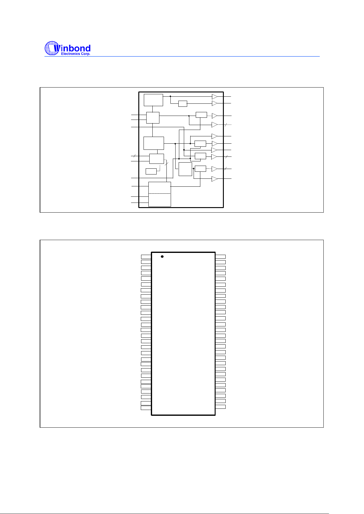
3.0 BLOCK DIAGRAM
PLL2
XTAL
OSC
Spread
Spectrum
PLL1
LATCH
POR
STOP
1/2
Control
Logic
Config.
Reg.
STOP
STOP
STOP
PCI
Clock
Divider
~
~
6
4
2
17
5
48MHz
24MHz
IOAPIC
REF(0:1)
CPUCLK_F
CPUCLK1
SDRAM(0:15)
PCICLK(0:4)
PCICLK_F
Xin
Xout
BUFFER IN
FS(0:3)*
4
MODE*
CPU_STOP#
PCI_STOP#
SDATA*
SDCLK*
SDRAM_F
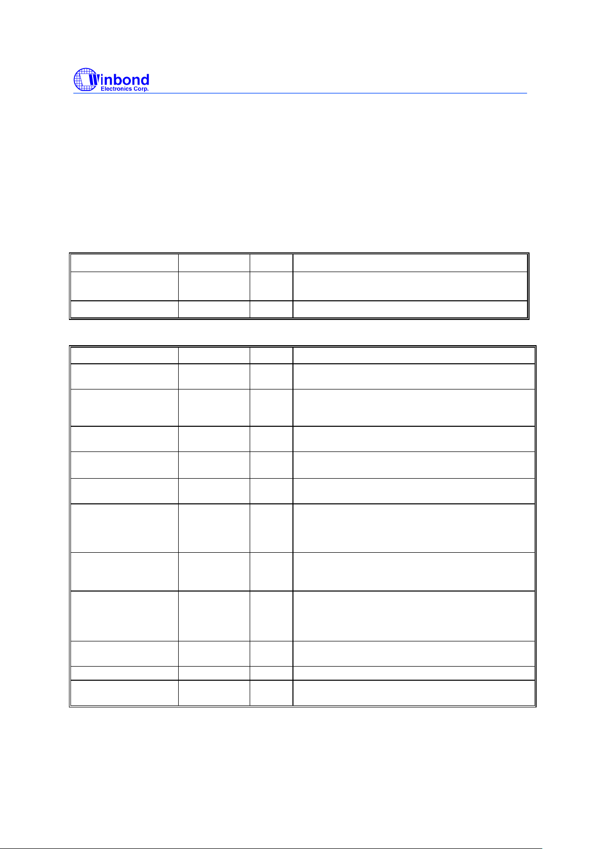
4.0 PIN CONFIGURATION
48
47
46
45
44
43
42
41
40
39
38
37
36
35
34
33
32
31
30
1
2
3
4
5
6
7
8
9
10
11
12
13
14
15
16
17
18
19
20
21
22
23
24
Vddq1
* PCI_STOP#/REF0
Vss
Xin
Xout
Vddq2
PCICLK_F/MODE*
PCICLK0/FS3*
Vss
PCICLK1
PCICLK2
PCICLK3
PCICLK4
Vddq2
BUFFER IN
SDRAM11
SDRAM10
Vddq3
SDRAM 9
SDRAM 8
Vss
SDATA
SDCLK
VddL1
IOAPIC0
IOAPIC_F
Vss
CPUCLK_F
CPUCLK1
VddL2
CPU_STOP#
SDRAM12
Vss
SDRAM 0
SDRAM 1
SDRAM 2
Vddq3
SDRAM 3
Vss
SDRAM 4
SDRAM 5
SDRAM 6
SDRAM 7
Vddq4
Vddq3
48MHz/FS0*
24MHz/FS1*
PCICLK5
29
26
27
28
25
55
54
53
52
51
50
49
56
SDRAM 15
SDRAM 14
Vss
REF1/ FS2*
SDRAM 12
SDRAM 13
Vss
SDRAM_F
W83195R-08
PRELIMINARY
Publication Release Date: Mar. 1999
- 3 - Revision 0.30
5.0 PIN DESCRIPTION
IN - Input
OUT - Output
I/O - Bi-directional Pin
# - Active Low
* - Internal 250kΩ pull-up
5.1 Crystal I/O
SYMBOL PIN I/O FUNCTION
Xin 5 IN Crystal input with internal loading capacitors and
feedback resistors.
Xout 6 OUT Crystal output at 14.318MHz nominally.
5.2 CPU, SDRAM, PCI, IOAPIC Clock Outputs
SYMBOL PIN I/O FUNCTION
CPUCLK_F 52 OUT Free running CPU clock. Not affected by
CPU_STOP#
CPUCLK1 51 OUT Low skew (< 250ps) clock outputs for host
frequencies such as CPU, Chipset and Cache.
Powered by VddL2. Low if CPU_STOP# is low.
CPU_STOP# 47 IN This asynchronous input halts CPUCLK1,IOAPIC &
SDRAM(0:12) at logic
“0”
level when driven low.
IOAPIC0 55 OUT High drive buffered output of the crystal, and is
powered by VddL1.
IOAPIC_F 54 OUT Free running IOAPIC clock, and not affected by
CPU_STOP#
SDRAM [ 0:15] 18,19,21,22,24
,25,32,33,35,
36,38,39,40,41
,43,44
OUT SDRAM clock outputs. Fanout buffer outputs from
BUFFER IN pin.(Controlled by chipset)
PCICLK_F/
*MODE
8 I/O Free running PCI clock during normal operation.
Latched Input. Mode=1, Pin 2 is REF0; Mode=0,
Pin2 is PCI_STOP#
PCICLK0/*FS3 9 I/O Low skew (< 250ps) PCI clock outputs.
Latched input for FS3 at initial power up for H/W
selecting the output frequency of CPU, SDRAM and
PCI clocks.
PCICLK [ 1:5 ] 11,12,13,14,16 OUT Low skew (< 250ps) PCI clock outputs. Synchronous
to CPU clocks with 1-48ns skew(CPU early).
BUFFER IN 17 IN Inputs to fanout for SDRAM outputs.
SDRAM_F 46 O Free running SDRAM clock, and not affected by
CPU_STOP#
W83195R-08
PRELIMINARY
Publication Release Date: Mar. 1999
- 4 - Revision 0.30
5.3 I2C Control Interface
SYMBOL PIN I/O FUNCTION
*SDATA 27 I/O Serial data of I2C 2-wire control interface with internal
pull-up resistor.
*SDCLK 28 IN Serial clock of I2C 2-wire control interface with
internal pull-up resistor.
5.4 Fixed Frequency Outputs
SYMBOL PIN I/O FUNCTION
REF0 / PCI_STOP# 3 I/O 14.318MHz reference clock. This REF output is the
stronger buffer for ISA bus loads.
Halt PCICLK(0:4) clocks at logic 0 level, when input
low (In mobile mode. MODE=0)
REF1 / *FS2 2 I/O 14.318MHz reference clock.
Latched input for FS2 at initial power up for H/W
selecting the output frequency of CPU, SDRAM and
PCI clocks.
24MHz / *FS0 30 I/O 24MHz output clock.
Latched input for FS1 at initial power up for H/W
selecting the output frequency of CPU, SDRAM and
PCI clocks.
48MHz / *FS1 29 I/O 48MHz output for USB during normal operation.
Latched input for FS0 at initial power up for H/W
selecting the output frequency of CPU, SDRAM and
PCI clocks.
5.5 Power Pins
SYMBOL PIN FUNCTION
Vddq1 1 Power supply for Ref [0:1] crystal and core logic.
VddL1 56 Power supply for IOAPIC output, either 2.5V or 3.3V.
VddL2 50 Power supply for CPUCLK_F & CPUCLK[1:2], either
2.5V or 3.3V.
Vddq2 7,15 Power supply for PCICLK_F, PCICLK[0:5], 3.3V.
Vddq3 20,37,45 Power supply for SDRAM_F & SDRAM[0:15], and CPU
PLL core, nominal 3.3V.
Vddq4 31 Power for 24 & 48MHz output buffers and fixed PLL
core.
Vss 4,10,23,26,34,42,48,53Circuit Ground.
W83195R-08
PRELIMINARY
Publication Release Date: Mar. 1999
- 5 - Revision 0.30
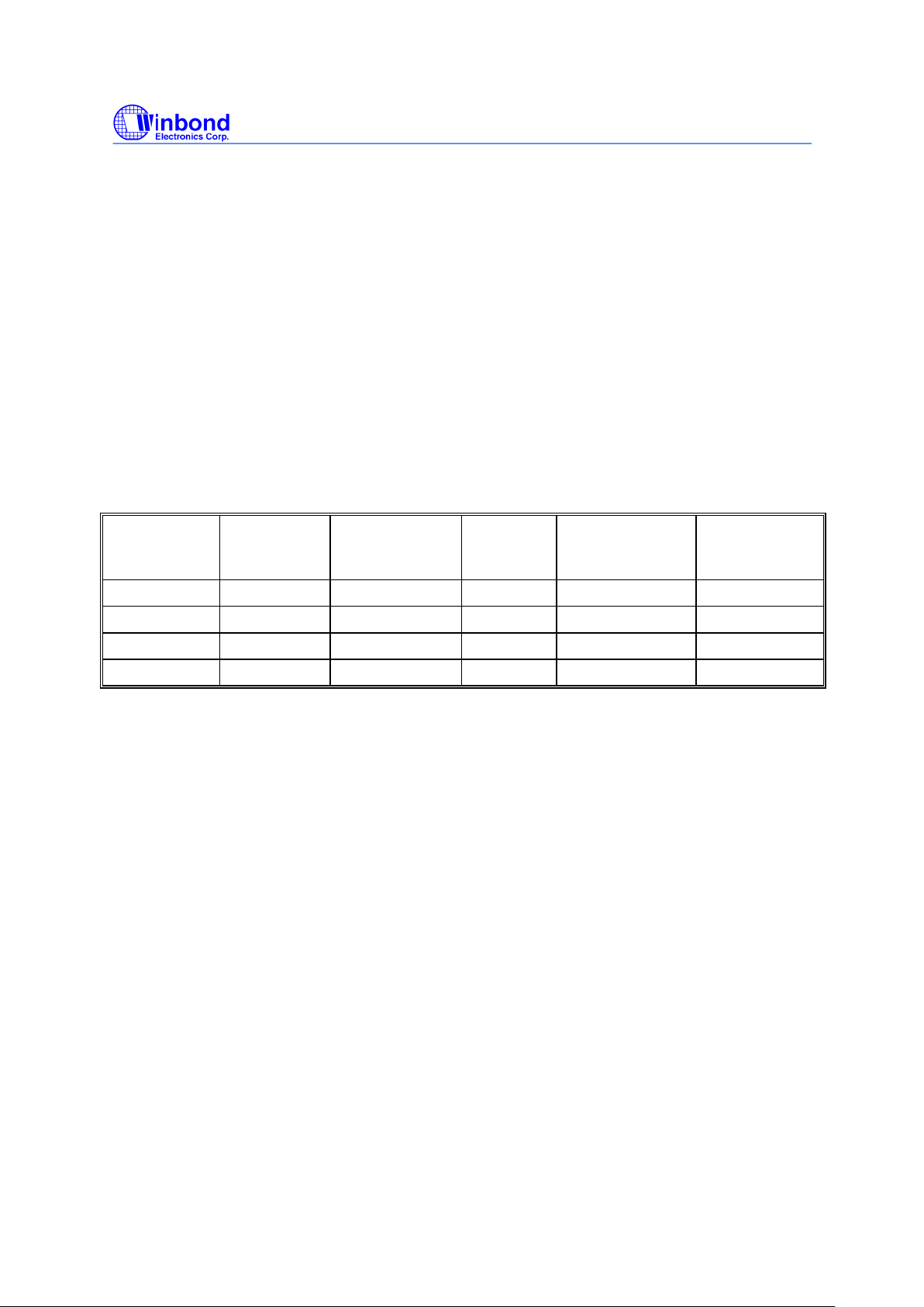
6.0 FREQUENCY SELECTION
FS3=0 CPU,SDRAM (MHz) PCI (MHz) REF,IOAPIC
FS2 FS1 FS0 (MHz)
0 0 0 124 41.33(CPU/3) 14.318
0 0 1 75 37.5(CPU/2) 14.318
0 1 0 83.3 41.65(CPU/2) 14.318
0 1 1 66.8 33.4(CPU/2) 14.318
1 0 0 103 34.3(CPU/3) 14.318
1 0 1 112 37.33(CPU/3) 14.318
1 1 0 133 44.33(CPU/3) 14.318
1 1 1 100.3 33.3(CPU/3) 14.318
FS3=1 CPU,SDRAM (MHz) PCI (MHz) REF,IOAPIC
FS2 FS1 FS0 (MHz)
0 0 0 120 40.00(CPU/3) 14.318
0 0 1 115 38.33(CPU/3) 14.318
0 1 0 110 36.67(CPU/3) 14.318
0 1 1 105 35.00(CPU/3) 14.318
1 0 0 140 35.00(CPU/4) 14.318
1 0 1 150 37.50(CPU/4) 14.318
1 1 0 124 31.00(CPU/4) 14.318
1 1 1 133 33.25(CPU/4) 14.318
7.0 MODE PIN -POWER MANAGEMENT INPUT CONTROL
MODE, Pin8 (Latched Input) PIN 3
0 PCI_STOP# (Input)
1 REF0 (Output)
W83195R-08
PRELIMINARY
Publication Release Date: Mar. 1999
- 6 - Revision 0.30
8.0 FUNTION DESCRIPTION
8.1 POWER MANAGEMENT FUNCTIONS
All clocks can be individually enabled or disabled via the 2-wire control interface. On power up,
external circuitry should allow 3 ms for the VCO’s to stabilize prior to enabling clock outputs to
assure correct pulse widths. When MODE=0, pins 3 and 47 are inputs (PCI_STOP#), (CPU_STOP#),
when MODE=1, these functions are not available. A particular clock can be enabled as both the 2wire serial control interface and one of these pins indicate that it should be enable.
The W83195R-08 may be disabled in the low state according to the following table in order to reduce
power consumption. All clocks are stopped in the low state, but maintain a valid high period on
transitions from running to stop. The CPU and PCI clocks transform between running and stop by
waiting for one positive edge on PCICLK_F followed by negative edge on the clock of interest, after
which high levels of the output are either enabled or disabled.
CPU_STOP# PCI_STOP# CPUCLK[1:2]
IOAPIC0 &
SDRAM [0:15]
PCI OTHER CLKs XTAL & VCOs
0 0 LOW LOW RUNNING RUNNING
0 1 LOW RUNNING RUNNING RUNNING
1 0 RUNNING LOW RUNNING RUNNING
1 1 RUNNING RUNNING RUNNING RUNNING
8.2 2-WIRE I2C CONTROL INTERFACE
The clock generator is a slave I2C component which can be read back the data stored in the latches
for verification. All proceeding bytes must be sent to change one of the control bytes. The 2-wire
control interface allows each clock output individually enabled or disabled. On power up, the
W83195R-08 initializes with default register settings. Use of the 2-wire control interface is then
optional.
The SDATA signal only changes when the SDCLK signal is low, and is stable when SDCLK is high
during normal data transfer. There are only two exceptions. One is a high-to-low transition on
SDATA while SDCLK is high used to indicate the beginning of a data transfer cycle. The other is a
low-to-high transition on SDATA while SDCLK is high used to indicate the end of a data transfer
cycle. Data is always sent as complete 8-bit bytes followed by an acknowledge generated.
Byte writing starts with a start condition followed by 7-bit slave address and a write command bit
[1101 0010], command code checking [0000 0000], and byte count checking. After successful
reception of each byte, an acknowledge (low) on the SDATA wire will be generated by the clock chip.
Controller can start to write to internal I2C registers after the string of data. The sequence order is as
follows:
 Loading...