

Winbond Electronics W83195BR-25 Datasheet

W83195BR-25
200MHZ 3-DIMM CLOCK FOR SOLANO CHIPSET
1.0 GENERAL DESCRIPTION
The W83195BR-25 is a Clock Synthesizer for Intel 815 Solano chipset. W83195BR-25 provides all
clocks required for high-speed RISC or CISC microprocessor and also provides 64 different
frequencies of CPU, SDRAM, PCI, 3V66, IOAPIC clocks frequency setting. All clocks are externally
selectable with smooth transitions.
The W83195BR-25 provides I2C serial bus interface to program the registers to enable or disable
each clock outputs and provides 0.25% and 0.5% center type spread spectrum to reduce EMI.
The W83195BR-25 provides stepless frequency programming by controlling the VCO freq. and the
clock output divisor ratio. Also skew of CPU,SDRAM and 3V66 clock outputs are programmable. A
watch dog timer is quipped and when time out, the RESET# pin will output 4ms pulse signal.
The W83195BR-25 accepts a 14.318 MHz reference crystal as its input and runs on a 3.3V supply.
High drive PCI and SDRAM CLOCK outputs typically provide greater than 1 V /ns slew rate into 30
pF loads. CPU CLOCK outputs typically provide better than 1 V /ns slew rate into 20 pF loads as
maintaining 50± 5% duty cycle. The fixed frequency outputs as REF, 24MHz, and 48 MHz provide
better than 0.5V /ns slew rate.
2.0 PRODUCT FEATURES
• 2 CPU clocks (2.5V)
• 3 3V-66 clocks (3.3V)
• 12 SDRAM clocks for 3 DIMMs(3.3V)
• 8 PCI synchronous clocks.
• Optional single or mixed supply:
(VDDR = VDDP=VDDS = VDD48 = VDD3 = 3.3V, VDDA=VDDC=2.5V)
• Skew form CPU to PCI clock -1 to 4 ns, center 2.6 ns
• Smooth frequency switch with selections from 66.8 to 200MHz
• I2C 2-Wire serial interface and I2C read back
• 0.25% center and 0.5% center type spread spectrum
• Programmable registers to enable/stop each output and select modes
(mode as Tri-state or Normal )
• 48 MHz for USB
• 24 MHz for super I/O
• Packaged in 56-pin SSOP
Publication Release Date: May 2000
- 1 - Revision 0.52
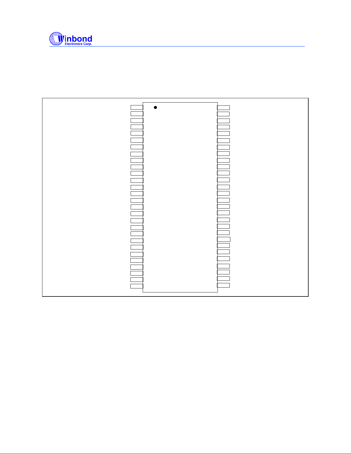
3.0 PIN CONFIGURATION
W83195BR-25
PRELIMINARY
VDDR
Xin
Xout
VSS
VSS
3V66-0
3V66-1
3V66-2
VDD3
VDDP
PCICLK0/ FS0&
PCICLK1/ *FS1
PCICLK2/SEL24_48*
VSS
PCICLK3^/Mode1*
PCICLK4^
PCICLK5^
VDDP
PCICLK6^
PCICLK7
VSS
PD#/RESET$
*SDCLK
*SDATA
VDDS
SDRAM 11
SDRAM 10
VSS
Note: * Internal pull-up
&: Internal pull-down
^ 1.5~2 strength
$: Open drain
1
2
3
4
5
6
7
8
9
10
11
12
13
14
15
16
17
18
19
20
21
22
23
24
25
26
27
28
56
55
54
53
52
51
50
49
48
47
46
45
44
43
42
41
40
39
38
37
36
35
34
33
32
31
30
29
REF0/ FS4&^
VddA
IOAPIC
VDDC
CPUCLK0
CPUCLK1
VSS
VSS
SDRAM 0
SDRAM 1
SDRAM 2
VDDS
SDRAM 3
SDRAM 4
SDRAM 5
VSS
SDRAM 6
SDRAM 7
SDRAM_F
VDDS
VSS
24_48MHz/ FS2&
48MHz/ *FS3 ^
VDD48
VDDS
SDRAM 8
SDRAM 9
VSS
4.0 PIN DESCRIPTION
IN - Input
OUT - Output
I/O - Bi-directional Pin
Publication Release Date: May 2000
- 2 - Revision 0.52
# - Active Low
PCICLK1/ *FS1
PCICLK2/ *SEL24_48
Latched input for SEL24_48 at initial power up for the
put frequency of 24MHz(HIGH) and 48MHz(LOW)
PCICLK3/ Mode1*
Latched input for Mode* pin at initial power up for the
* - Internal 250kΩ pull-up
4.1 Crystal I/O
Xin 2 IN Crystal input with internal loading capacitors(36pF)
Xout 3 OUT Crystal output at 14.318MHz nominally with internal
4.2 CPU, SDRAM, PCI, IOAPIC Clock Outputs
CPUCLK [0:1] 52,51 OUT Low skew (< 250ps) clock outputs for host
PD#/RESET$ 22 IN Mode1*=1, Power Down mode when driven low.
IOAPIC
SDRAM_F,
SDRAM[0:11]
PCICLK0/ FS0& 11 I/O 3.3V 33MHz PCI clock during normal operation.
W83195BR-25
PRELIMINARY
SYMBOL PIN I/O FUNCTION
and feedback resistors.
loading capacitors(36pF).
SYMBOL PIN I/O FUNCTION
frequencies such as CPU and Chipset.
Mode1*=0, RESET# open drain (4ms low active
pulse when Watch Dog time out)
54 OUT Clock outputs synchronous with PCI clock and
powered by VddA.
38, 48,47,46,
44,43,42,40,
39,31, 30,27,
26
12 I/O Low skew (< 250ps) PCI clock outputs.
13 I/O Low skew (< 250ps) PCI clock outputs.
OUT SDRAM clock outputs.
Latched input for FS0 at initial power up for H/W
selecting the output frequency of CPU, SDRAM and
PCI clocks(Default=0).
Latched input for FS1 at initial power up for H/W
selecting the output frequency of CPU, SDRAM and
PCI clocks(Default=1).
PCICLK [ 4:7 ] 16,17,19,20 OUT Low skew (< 250ps) PCI clock outputs.
3V66 [0:2] 6,7,8 OUT 3.3V output clocks for the chipset.
15 I/O Low skew (< 250ps) PCI clock outputs.
out
clocks.
output PD# /RESET# output selection.
Publication Release Date: May 2000
- 3 - Revision 0.52
W83195BR-25
wire control interface with internal
PRELIMINARY
4.3 I2C Control Interface
SYMBOL PIN I/O FUNCTION
*SDATA 24 I/O Serial data of I2C 2-
*SDCLK 23 IN Serial clock of I2C 2-wire control interface with
4.4 Fixed Frequency Outputs
SYMBOL PIN I/O FUNCTION
REF0 / FS4& 56 I/O 14.318MHz reference clock. This REF output is the
24_48MHz/FS2& 35 I/O 24MHz or 48MHz output clock. Default is 24MHz.
48MHz/ FS3* 34 I/O 48MHz / Latched input for FS3 at initial power up
pull-up resistor.
internal pull-up resistor.
stronger buffer for ISA bus loads.
Latched input for FS4 at initial power up for H/W
selecting the output frequency of CPU, SDRAM and
PCI clocks (Default=0).
Latched input for FS2 at initial power up for H/W
selecting the output frequency of CPU, SDRAM and
PCI clocks(Default=0).
for H/W selecting the output frequency of CPU,
SDRAM and PCI clocks (Default=1).
4.5 Power Pins
SYMBOL PIN FUNCTION
VddC,VddA 53,55 Power supply for CPU & IOAPIC, 2.5V or 3.3V.
Vdd48 33 Power supply for 48MHz output,3.3V.
Vdd3 9 Power supply for 3V_66 output, 3.3V.
VddP 10,18 Power supply for PCICLK, 3.3V.
VddR 1 Power supply for REF0, 3.3V.
VddS 45,37,32,25 Power supply for SDRAM_F,SDRAM[0:11], nominal
3.3V.
Vss 4,5,14,21,28,29,36,
41, 49.50
Circuit Ground.
Publication Release Date: May 2000
- 4 - Revision 0.52
W83195BR-25
PRELIMINARY
5.0 Frequency Selection BY hardware
FS4 FS3 FS2 FS1 FS0
0 0 0 0 0 55.00 82.50 55.00 27.50 13.75
0 0 0 0 1 60.00 90.00 60.00 30.00 15.00
0 0 0 1 0 66.80 100.20 66.80 33.40 16.70
0 0 0 1 1 68.33 102.50 68.33 34.17 17.08
0 0 1 0 0 70.00 105.00 70.00 35.00 17.50
0 0 1 0 1 72.00 108.00 72.00 36.00 18.00
0 0 1 1 0 75.00 112.50 75.00 37.50 18.75
0 0 1 1 1 77.00 115.50 77.00 38.50 19.25
0 1 0 0 0 83.30 83.30 55.53 27.77 13.88
0 1 0 0 1 90.00 90.00 60.00 30.00 15.00
0 1 0 1 0 100.30 100.30 66.87 33.43 16.72
0 1 0 1 1 103.00 103.00 68.67 34.33 17.17
0 1 1 0 0 112.50 112.50 75.00 37.50 18.75
0 1 1 0 1 115.00 115.00 76.67 38.33 19.17
0 1 1 1 0 120.00 120.00 80.00 40.00 20.00
0 1 1 1 1 125.00 125.00 83.33 41.67 20.83
1 0 0 0 0 128.00 128.00 64.00 32.00 16.00
1 0 0 0 1 130.00 130.00 65.00 32.50 16.25
1 0 0 1 0 133.70 133.70 66.85 33.43 16.71
1 0 0 1 1 137.00 137.00 68.50 34.25 17.13
1 0 1 0 0 140.00 140.00 70.00 35.00 17.50
1 0 1 0 1 145.00 145.00 72.50 36.25 18.13
1 0 1 1 0 150.00 150.00 75.00 37.50 18.75
1 0 1 1 1 153.33 153.33 76.67 38.33 19.17
1 1 0 0 0 125.00 93.75 62.50 31.25 15.63
1 1 0 0 1 130.00 97.50 65.00 32.50 16.25
1 1 0 1 0 133.70 100.28 66.85 33.43 16.71
1 1 0 1 1 137.00 102.75 68.50 34.25 17.13
1 1 1 0 0 140.00 105.00 70.00 35.00 17.50
1 1 1 0 1 145.00 108.75 72.50 36.25 18.13
1 1 1 1 0 150.00 112.50 75.00 37.50 18.75
1 1 1 1 1 153.33 115.00 76.67 38.33 19.17
CPU(MHz) SDRAM(MHz) 3V66(MHz) PCI(MHz) IOAPIC
(MHz)
Publication Release Date: May 2000
- 5 - Revision 0.52
W83195BR-25
PRELIMINARY
6. SERIAL CONTROL REGISTERS
The Pin column lists the affected pin number and the @PowerUp column gives the state at true
power up. Registers are set to the values shown only on true power up. "Command Code" byte and
"Byte Count" byte must be sent following the acknowledge of the Address Byte. Although the data
(bits) in these two bytes are considered "don't care", they must be sent and will be acknowledge.
After that, the below described sequence (Register 0, Register 1, Register 2, ....) will be valid and
acknowledged.
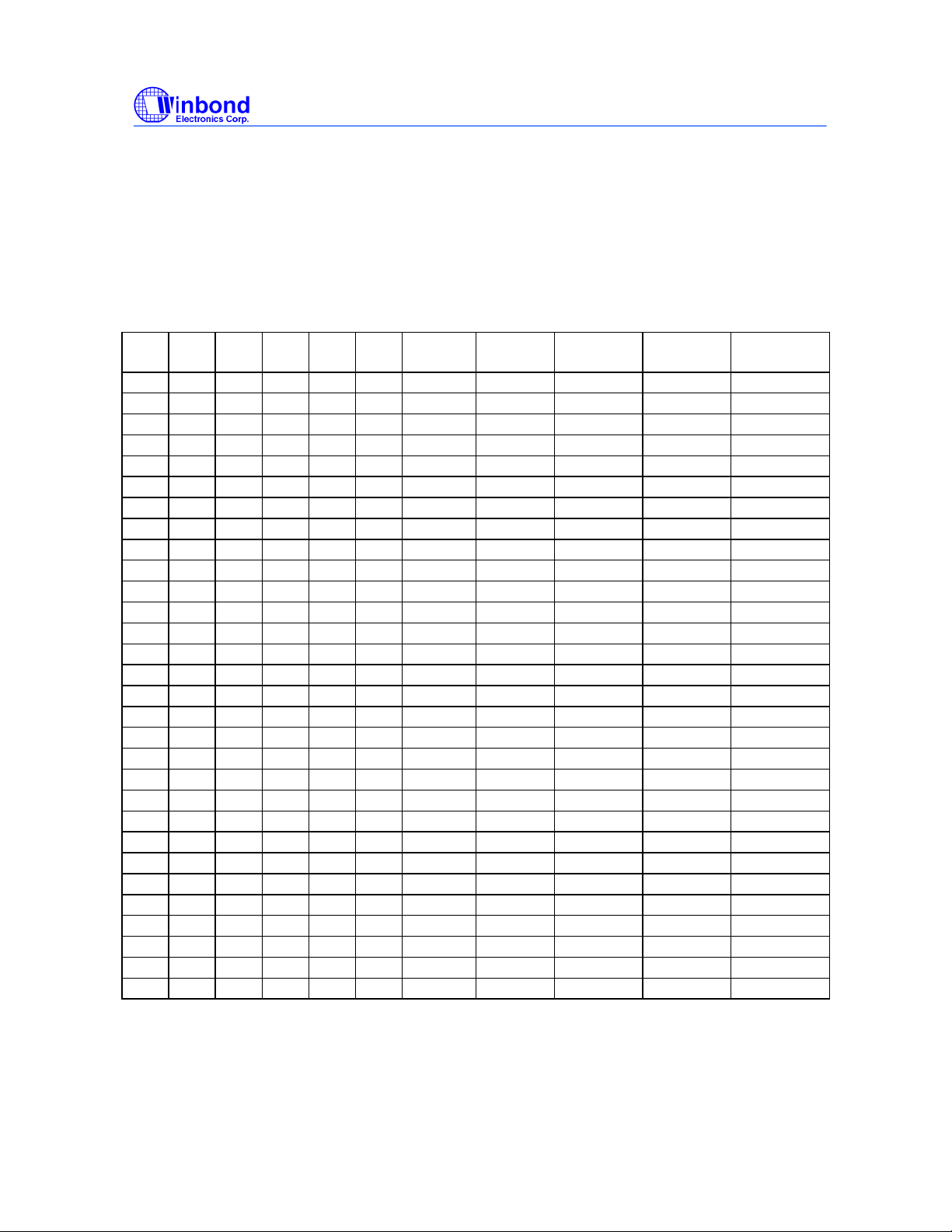
Frequency Table Setting by I2C (SEL5 ~ SEL0)
SSEL5 SSEL4 SSEL3 SSEL2 SSEL1 SSEL0
0 0 0 0 0 0 55.00
0 0 0 0 0 1 60.00
0 0 0 0 1 0 66.80 100.20
0 0 0 0 1 1 68.33 102.50
0 0 0 1 0 0 70.00 105.00
0 0 0 1 0 1 72.00 108.00
0 0 0 1 1 0 75.00 112.50
0 0 0 1 1 1 77.00 115.50
0 0 1 0 0 0 83.30
0 0 1 0 0 1 90.00
0 0 1 0 1 0 100.30 100.30
0 0 1 0 1 1 103.00 103.00
0 0 1 1 0 0 112.50 112.50
0 0 1 1 0 1 115.00 115.00
0 0 1 1 1 0 120.00 120.00
0 0 1 1 1 1 125.00 125.00
0 1 0 0 0 0 128.00 128.00
0 1 0 0 0 1 130.00 130.00
0 1 0 0 1 0 133.70 133.70
0 1 0 0 1 1 137.00 137.00
0 1 0 1 0 0 140.00 140.00
0 1 0 1 0 1 145.00 145.00
0 1 0 1 1 0 150.00 150.00
0 1 0 1 1 1 153.33 153.33
0 1 1 0 0 0 125.00 93.75 62.50 31.25 15.63
0 1 1 0 0 1 130.00 97.50 65.00 32.50 16.25
0 1 1 0 1 0 133.70 100.28
0 1 1 0 1 1 137.00 102.75
0 1 1 1 0 0 140.00 105.00
0 1 1 1 0 1 145.00 108.75
CPU
(MHz)
SDRAM
(MHz)
82.50 55.00 27.50 13.75
90.00 60.00 30.00 15.00
83.30 55.53 27.77 13.88
90.00 60.00 30.00 15.00
3V66
(MHz)
66.80 33.40 16.70
68.33 34.17 17.08
70.00 35.00 17.50
72.00 36.00 18.00
75.00 37.50 18.75
77.00 38.50 19.25
66.87 33.43 16.72
68.67 34.33 17.17
75.00 37.50 18.75
76.67 38.33 19.17
80.00 40.00 20.00
83.33 41.67 20.83
64.00 32.00 16.00
65.00 32.50 16.25
66.85 33.43 16.71
68.50 34.25 17.13
70.00 35.00 17.50
72.50 36.25 18.13
75.00 37.50 18.75
76.67 38.33 19.17
66.85 33.43 16.71
68.50 34.25 17.13
70.00 35.00 17.50
72.50 36.25 18.13
PCI(MHz)
IOAPIC
(MHz)
Publication Release Date: May 2000
- 6 - Revision 0.52
 Loading...