

Winbond Electronics W83194R-KX Datasheet

W83194R-KX
133MHZ 3-DIMM K7 CLOCK
1.0 GENERAL DESCRIPTION
The W83194R-KX is a clock generator which provides all clocks required for AMD K7 system.
W83194R-KX provides one differential pair CPU clock open drain outputs up to 143MHz which are
externally selectable with smooth transitions. W83194R-KX also provides 6 PCI clocks and 13
SDRAM clocks controlled by the none-delay buffer_in pin.
The W83194R-KX accepts a 14.318 MHz reference crystal as its input and runs on a 3.3V supply.
Spread spectrum built in at ±0.5% or ±0.25% to reduce EMI. Programmable stopping individual clock
outputs and frequency selection through I2C interface. The device meets the Pentium power-up
stabilization, which requires CPU and PCI clocks be stable within 2 ms after power-up.
High drive six PCI and thirteen SDRAM CLOCK outputs typically provide greater than 1 V /ns slew
rate into 30 pF loads. Two CPU CLOCK outputs typically provide better than 1 V /ns slew rate into 20
pF loads, when maintaining 50± 5% duty cycle. The fixed frequency outputs, such as REF, 24MHz,
and 48 MHz provide better than 0.5V /ns slew rate.
2.0 PRODUCT FEATURES
•
Supports AMD K7 CPU with I2C.
•
One pair of differential CPU clocks
•
One chipset clock
• 13 SDRAM clocks for 3 DIMMs
•
6 PCI synchronous clocks
•
Optional single or mixed supply:
(Vddq3=Vddq2 =3.3V) or (Vddq3 = 3.3V, Vddq2 = 2.5V)
•
< 250ps skew among CPU clocks
• < 250ps skew among PCI clocks
•
< 5ns propagation delay SDRAM from buffer input
•
Skew from CPU(earlier) to PCI clock 1.5 to 4ns, center 2.6ns.
•
Smooth frequency switch with selections from 66.8 MHz to 143 MHz CPU
•
I2C 2-Wire serial interface and I2C read back
•
± 0.25% or ± 0.5% spread spectrum function to reduce EMI
•
Programmable registers to enable/stop each output and select modes
(mode as Tri-state or Normal )
•
One 48 MHz for USB & one 24 MHz for super I/O
•
48-pin SSOP package
Publication Release Date: Nov. 1999
- 1 - Revision 0.35
~
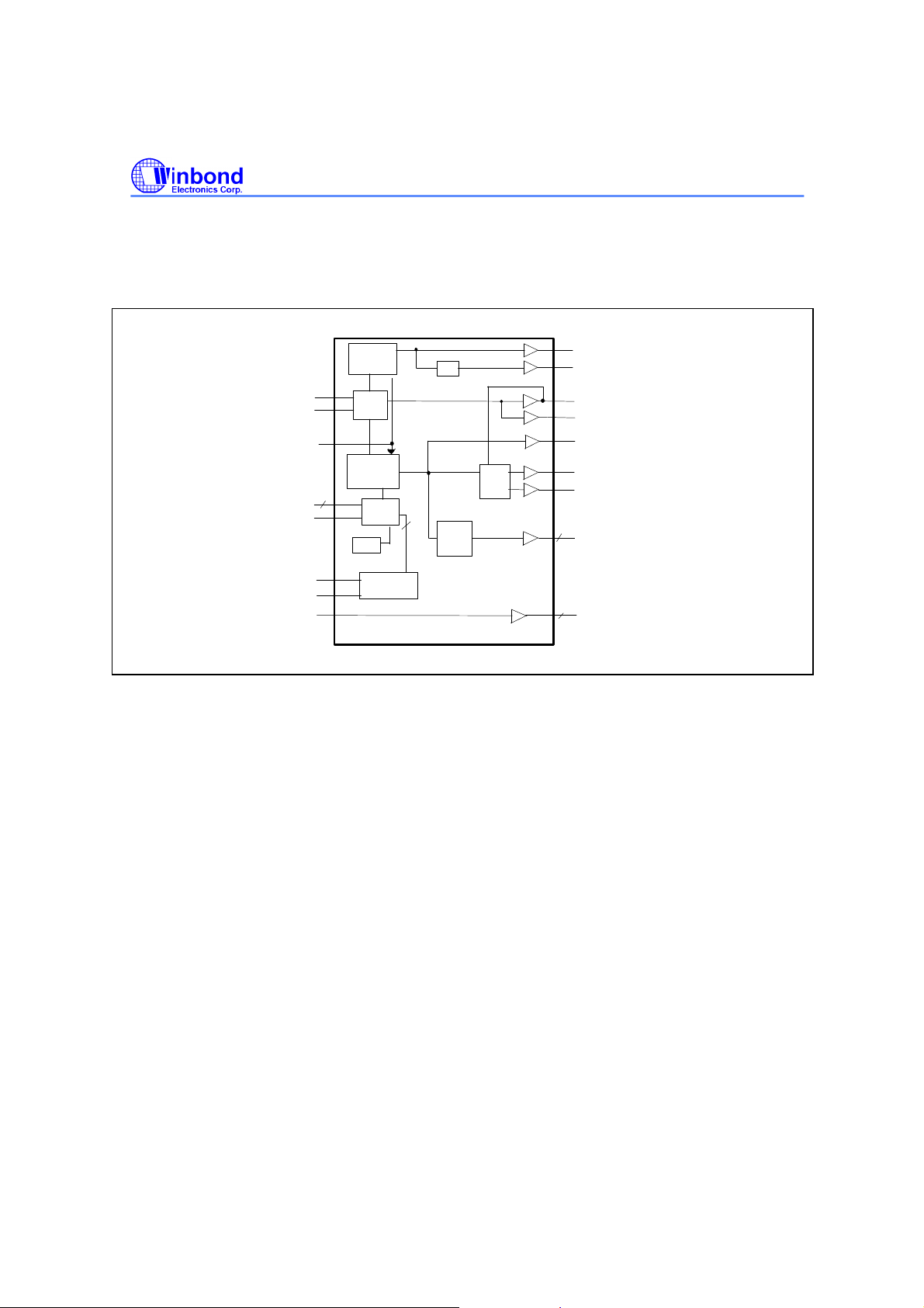
3.0 BLOCK DIAGRAM
W83194R-KX
PRELIMINARY
Xin
Xout
PD#
4
FS(0:3)*
MODE*
SDATA*
SDCLK*
BUFFER IN
4.0 PIN CONFIGURATION
PLL2
~
XTAL
OSC
PLL1
Spread
Spectrum
LATCH
POR
Config.
~
Reg.
48MHz
1/2
STOP
PCI
4
Clock
Divider
24_48MHz
REF0/CPU_STOP#
REF1
CPUT_CS
CPUT0
CPUC0
PCICLK(0:5)
6
SDRAM(0:12)
13
Publication Release Date: Nov. 1999
- 2 - Revision 0.35
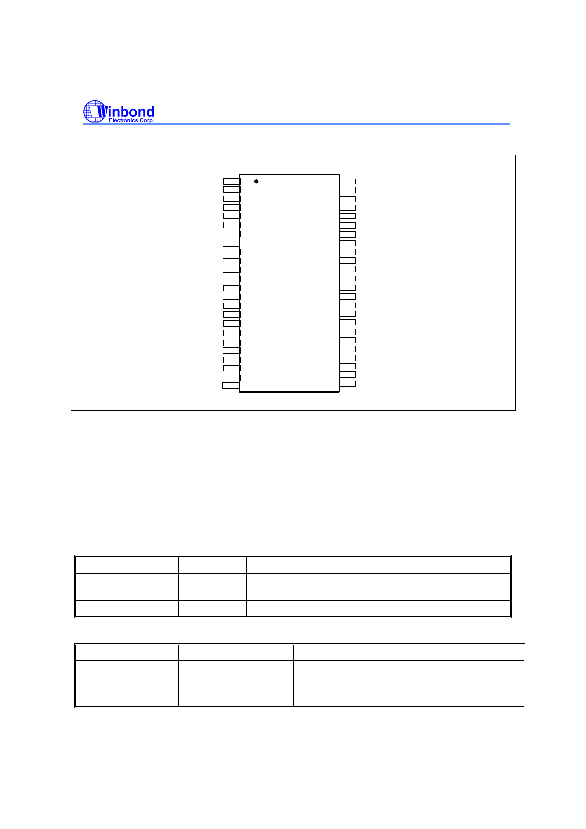
W83194R-KX
for the chipset. It has the same phase relationship as
PRELIMINARY
Vddq3
CPU_STOP#/REF0
Xout
Vddq3
PCICLK0/MODE*
PCICLK1/FS1*
PCICLK2
PCICLK3
PCICLK4
PCICLK5
Vddq3
BUFFER IN
SDRAM11
SDRAM10
Vddq3
SDRAM 9
SDRAM 8
SDATA*
SDCLK*
5.0 PIN DESCRIPTION
IN - Input
OUT - Output
I/O - Bi-directional Pin
# - Active Low
* - Internal 250kΩ pull-up
Vss
Xin
Vss
Vss
Vss
16
21
1
2
3
4
5
6
7
8
9
10
11
12
13
14
15
17
18
19
20
22
23
24
48
47
46
45
44
43
42
41
40
39
38
37
36
35
34
33
32
31
30
29
28
27
26
25
REF1/FS0*
Vss
CPUT_CS
Vss
CPUC0
CPUT0
VddQ2
PD#
SDRAM12
Vss
SDRAM 0
SDRAM 1
Vddq3
SDRAM 2
SDRAM 3
Vss
SDRAM 4
SDRAM 5
Vddq3
SDRAM 6
SDRAM 7
Vddq3
48MHz/FS2*
24_48MHz/FS3*
5.1 Crystal I/O
SYMBOL PIN I/O FUNCTION
Xin 4 IN Crystal input with internal loading capacitors and
Xout 5 OUT Crystal output at 14.318MHz nominally.
5.2 CPU, SDRAM, PCI, IOAPIC Clock Outputs
SYMBOL PIN I/O FUNCTION
CPUT_CS
CPU_C0
CPU_T0
46
44
43
feedback resistors.
OD CPU_C0 and CPU_T0 are the differential open drain
CPU clocks for K7. CPUT_CS is the open drain pin
CPU_T0.
Publication Release Date: Nov. 1999
- 3 - Revision 0.35
Low skew (< 250ps) PCI clock outputs. Synchronous
SDRAM [ 0:12] 17,18,20,21,28,2
9,31,32,34,
35,37,38,40
PCICLK0/
*MODE
PCICLK1/*FS1
PCICLK [ 2:5 ] 10,11,12,13 OUT
BUFFER IN 15 IN Inputs to fanout for SDRAM outputs.
PD# 41 IN The all clocks will be stopped when this pin set to
7 I/O Free running PCI clock during normal operation.
8 I/O Low skew (< 250ps) PCI clock outputs.
W83194R-KX
PRELIMINARY
OUT SDRAM clock outputs. Fanout buffer outputs from
BUFFER IN pin.(Controlled by chipset) They are
disabled when PD# is set LOW.
Latched Input. Mode=1, Pin 2 is REF0; Mode=0,
Pin2 is CPU_STOP#
Latched input for FS1 at initial power up for H/W
selecting the output frequency of CPU, SDRAM and
PCI clocks.
to CPU clocks with 1-48ns skew(CPU early).
LOW .
Publication Release Date: Nov. 1999
- 4 - Revision 0.35
 Loading...