

Winbond Electronics W83194R-81 Datasheet

W83194R-81
100MHZ CLOCK FOR SIS CHIPSET
1.0 GENERAL DESCRIPTION
The W83194R-81 is a Clock Synthesizer for SiS chipset. W83194R-81 provides all clocks required
for high-speed RISC or CISC microprocessor such as AMD,Cyrix,Intel Pentium and also provides 16
different frequencies of CPU clocks frequency setting. All clocks are externally selectable with
smooth transitions. The W83194R-81 makes SDRAM in synchronous or asynchronous frequency
with CPU clocks.
The W83194R-81 provides I2C serial bus interface to program the registers to enable or disable each
clock outputs and W83194R-81 provides the 0.25%, 0.5% center type spread spectrum to reduce
EMI.
The W83194R-81 accepts a 14.318 MHz reference crystal as its input and runs on a 3.3V supply.
High drive PCI and SDRAM CLOCK outputs typically provide greater than 1 V /ns slew rate into 30
pF loads. CPU CLOCK outputs typically provide better than 1 V /ns slew rate into 20 pF loads as
maintaining 50¡Ó 5% duty cycle. The fixed frequency outputs as REF, 24MHz, and 48 MHz provide
better than 0.5V /ns slew rate.
2.0 PRODUCT FEATURES
• Supports Pentium, Pentium Pro, AMD and Cyrix CPUs with I2C.
• 3 CPU clocks
• 13 SDRAM clocks for 3 DIMMs
• 6 PCI synchronous clocks.
• Optional single or mixed supply:
(Vdd = Vddq4=Vddq3 = Vddq2b = 3.3V, Vddq2=2.5V) or
(Vdd = Vddq4=Vddq3 = 3.3V, Vddq2=Vdq2b = 2.5V)
• Skew form CPU to PCI clock -1 to 4 ns, center 2.6 ns
• SDRAM frequency synchronous or asynchronous to CPU clocks
• Smooth frequency switch with selections from 66 to 133mhz(including 90MHz)
• I2C 2-Wire serial interface and I2C read back
• 0.25%, 0.5% center type spread spectrum to reduce EMI
• Programmable registers to enable/stop each output and select modes
(mode as Tri-state or Normal )
• MODE pin for power Management
• 48 MHz for USB
• 24 MHz for super I/O
• 48-pin SSOP package
Publication Release Date: Dec. 1998
- 1 - Revision 0.20
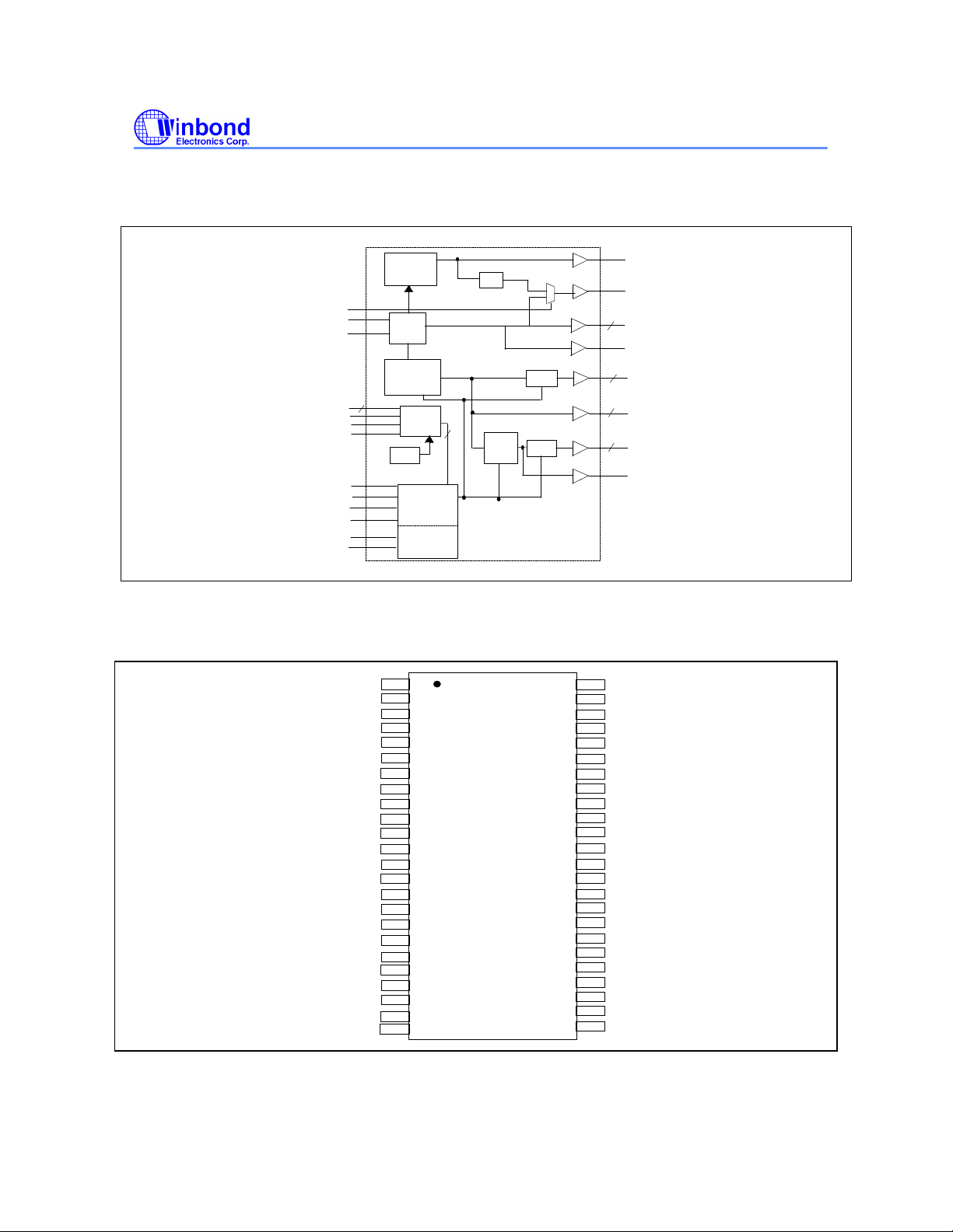
3.0 BLOCK DIAGRAM
W83194R-81
PRELIMINARY
SEL24_14#
*FS(0:2)
*MODE
CPU3.3_2.5#
*SD_SEL#
SDRAM_STOP#
CPU_STOP#
PCI_STOP#
*SDAT
*SCLK
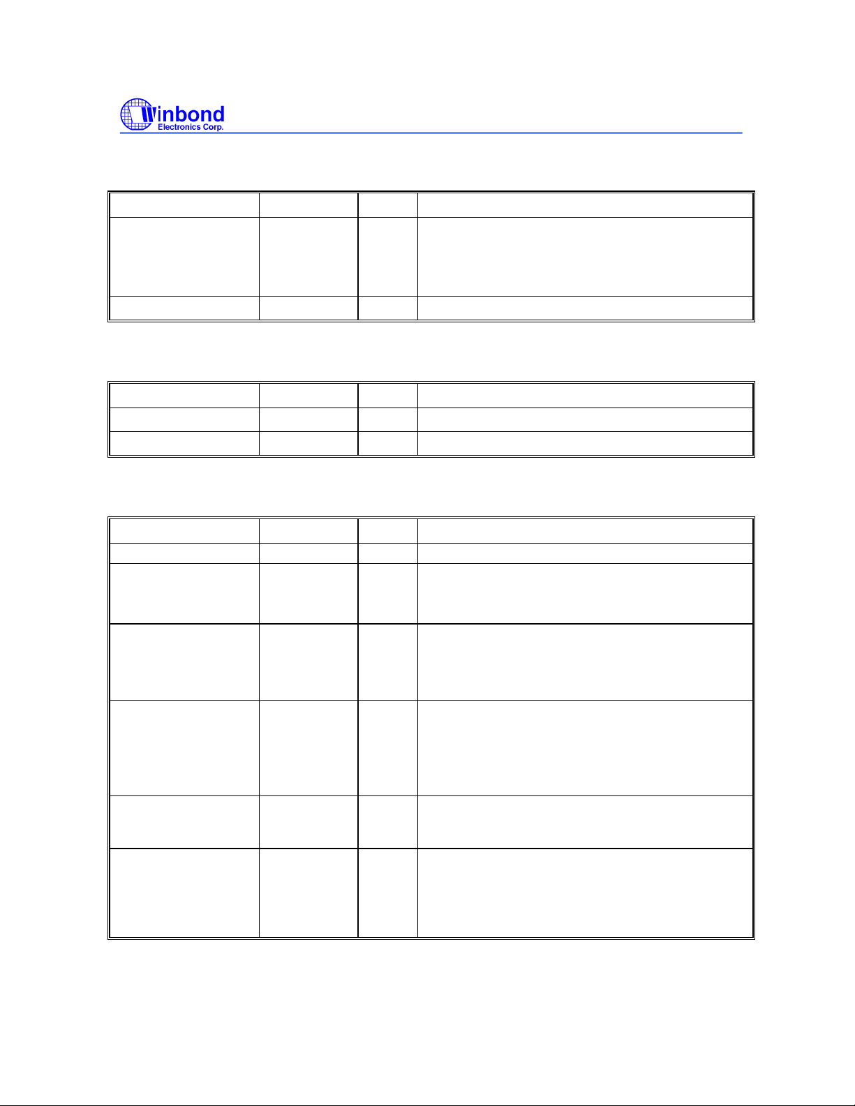
4.0 PIN CONFIGURATION
REF0/ *MODE
PCICLK_F/ *FS1
PCICLK0/ *FS2
PCICLK1
PCICLK2
PCICLK3
PCICLK4
SDRAM12
*CPU_STOP#/SDRAM11
*PCI_STOP#/SDRAM10
*SDRAM_STOP#/SDRAM 9
*PD#/SDRAM 8
Xin
Xout
PD#
Vdd
Vss
Xin
Xout
Vddq4
Vss
Vddq4
Vss
Vddq3
Vss
*SDATA
*SDCLK
PLL2
XTAL
OSC
PLL1
Spread
Spectrum
3
LATCH
POR
Contro
l Logic
5
¡Ò
2
CPU_STOP#
PCI
clock
Divder
PCI_STOP#
STOP
STOP
48MHz
SIO
REF(0:2)
3
IOAPIC
CPUCLK(0:2)
3
SDRAM(0:12)
13
PCICLK(0:4)
5
PCICLK_F
Config
. Reg.
Vddq2
IOAPIC
REF1/ *SD_SEL#
Vss
REF2/CPU3.3_2.5#
CPUCLK0
Vddq2b
CPUCLK1
CPUCLK
Vss
SDRAM 0
SDRAM 1
Vddq3
SDRAM 2
SDRAM 3
Vss
SDRAM 4
SDRAM 5
Vddq3
SDRAM 6
SDRAM 7
Vss
48MHz/*FS0
SIO/*SEL24_14#
16
21
1
2
3
4
5
6
7
8
9
10
11
12
13
14
15
17
18
19
20
22
23
24
48
47
46
45
44
43
42
41
40
39
38
37
36
35
34
33
32
31
30
29
28
27
26
25
Publication Release Date: Dec. 1998
- 2 - Revision 0.20

W83194R-81
PRELIMINARY
5.0 PIN DESCRIPTION
IN - Input
OUT - Output
I/O - Bi-directional Pin
# - Active Low
* - Internal 250kΩ pull-up
5.1 Crystal I/O
SYMBOL PIN I/O FUNCTION
Xin 4 IN Crystal input with internal loading capacitors and
feedback resistors.
Xout 5 OUT Crystal output at 14.318MHz nominally.
5.2 CPU, SDRAM, PCI Clock Outputs
SYMBOL PIN I/O FUNCTION
CPUCLK [ 0:2 ] 40,41,43 OUT Low skew (< 250ps) clock outputs for host
frequencies such as CPU, Chipset and Cache.
Vddq2b is the supply voltage for these outputs.
SDRAM11/
*CPU_STOP#
SDRAM10/
*PCI_STOP#
SDRAM9/
*SDRAM_STOP#
SDRAM8/ *PD# 21 I/O If MODE = 1 (default), then this pin is a SDRAM
SDRAM[0:7],
SDRAM12
PCICLK_F/ *FS1 7 I/O Latched input for FS1 at initial power up for H/W
17 I/O If MODE =1 (default), then this pin is a SDRAM clock
buffered output of the crystal. If MODE = 0 , then this
pin is CPU_STOP# input used in power
management mode for synchronously stopping the
all CPU clocks.
18 I/O If MODE = 1 (default), then this pin is a SDRAM
clock output. If MODE = 0 , then this pin is
PCI_STOP # and used in power management mode
for synchronously stopping the all PCI clocks.
20 I/O If MODE = 1 (default), then this pin is a SDRAM
clock output. If MODE = 0 , then this pin is
SDRAM_STOP # and used in power management
mode for stopping the all SDRAM clocks.
clock output. If MODE = 0 , then this pin is PD # and
used to power down the device into a power down
state.
28,29,31,32,34
, 35,37,38,15
O SDRAM clock outputs which have the same
frequency as CPU clocks.
selecting the output frequency of CPU, SDRAM and
PCI clocks.
Free running PCI clock during normal operation.
Publication Release Date: Dec. 1998
- 3 - Revision 0.20
W83194R-81
PRELIMINARY
5.2 CPU, SDRAM, PCI Clock Outputs, continued
SYMBOL PIN I/O FUNCTION
PCICLK 0 / *FS2 8 I/O Latched input for FS2 at initial power up for H/W
selecting the output frequency of CPU, SDRAM and
PCI clocks.
PCI clock during normal operation.
PCICLK [ 1:4 ] 10,11,12,13 OUT Low skew (< 250ps) PCI clock outputs.
5.3 I2C Control Interface
SYMBOL PIN I/O FUNCTION
*SDATA 23 I/O Serial data of I2C 2-wire control interface
*SDCLK 24 IN Serial clock of I2C 2-wire control interface
5.4 Fixed Frequency Outputs
SYMBOL PIN I/O FUNCTION
IOAPIC 47 O 2.5V fixed 14.318MHz
REF0 / *MODE 2 I/O 3.3V, 14.318MHz reference clock output.
Internal 250kΩ pull-up.
Function select pin.
REF1 /*SD_SEL# 46 I/O 3.3V, 14.318MHz reference clock output
Internal 250kΩ pull-up.
Latched input at Power On selects the frequencies
for clock outputs.
REF2 / CPU3.3#_2.5 44 I/O
SIO / *SEL24_14# 25 I/O *SEL24_14# controls the frequency of SIO. If logic 0
48MHz / *FS0 26 I/O
Internal 250kΩ pull-up.
Latched input for CPU3.3#_2.5 at initial power up.
Reference clock during normal operation.
Latched high - Vddq2b = 2.5V
Latched low - Vddq2b = 3.3V
at power on, SIO=14.318. If logic 1, SIO=24MHz for
super I/O.
Internal 250kΩ pull-up.
Latched input for FS0 at initial power up for H/W
selecting the output frequency of CPU, SDRAM and
PCI clocks. 48MHz output for USB during normal
operation.
Publication Release Date: Dec. 1998
- 4 - Revision 0.20
W83194R-81
PRELIMINARY
5.5 Power Pins
SYMBOL PIN FUNCTION
Vdd 1 Power supply for REF0 crystal and core logic.
Vddq2 48 Power supply for REF1,IOAPIC output, 2.5V.
Vddq2b 42 Power supply for REF2, CPUCLK[0:2], either 2.5V or
3.3V.
Vddq3 19, 30, 36 Power supply for SDRAM and 48/24MHz outputs.
Vddq4 6,14 Power supply for PCICLK outputs.
Vss 3,9,16,22,27,
33,39,45
Circuit Ground.
6.0 FREQUENCY SELECTION BY HARDWARE
SD_SEL FS2 FS1
0 0 0 0 66.70 100.05 33.35 14.318
0 0 0 1 90 90 30 14.318
0 0 1 0 95.25 63.4 31.7 14.318
0 0 1 1 100.2 66.8 33.4 14.318
0 1 0 0 100 75 30 14.318
0 1 0 1 112 74.7 37.3 14.318
0 1 1 0 124 82.7 31 14.318
0 1 1 1 133.3 88.9 33.3 14.318
1 0 0 0 66.8 66.8 33.4 14.318
1 0 0 1 75 75 30 14.318
FS0 CPU
(MHz)
SDRAM
(MHz)
PCI
(MHz)
REF (MHz)
IOAPIC
1 0 1 0 83.3 83.3 33.32 14.318
1 0 1 1 95.25 95.25 31.7 14.318
1 1 0 0 100.2 100.2 33.4 14.318
1 1 0 1 112 112 37.3 14.318
1 1 1 0 124 124 31 14.318
1 1 1 1 133.3 133.3 33.3 14.318
Publication Release Date: Dec. 1998
- 5 - Revision 0.20
7.0 CPU 3.3#_2.5 BUFFER SELECTION
CPU 3.3#_2.5 ( Pin 44 ) Input Level CPU Operate at
1 VDD = 2.5V
0 VDD = 3.3V
W83194R-81
PRELIMINARY
Publication Release Date: Dec. 1998
- 6 - Revision 0.20
 Loading...